Analog Devices ADG738 9 Datasheet

CMOS, Low-Voltage, 3-Wire
S1
S8
SCLKDDIN
SYNC
ADG738
S1A
SCLK
DA
DIN
S4A
S1B
S4B
DB
ADG739
RESET
DOUT
DOUT
SYNC
INPUT SHIFT
REGISTER
INPUT SHIFT
REGISTER
a
FEATURES
3-Wire Serial Interface
2.7 V to 5.5 V Single Supply
2.5 ⍀ On Resistance
0.75 ⍀ On-Resistance Flatness
100 pA Leakage Currents
Single 8-to-1 Multiplexer ADG738
Dual 4-to-1 Multiplexer ADG739
Power-On Reset
TTL/CMOS-Compatible
APPLICATIONS
Data Acquisition Systems
Communication Systems
Relay Replacement
Audio and Video Switching
Serially-Controlled, Matrix Switches
ADG738/ADG739
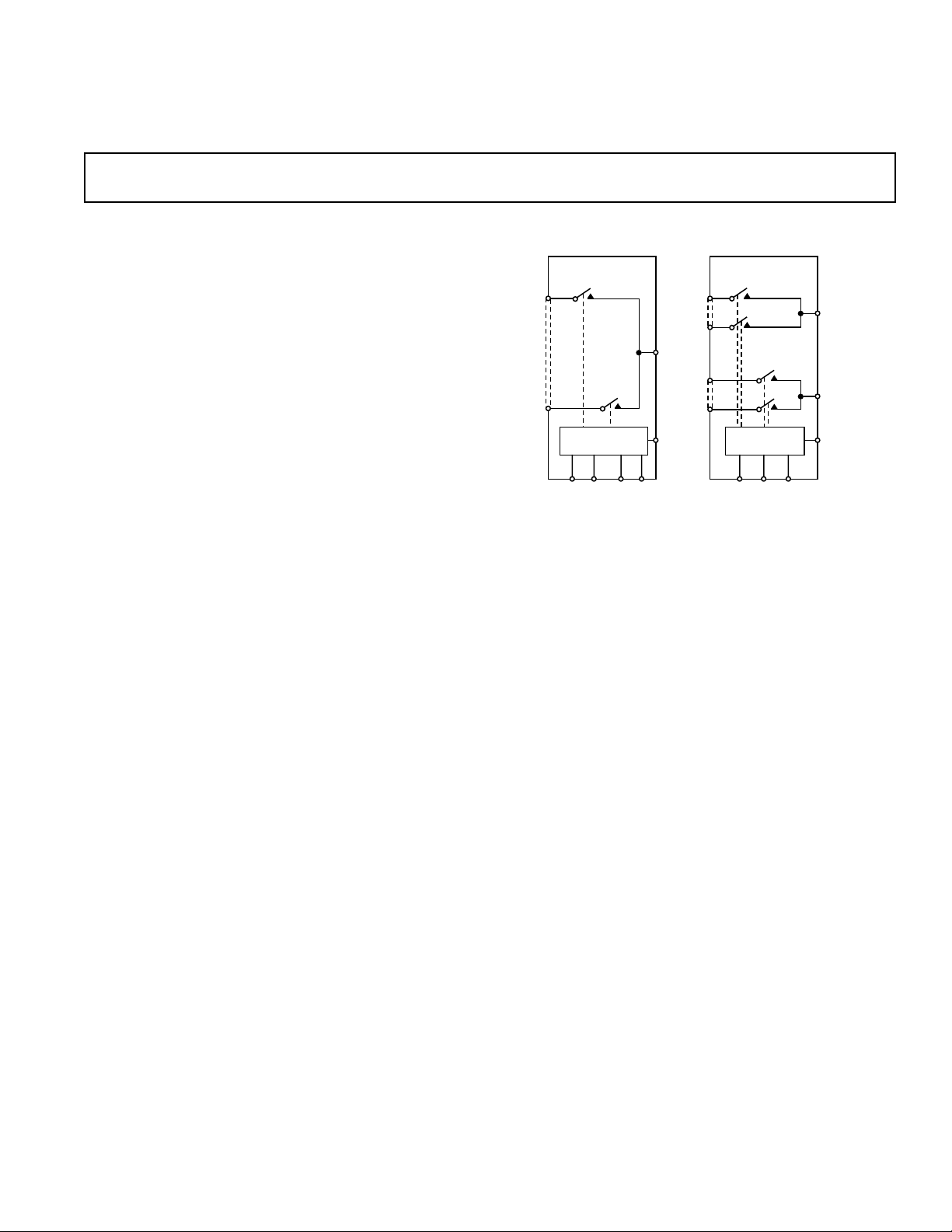
FUNCTIONAL BLOCK DIAGRAMS
GENERAL DESCRIPTION
The ADG738 and ADG739 are CMOS analog matrix switches
with a serially-controlled 3-wire interface. The ADG738 is an
8-channel matrix switch, while the ADG739 is a dual 4-channel
matrix switch. On resistance is closely matched between switches
and very flat over the full signal range.
The ADG738 and ADG739 utilize a 3-wire serial interface that
is compatible with SPI™, QSPI™, MICROWIRE™, and some
DSP interface standards. The output of the shift register DOUT
enables a number of these parts to be daisy-chained. On power-up,
PRODUCT HIGHLIGHTS
1. 3-Wire Serial Interface.
2. Single Supply Operation. The ADG738 and ADG739 are
fully specified and guaranteed with 3 V and 5 V supply rails.
3. Low On Resistance, 2.5 Ω typical.
4. Any configuration of switches may be on or off at any one time.
5. Guaranteed Break-Before-Make Switching Action.
6. Small 16-lead TSSOP Package.
the internal shift register contains all zeros and all switches
are in the OFF state.
Each switch conducts equally well in both directions when on,
making these parts suitable for both multiplexing and demultiplexing applications. As each switch is turned on or off by a
separate bit, these parts can also be configured as a type of switch
array, where any, all, or none of the eight switches may be closed
at any time. The input signal range extends to the supply rails.
All channels exhibit break-before-make switching action,
preventing momentary shorting when switching channels.
The ADG738 and ADG739 are available in 16-lead TSSOP
packages.
SPI and QSPI are trademarks of Motorola, Inc.
MICROWIRE is a trademark of National Semiconductor Corporation.
REV. 0
Information furnished by Analog Devices is believed to be accurate and
reliable. However, no responsibility is assumed by Analog Devices for its
use, nor for any infringements of patents or other rights of third parties
which may result from its use. No license is granted by implication or
otherwise under any patent or patent rights of Analog Devices.
One Technology Way, P.O. Box 9106, Norwood, MA 02062-9106, U.S.A.
Tel: 781/329-4700 World Wide Web Site: http://www.analog.com
Fax: 781/326-8703 © Analog Devices, Inc., 2000

1
ADG738/ADG739–SPECIFICATIONS
B Version
–40ⴗC
Parameter 25ⴗC to +85ⴗC Unit Test Conditions/Comments
ANALOG SWITCH
Analog Signal Range 0 V to V
On Resistance (R
On-Resistance Match Between 0.4 Ω typ V
Channels (∆R
On-Resistance Flatness (R
LEAKAGE CURRENTS V
Source OFF Leakage I
Drain OFF Leakage I
Channel ON Leakage I
DIGITAL INPUTS
Input High Voltage, V
Input Low Voltage, V
Input Current, I
CIN, Digital Input Capacitance 3 pF typ
DIGITAL OUTPUT
Output Low Voltage 0.4 max I
C
, Digital Output Capacitance 4 pF typ
OUT
DYNAMIC CHARACTERISTICS
t
ON
t
OFF
Break-Before-Make Time Delay, t
Charge Injection ± 3 pC typ V
Off Isolation –55 dB typ R
Channel-to-Channel Crosstalk –55 dB typ RL = 50 Ω, CL = 5 pF, f = 10 MHz;
–3 dB Bandwidth
ADG738 65 MHz typ RL = 50 Ω, CL = 5 pF, Test Circuit 8
ADG739 100 MHz typ
CS (OFF) 13 pF typ
CD (OFF)
ADG738 85 pF typ
ADG739 42 pF typ
CD, CS (ON)
ADG738 96 pF typ
ADG739 48 pF typ
POWER REQUIREMENTS V
I
DD
NOTES
1
Temperature range is as follows: B Version: –40°C to +85°C.
2
Guaranteed by design, not subject to production test.
Specifications subject to change without notice.
) 2.5 Ω typ VS = 0 V to VDD, IS = 10 mA;
ON
4.5 5 Ω max Test Circuit 1
) 0.8 Ω max
ON
FLAT(ON)
)0.75 Ω typ VS = 0 V to VDD, IS = 10 mA
1.2 Ω max
(OFF) ± 0.01 nA typ VD = 4.5 V/1 V, VS = 1 V/4.5 V;
S
± 0.1 ± 0.3 nA max Test Circuit 2
(OFF) ± 0.01 nA typ VD = 4.5 V/1 V, VS = 1 V/4.5 V;
D
± 0.1 ± 1 nA max Test Circuit 3
, IS (ON) ±0.01 nA typ VD = VS = 1 V/4.5 V, Test Circuit 4
D
± 0.1 ± 1 nA max
2.4 V min
0.8 V max
INL
INL
or I
INH
INH
0.005 µA typ VIN = V
± 0.1 µA max
2
20 ns typ RL = 300 Ω, CL = 35 pF, Test Circuit 5;
32 ns max V
10 ns typ RL = 300 Ω, CL = 35 pF, Test Circuit 5;
17 ns max V
D
9 ns typ RL = 300 Ω, CL = 35 pF;
1 ns min V
–75 dB typ RL = 50 Ω, CL = 5 pF, f = 1 MHz;
–75 dB typ RL = 50 Ω, CL = 5 pF, f = 1 MHz;
10 µA typ Digital Inputs = 0 V or 5.5 V
20 µA max
(VDD = 5 V ⴞ 10%, GND = 0 V, unless otherwise noted.)
V
DD
= 0 V to V
S
= 5.5 V
DD
or V
INL
= 6 mA
SINK
= 3 V
S1
= 3 V
S1
= VS8 = 3 V, Test Circuit 5
S1
= 2.5 V, RS = 0 Ω, CL = 1 nF;
S
DD, IS
INH
= 10 mA
Test Circuit 6
= 50 Ω, CL = 5 pF, f = 10 MHz;
L
Test Circuit 8
Test Circuit 7
= 5.5 V
DD
–2– REV. 0

ADG738/ADG739
1
SPECIFICATIONS
Parameter 25ⴗC to +85ⴗC Unit Test Conditions/Comments
ANALOG SWITCH
Analog Signal Range 0 V to V
On Resistance (R
On-Resistance Match Between 0.4 Ω typ V
Channels (∆R
On-Resistance Flatness (R
LEAKAGE CURRENTS V
Source OFF Leakage I
Drain OFF Leakage I
Channel ON Leakage I
DIGITAL INPUTS
Input High Voltage, V
Input Low Voltage, V
Input Current, I
CIN, Digital Input Capacitance 3 pF typ
DIGITAL OUTPUT
Output Low Voltage 0.4 max I
C
, Digital Output Capacitance 4 pF typ
OUT
DYNAMIC CHARACTERISTICS
t
ON
t
OFF
Break-Before-Make Time Delay, t
Charge Injection ± 3 pC typ V
Off Isolation –55 dB typ R
Channel-to-Channel Crosstalk –55 dB typ RL = 50 Ω, CL = 5 pF, f = 10 MHz;
–3 dB Bandwidth
ADG738 65 MHz typ RL = 50 Ω, CL = 5 pF, Test Circuit 8
ADG739 100 MHz typ
CS (OFF) 13 pF typ
CD (OFF)
ADG738 85 pF typ
ADG739 42 pF typ
CD, CS (ON)
ADG738 96 pF typ
ADG739 48 pF typ
POWER REQUIREMENTS V
I
DD
NOTES
1
Temperature ranges are as follows: B Versions: –40°C to +85°C.
2
Guaranteed by design, not subject to production test.
Specifications subject to change without notice.
)6 Ω typ VS = 0 V to VDD, IS = 10 mA;
ON
) 1.2 Ω max
ON
(OFF) ± 0.01 nA typ VS = 3 V/1 V, VD = 1 V/3 V;
S
(OFF) ± 0.01 nA typ VD = 3 V/1 V, VD = 1 V/3 V;
D
, IS (ON) ± 0.01 nA typ VD = VS = 3 V/1 V, Test Circuit 4
D
INH
INL
or I
INL
INH
(VDD = 3 V ⴞ 10%, GND = 0 V, unless otherwise noted.)
B Version
–40ⴗC
DD
11 12 Ω max Test Circuit 1
FLAT(ON)
) 3.5 Ω typ VS = 0 V to VDD, IS = 10 mA
± 0.1 ± 0.3 nA max Test Circuit 2
± 0.1 ± 1 nA max Test Circuit 3
± 0.1 ± 1 nA max
2.0 V min
0.4 V max
0.005 µA typ VIN = V
± 0.1 µA max
2
40 ns typ RL = 300 Ω, CL = 35 pF, Test Circuit 5;
70 ns max V
14 ns typ RL = 300 Ω, CL = 35 pF, Test Circuit 5;
25 ns max V
D
12 ns typ RL = 300 Ω, CL = 35 pF;
1 ns min V
–75 dB typ RL = 50 Ω, CL = 5 pF, f = 1 MHz;
–75 dB typ RL = 50 Ω, CL = 5 pF, f = 1 MHz;
10 µA typ Digital Inputs = 0 V or 3.3 V
20 µA max
V
= 0 V to VDD, IS = 10 mA
S
= 3.3 V
DD
or V
INL
= 6 mA
SINK
= 2 V
S1
= 2 V
S1
= 2 V, Test Circuit 5
S
= 1.5 V, RS = 0 Ω, CL = 1 nF;
S
INH
Test Circuit 6
= 50 Ω, CL = 5 pF, f = 10 MHz;
L
Test Circuit 8
Test Circuit 7
= 3.3 V
DD
–3–REV. 0

ADG738/ADG739
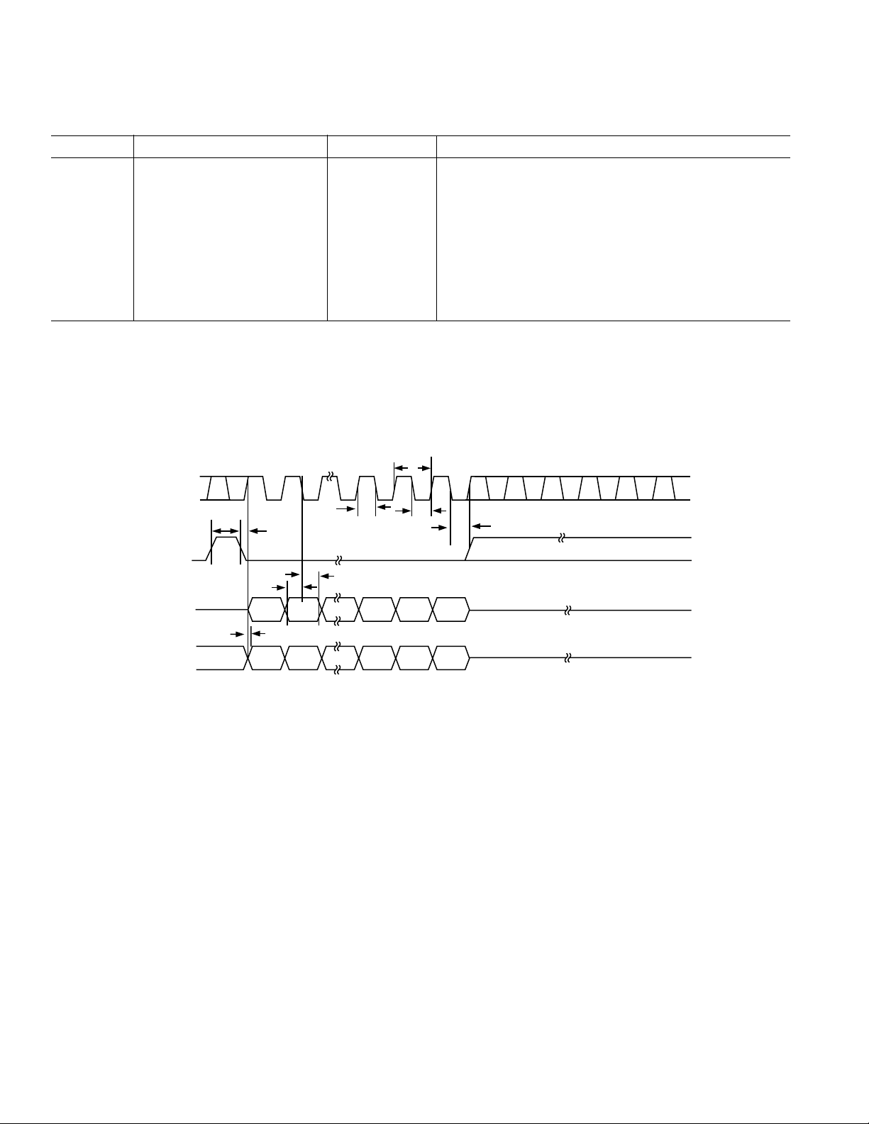
TIMING CHARACTERISTICS
1, 2
(VDD = 2.7 V to 5.5 V. All specifications –40ⴗC to +85ⴗC, unless otherwise noted.)
Parameter Limit at T
f
SCLK
t
1
t
2
t
3
t
4
t
5
t
6
t
7
t
8
3
t
9
NOTES
1
See Figure 1.
2
All input signals are specified with tr = tf = 5 ns (10% to 90% of VDD) and timed from a voltage level of (VIL + VIH)/2.
3
CL = 20 pF, RL = 1 kΩ.
Specifications subject to change without notice.
30 MHz max SCLK Cycle Frequency
33 ns min SCLK Cycle Time
13 ns min SCLK High Time
13 ns min SCLK Low Time
0 ns min SYNC to SCLK Active Edge Setup Time
5 ns min Data Setup Time
4.5 ns min Data Hold Time
0 ns min SCLK Falling Edge to SYNC Rising Edge
33 ns min Minimum SYNC High Time
20 ns min SCLK Rising Edge to DOUT Valid
SCLK
SYNC
, T
MIN
MAX
t
8
t
4
Unit Conditions/Comments
t
1
t
2
t
3
t
7
DIN
DOUT
NOTE
1
DATA FROM LAST WRITE CYCLE
DB7
DB7
t
9
Figure 1. 3-Wire Serial Interface Timing Diagram
t
6
t
5
DB0
1
DB0
1
–4– REV. 0
 Loading...