Analog Devices ADG733 4 a Datasheet

CMOS, 2.5 Low Voltage,
a
FEATURES
1.8 V to 5.5 V Single Supply
2.5 V Dual Supply
2.5 On Resistance
0.5 On Resistance Flatness
100 pA Leakage Currents
19 ns Switching Times
Triple SPDT: ADG733
Quad SPDT: ADG734
Small TSSOP and QSOP Packages
Low Power Consumption
TTL/CMOS Compatible Inputs
APPLICATIONS
Data Acquisition Systems
Communication Systems
Relay Replacement
Audio and Video Switching
Battery Powered Systems
S1B
S1A
S2A
S2B
Triple/Quad SPDT Switches
ADG733/ADG734
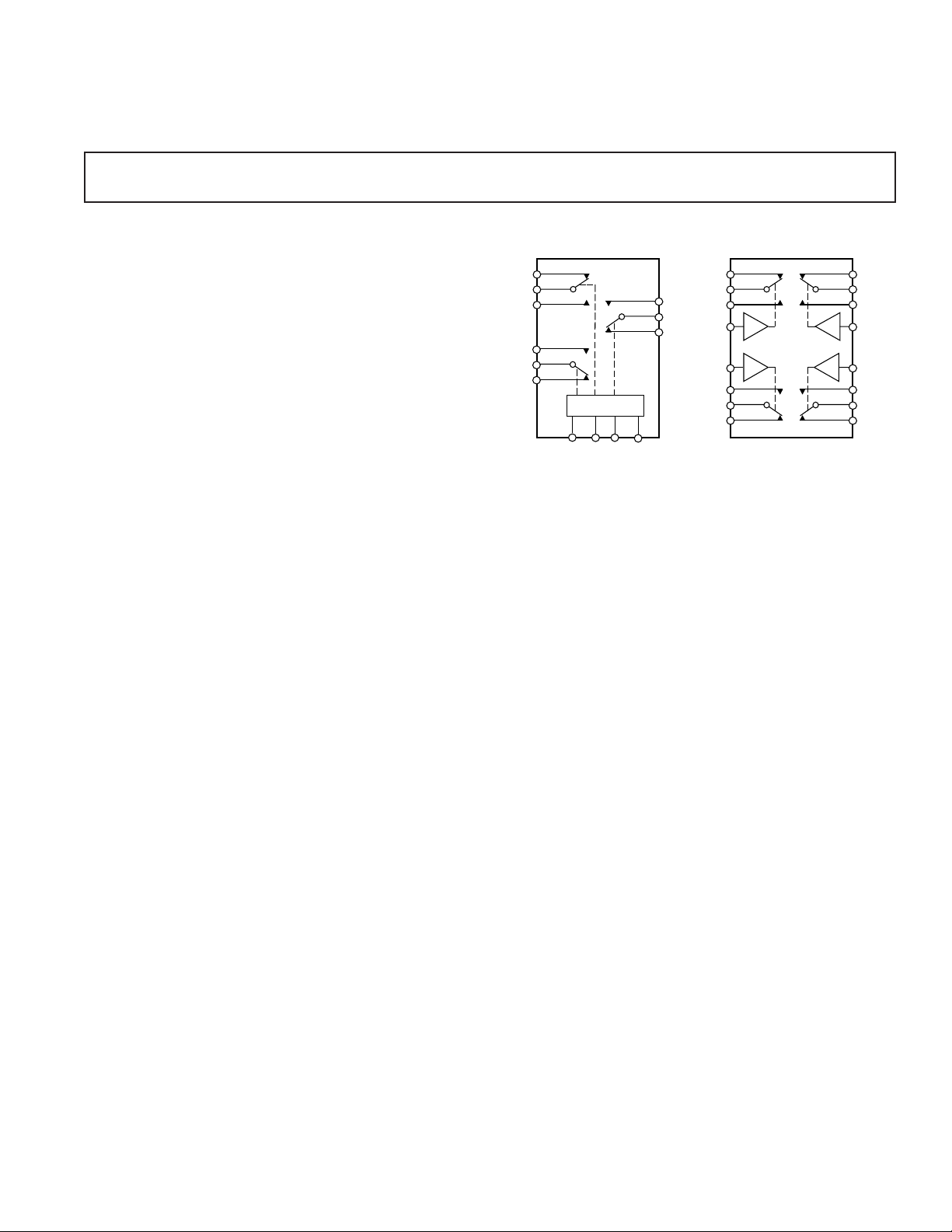
FUNCTIONAL BLOCK DIAGRAMS
ADG733
D1
D2
LOGIC
A2
A0
A1
EN
SWITCHES SHOWN FOR A “1” INPUT LOGIC
S3A
D3
S3B
S1A
S1B
IN1
IN2
S2B
S2A
S4A
D1
ADG734
D2
D2
S4B
IN4
IN3
S3B
D3
S3A
GENERAL DESCRIPTION
The ADG733 and ADG734 are low voltage, CMOS devices
comprising three independently selectable SPDT (single pole,
double throw) switches and four independently selectable SPDT
switches respectively.
Low power consumption and operating supply range of 1.8 V to
5.5 V and dual ±2.5 V make the ADG733 and ADG734 ideal for
battery powered, portable instruments. All channels exhibit
break-before-make switching action preventing momentary
shorting when switching channels. An EN input on the ADG733 is
used to enable or disable the device. When disabled, all channels
are switched OFF.
These 2–1 multiplexers/SPDT switches are designed on an
enhanced submicron process that provides low power dissipation
yet gives high switching speed, very low on resistance, high signal
bandwidths, and low leakage currents. On resistance is in the
region of a few ohms, is closely matched between switches, and is
very flat over the full signal range. These parts can operate equally
well in either direction and have an input signal range that extends
to the supplies.
The ADG733 is available in small TSSOP and QSOP packages,
while the ADG734 is available in a small TSSOP package.
PRODUCT HIGHLIGHTS
1. Single/Dual Supply Operation. The ADG733 and ADG734 are
fully specified and guaranteed with 3 V and 5 V single supply
rails and ±2.5 V dual supply rails.
2. Low On Resistance (2.5 Ω typical)
3. Low Power Consumption (<0.01 µW)
4. Guaranteed Break-Before-Make Switching Action
REV. A
Information furnished by Analog Devices is believed to be accurate and
reliable. However, no responsibility is assumed by Analog Devices for its
use, nor for any infringements of patents or other rights of third parties that
may result from its use. No license is granted by implication or otherwise
under any patent or patent rights of Analog Devices.
One Technology Way, P.O. Box 9106, Norwood, MA 02062-9106, U.S.A.
Tel: 781/329-4700 www.analog.com
Fax: 781/326-8703 © Analog Devices, Inc., 2002

1
ADG733/ADG734–SPECIFICATIONS
(VDD = 5 V 10%, VSS = 0 V, GND = 0 V, unless otherwise noted.)
B Version
–40C
Parameter +25C to +85C Unit Test Conditions/Comments
ANALOG SWITCH
Analog Signal Range 0 V to V
On Resistance (R
) 2.5 Ω typ VS = 0 V to VDD, IDS = 10 mA;
ON
DD
V
4.5 5.0 Ω max Test Circuit 1
On Resistance Match between 0.1 Ω typ V
Channels (∆R
On Resistance Flatness (R
) 0.4 Ω max
ON
FLAT(ON)
) 0.5 Ω typ VS = 0 V to VDD, IDS = 10 mA
= 0 V to VDD, IDS = 10 mA
S
1.2 Ω max
LEAKAGE CURRENTS V
Source OFF Leakage I
(OFF) ± 0.01 nA typ VD = 4.5 V/1 V, VS = 1 V/4.5 V;
S
= 5.5 V
DD
± 0.1 ± 0.3 nA max Test Circuit 2
Channel ON Leakage I
, IS (ON) ±0.01 nA typ VD = VS = 1 V, or 4.5 V;
D
± 0.1 ± 0.5 nA max Test Circuit 3
DIGITAL INPUTS
Input High Voltage, V
Input Low Voltage, V
INL
INH
2.4 V min
0.8 V max
Input Current
I
INL
or I
INH
0.005 µA typ VIN = V
INL
or V
INH
± 0.1 µA max
CIN, Digital Input Capacitance 4 pF typ
DYNAMIC CHARACTERISTICS
t
ON
t
OFF
ADG733 t
(EN)20 ns typ RL = 300 Ω, CL = 35 pF;
ON
t
(EN)7 ns typ RL = 300 Ω, CL = 35 pF;
OFF
Break-Before-Make Time Delay, t
Charge Injection ± 3pC typ V
2
19 ns typ RL = 300 Ω, CL = 35 pF;
34 ns max V
= 3 V, Test Circuit 4
S
7 ns typ RL = 300 Ω, CL = 35 pF;
12 ns max V
40 ns max V
12 ns max V
D
13 ns typ RL = 300 Ω, CL = 35 pF;
1 ns min V
= 3 V, Test Circuit 4
S
= 3 V, Test Circuit 5
S
= 3 V, Test Circuit 5
S
= 3 V, Test Circuit 6
S
= 2 V, RS = 0 Ω, CL = 1 nF;
S
Test Circuit 7
Off Isolation –72 dB typ R
= 50 Ω, CL = 5 pF, f = 1 MHz;
L
Test Circuit 8
Channel-to-Channel Crosstalk –67 dB typ R
= 50 Ω, CL = 5 pF, f = 1 MHz;
L
Test Circuit 9
–3 dB Bandwidth 160 MHz typ R
(OFF) 11 pF typ f = 1 MHz
C
S
= 50 Ω, CL = 5 pF, Test Circuit 10
L
CD, CS (ON) 34 pF typ f = 1 MHz
POWER REQUIREMENTS V
I
DD
0.001 µA typ Digital Inputs = 0 V or 5.5 V
= 5.5 V
DD
1.0 µA max
NOTES
1
Temperature range is as follows: B Version: –40°C to +85°C.
2
Guaranteed by design, not subject to production test.
Specifications subject to change without notice.
–2–
REV. A

1
ADG733/ADG734
SPECIFICATIONS
Parameter +25C to +85C Unit Test Conditions/Comments
ANALOG SWITCH
Analog Signal Range 0 V to V
On Resistance (R
On Resistance Match between 0.1 Ω typ V
Channels (∆R
On Resistance Flatness (R
LEAKAGE CURRENTS V
Source OFF Leakage I
Channel ON Leakage I
DIGITAL INPUTS
Input High Voltage, V
Input Low Voltage, V
Input Current
or I
I
INL
INH
CIN, Digital Input Capacitance 4 pF typ
DYNAMIC CHARACTERISTICS
t
ON
t
OFF
ADG733 t
t
ON
OFF
Break-Before-Make Time Delay, t
Charge Injection ± 3pC typ V
Off Isolation –72 dB typ R
Channel-to-Channel Crosstalk –67 dB typ R
–3 dB Bandwidth 160 MHz typ R
(OFF) 11 pF typ f = 1 MHz
C
S
CD, CS (ON) 34 pF typ f = 1 MHz
POWER REQUIREMENTS V
I
DD
NOTES
1
Temperature ranges are as follows: B Version: –40°C to +85°C.
2
Guaranteed by design, not subject to production test.
Specifications subject to change without notice.
)6 Ω typ VS = 0 V to VDD, IDS = 10 mA;
ON
) 0.4 Ω max
ON
(OFF) ± 0.01 nA typ VS = 3 V/1 V, VD = 1 V/3 V;
S
, IS (ON) ±0.01 nA typ VS = VD = 1 V or 3 V;
D
INH
INL
(EN)29 ns typ RL = 300 Ω, CL = 35 pF;
(EN)9 ns typ RL = 300 Ω, CL = 35 pF;
(VDD = 3 V 10%, VSS = 0 V, GND = 0 V, unless otherwise noted.)
B Version
–40C
V
DD
11 12 Ω max Test Circuit 1
FLAT(ON)
)3Ω typ VS = 0 V to VDD, IDS = 10 mA
± 0.1 ± 0.3 nA max Test Circuit 2
± 0.1 ± 0.5 nA max Test Circuit 3
2.0 V min
0.8 V max
0.005 µA typ VIN = V
± 0.1 µA max
2
28 ns typ RL = 300 Ω, CL = 35 pF;
55 ns max V
9 ns typ RL = 300 Ω, CL = 35 pF;
16 ns max V
60 ns max V
16 ns max V
D
22 ns typ RL = 300 Ω, CL = 35 pF;
1 ns min V
0.001 µA typ Digital Inputs = 0 V or 3.3 V
1.0 µA max
= 0 V to VDD, IDS = 10 mA
S
= 3.3 V
DD
or V
INL
= 2 V, Test Circuit 4
S
= 2 V, Test Circuit 4
S
= 2 V, Test Circuit 5
S
= 2 V, Test Circuit 5
S
= 2 V, Test Circuit 6
S
= 1 V, RS = 0 Ω, CL = 1 nF;
S
INH
Test Circuit 7
= 50 Ω, CL = 5 pF, f = 1 MHz;
L
Test Circuit 8
= 50 Ω, CL = 5 pF, f = 1 MHz;
L
Test Circuit 9
= 50 Ω, CL = 5 pF, Test Circuit 10
L
= 3.3 V
DD
REV. A
–3–

ADG733/ADG734–SPECIFICATIONS
1
DUAL SUPPLY
(VDD = +2.5 V 10%, VSS = –2.5 V 10%, GND = 0 V, unless otherwise noted.)
B Version
–40C
Parameter +25C to +85C Unit Test Conditions/Comments
ANALOG SWITCH
Analog Signal Range V
On Resistance (R
) 2.5 Ω typ VS = VSS to VDD, IDS = 10 mA;
ON
SS
to V
DD
V
4.5 5.0 Ω max Test Circuit 1
On Resistance Match between 0.1 Ω typ V
Channels (∆R
On Resistance Flatness (R
) 0.4 Ω max
ON
FLAT(ON)
) 0.5 Ω typ VS = VSS to VDD, IDS = 10 mA
= VSS to VDD, IDS = 10 mA
S
1.2 Ω max
LEAKAGE CURRENTS V
Source OFF Leakage I
(OFF) ± 0.01 nA typ
S
= +2.75 V, VSS = –2.75 V
DD
VS = +2.25 V/–1.25 V, VD = –1.25 V/+2.25 V;
± 0.1 ± 0.3 nA max Test Circuit 2
Channel ON Leakage I
, IS (ON) ±0.01 nA typ
D
VS = VD = +2.25 V/–1.25 V, Test Circuit 3
± 0.1 ± 0.5 nA max
DIGITAL INPUTS
Input High Voltage, V
Input Low Voltage, V
INL
INH
1.7 V min
0.7 V max
Input Current
I
INL
or I
INH
0.005 µA typ VIN = V
INL
or V
INH
± 0.1 µA max
CIN, Digital Input Capacitance 4 pF typ
DYNAMIC CHARACTERISTICS
t
ON
t
OFF
ADG733 t
(EN)21 ns typ RL = 300 Ω, CL = 35 pF;
ON
t
(EN)10 ns typ RL = 300 Ω, CL = 35 pF;
OFF
Break-Before-Make Time Delay, t
Charge Injection ± 5pC typ V
2
21 ns typ RL = 300 Ω, CL = 35 pF;
35 ns max V
= 1.5 V, Test Circuit 4
S
10 ns typ RL = 300 Ω, CL = 35 pF;
16 ns max V
40 ns max V
16 ns max V
D
13 ns typ RL = 300 Ω, CL = 35 pF;
1 ns min V
= 1.5 V, Test Circuit 4
S
= 1.5 V, Test Circuit 5
S
= 1.5 V, Test Circuit 5
S
= 1.5 V, Test Circuit 6
S
= 0 V, RS = 0 Ω, CL = 1 nF;
S
Test Circuit 7
Off Isolation –72 dB typ R
= 50 Ω, CL = 5 pF, f = 1 MHz;
L
Test Circuit 8
Channel-to-Channel Crosstalk –67 dB typ R
= 50 Ω, CL = 5 pF, f = 1 MHz;
L
Test Circuit 9
–3 dB Bandwidth 200 MHz typ R
(OFF) 11 pF typ f = 1 MHz
C
S
= 50 Ω, CL = 5 pF, Test Circuit 10
L
CD, CS (ON) 34 pF typ f = 1 MHz
POWER REQUIREMENTS V
I
DD
0.001 µA typ Digital Inputs = 0 V or 2.75 V
= 2.75 V
DD
1.0 µA max
I
SS
0.001 µA typ VSS = –2.75 V
1.0 µA max Digital Inputs = 0 V or 2.75 V
NOTES
1
Temperature range is as follows: B Version: –40°C to +85°C.
2
Guaranteed by design, not subject to production test.
Specifications subject to change without notice.
–4–
REV. A
 Loading...