

16-/32-Channel, 4
ADG732
EN
S1
S32
WR
CS
A4A3A2A1A0
D
1-OF-32
DECODER
S1A
S16A
DA
ADG726
EN
WR
A3A2A1A0
S1B
S16B
DB
1-OF-16
DECODER
CSA
CSB
www.BDTIC.com/ADI
a
FEATURES
1.8 V to 5.5 V Single Supply
2.5 V Dual-Supply Operation
4 On Resistance
0.5 On Resistance Flatness
48-Lead TQFP or 48-Lead 7 mm 7 mm CSP Packages
Rail-to-Rail Operation
30 ns Switching Times
Single 32-to-1 Channel Multiplexer
Dual/Differential 16-to-1 Channel Multiplexer
TTL/CMOS Compatible Inputs
For Functionally Equivalent Devices with Serial Interface
See ADG725/ADG731
APPLICATIONS
Optical Applications
Data Acquisition Systems
Communication Systems
Relay Replacement
Audio and Video Switching
Battery-Powered Systems
Medical Instrumentation
Automatic Test Equipment
+1.8 V to +5.5 V, 2.5 V Analog Multiplexers
ADG726/ADG732
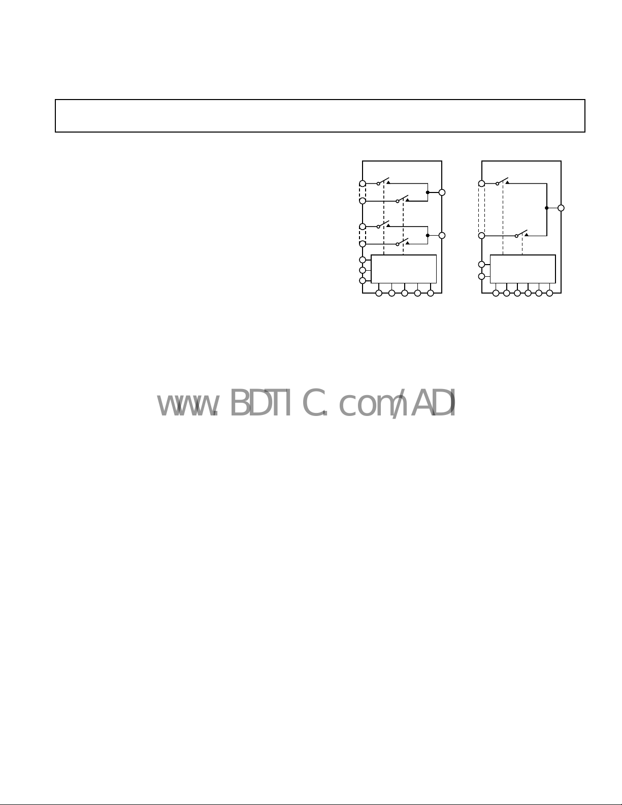
FUNCTIONAL BLOCK DIAGRAMS
GENERAL DESCRIPTION
The ADG726/ADG732 are monolithic CMOS 32-channel/dual
16-channel analog multiplexers. The ADG732 switches one of
32 inputs (S1-S32) to a common output, D, as determined by
the 5-bit binary address lines A0, A1, A2, A3, and A4. The
ADG726 switches one of 16 inputs as determined by the 4-bit
binary address lines A0, A1, A2, and A3.
On-chip latches facilitate microprocessor interfacing. The
ADG726 device may also be configured for differential operation by tying CSA and CSB together. An EN input is used to
enable or disable the devices. When disabled, all channels are
switched OFF.
These multiplexers are designed on an enhanced submicron
process that provides low power dissipation yet gives high
switching speed, very low on resistance, and leakage currents.
They operate from a single supply of +1.8 V to +5.5 V and a ±2.5 V
dual supply, making them ideally suited to a variety of applications.
On resistance is in the region of a few ohms and is closely
matched between switches and very flat over the full signal
range. These parts can operate equally well as either multiplexers
or demultiplexers and have an input signal range that extends to
the supplies. In the OFF condition, signal levels up to the supplies
are blocked. All channels exhibit break-before-make switching
action, preventing momentary shorting when switching channels.
They are available in either 48-lead CSP or TQFP packages.
REV. 0
Information furnished by Analog Devices is believed to be accurate and
reliable. However, no responsibility is assumed by Analog Devices for its
use, nor for any infringements of patents or other rights of third parties that
may result from its use. No license is granted by implication or otherwise
under any patent or patent rights of Analog Devices.
PRODUCT HIGHLIGHTS
1. +1.8 V to +5.5 V single- or ±2.5 V dual-supply operation.
These parts are specified and guaranteed with +5 V ± 10%,
+3 V ± 10% single-supply, and ±2.5 V ± 10% dualsupply rails.
2. On resistance of 4 Ω
3. Guaranteed break-before-make switching action
4. 7 mm × 7 mm 48-lead chip scale package (CSP)
or 48-lead TQFP package
One Technology Way, P.O. Box 9106, Norwood, MA 02062-9106, U.S.A.
Tel: 781/329-4700 www.analog.com
Fax: 781/326-8703 © Analog Devices, Inc., 2002
ADG726/ADG732–SPECIFICATIONS
www.BDTIC.com/ADI
1
(VDD = 5 V 10%, V
= 0 V, GND = 0 V, unless otherwise noted.)
SS
B Version
–40C
Parameter +25C to +85CUnit Test Conditions/Comments
ANALOG SWITCH
Analog Signal Range 0 V to V
On Resistance (R
)4 Ω typ VS = 0 V to VDD, IDS = 10 mA;
ON
DD
V
5.5 6 Ω max Test Circuit 1
On Resistance Match Between 0.3 Ω typ VS = 0 V to VDD, IDS = 10 mA
Channels (∆R
On Resistance Flatness (R
) 0.8 Ω max
ON
) 0.5 Ω typ VS = 0 V to VDD, IDS = 10 mA
FLAT(ON)
1Ω max
LEAKAGE CURRENTS V
Source OFF Leakage I
(OFF) ± 0.01 nA typ VD = 4.5 V/1 V, VS = 1 V/4.5 V;
S
= 5.5 V
DD
± 0.25 ± 1 nA max Test Circuit 2
Drain OFF Leakage I
(OFF) ± 0.05 nA typ VD = 4.5 V/1 V, VS = 1 V/4.5 V;
D
ADG726 ± 0.5 ± 2.5 nA max Test Circuit 3
ADG732 ± 1 ± 5 nA max
Channel ON Leakage I
, IS (ON) ± 0.05 nA typ VD = VS = 1 V, or 4.5 V;
D
ADG726 ± 0.5 ± 2.5 nA max Test Circuit 4
ADG732 ± 1 ± 5 nA max
DIGITAL INPUTS
Input High Voltage, V
Input Low Voltage, V
INL
INH
2.4 V min
0.8 V max
Input Current
I
INL
or I
INH
0.005 µA typ VIN = V
INL
or V
INH
± 0.5 µA max
CIN, Digital Input Capacitance 5 pF typ
DYNAMIC CHARACTERISTICS
t
TRANSITION
Break-Before-Make Time Delay, t
2
23 ns typ RL = 300 Ω, CL = 35 pF, Test Circuit 5
34 40 ns max VS1 = 3 V/0 V, V
D
18 ns typ RL = 300 Ω, CL = 35 pF;
= 0 V/3 V
S32
1 ns min VS = 3 V; Test Circuit 6
tON(CS, WR)18ns typ VS = 3 V; Test Circuit 7
25 32 ns max RL = 300 Ω, CL = 35 pF;
t
(CS, WR)17ns typ VS = 3 V; Test Circuit 7
OFF
23 29 ns max RL = 300 Ω, CL = 35 pF;
tON(EN)24ns typ RL = 300 Ω, CL = 35 pF;
t
32 40 ns max V
(EN)16ns typ RL = 300 Ω, CL = 35 pF;
OFF
= 3 V; Test Circuit 8
S
22 25 ns max VS = 3 V; Test Circuit 8
Charge Injection 5 pC typ V
= 2.5 V, RS = 0 Ω, CL = 1 nF;
S
Test Circuit 9
OFF Isolation –72 dB typ RL = 50 Ω, CL = 5 pF, f = 1 MHz;
Test Circuit 10
Channel-to-Channel Crosstalk –72 dB typ R
= 50 Ω, CL = 5 pF, f = 1 MHz;
L
Test Circuit 11
–3 dB Bandwidth R
= 50 Ω, CL = 5 pF; Test Circuit 12
L
ADG726 34 MHz typ
ADG732 18 MHz typ
C
(OFF) 13 pF typ f = 1 MHz
S
CD (OFF)
ADG726 170 pF typ f = 1 MHz
ADG732 340 pF typ f = 1 MHz
C
, CS (ON)
D
ADG726 175 pF typ f = 1 MHz
ADG732 350 pF typ f = 1 MHz
POWER REQUIREMENTS VDD = 5.5 V
I
DD
10 µA typ Digital Inputs = 0 V or 5.5 V
20 µA max
NOTES
1
Temperature range is as follows: B Version: –40°C to +85°C.
2
Guaranteed by design; not subject to production test.
Specifications subject to change without notice.
–2–
REV. 0
ADG726/ADG732
www.BDTIC.com/ADI
SPECIFICATIONS
Parameter +25C to +85CUnit Test Conditions/Comments
ANALOG SWITCH
Analog Signal Range 0 V to V
On Resistance (RON)7 Ω typ VS = 0 V to VDD, IDS = 10 mA;
On Resistance Match Between 0.35 Ω typ V
Channels (∆RON)1Ω max
On Resistance Flatness (R
LEAKAGE CURRENTS V
Source OFF Leakage I
Drain OFF Leakage I
ADG726 ± 0.5 ± 2.5 nA max Test Circuit 3
ADG732 ± 1 ± 5 nA max
Channel ON Leakage I
ADG726 ± 0.5 ± 2.5 nA max Test Circuit 4
ADG732 ± 1 ± 5 nA max
DIGITAL INPUTS
Input High Voltage, V
Input Low Voltage, V
Input Current
I
or I
INL
INH
CIN, Digital Input Capacitance 5 pF typ
DYNAMIC CHARACTERISTICS
t
TRANSITION
Break-Before-Make Time Delay, t
tON(WR, CS)29ns typ VS = 2 V; Test Circuit 7
t
(WR, CS)26ns typ VS = 2 V; Test Circuit 7
OFF
t
(EN, WR)33ns typ RL = 300 Ω, CL = 35 pF;
ON
t
(EN)19ns typ RL = 300 Ω, CL = 35 pF;
OFF
Charge Injection 1 pC typ VS = 1.5 V, RS = 0 Ω, CL = 1 nF;
Off Isolation –72 dB typ R
Channel-to-Channel Crosstalk –72 dB typ RL = 50 Ω, CL = 5 pF, f = 1 MHz;
–3 dB Bandwidth R
ADG726 34 MHz typ
ADG732 18 MHz typ
C
(OFF) 13 pF typ f = 1 MHz
S
CD (OFF)
ADG726 170 pF typ f = 1 MHz
ADG732 340 pF typ f = 1 MHz
C
, CS (ON)
D
ADG726 175 pF typ f = 1 MHz
ADG732 350 pF typ f = 1 MHz
POWER REQUIREMENTS VDD = 3.3 V
I
DD
NOTES
1
Temperature ranges are as follows: B Version: –40°C to +85°C.
2
Guaranteed by design; not subject to production test.
Specifications subject to change without notice.
FLAT(ON)
(OFF) ± 0.01 nA typ VS = 3 V/1 V, VD = 1 V/3 V;
S
(OFF) ± 0.05 nA max VS = 1 V/3 V, VD = 3 V/1 V;
D
, IS (ON) ± 0.05 nA typ VS = VD = 1 V or 3 V;
D
INH
INL
(VDD = 3 V 10%, V
= 0 V, GND = 0 V, unless otherwise noted.)
SS
B Version
–40C
V
DD
11 12 Ω max Test Circuit 1
= 0 V to VDD, IDS = 10 mA
S
)3Ω typ VS = 0 V to VDD, IDS = 10 mA
= 3.3 V
DD
± 0.25 ± 1 nA max Test Circuit 2
2.0 V min
0.7 V max
0.005 µA typ VIN = V
INL
or V
INH
± 0.5 µA max
2
34 ns typ RL = 300 Ω, CL = 35 pF; Test Circuit 5
52 62 ns max VS1 = 2 V/0 V, V
D
26 ns typ RL = 300 Ω, CL = 35 pF;
= 0 V/2 V
S32
1 ns min VS = 2 V; Test Circuit 6
43 52 ns max R
= 300 Ω, CL = 35 pF;
L
38 42 ns max RL = 300 Ω, CL = 35 pF;
48 55 ns max VS = 3 V; Test Circuit 8
25 28 ns max V
= 2 V; Test Circuit 8
S
Test Circuit 9
= 50 Ω, CL = 5 pF, f = 1 MHz;
L
Test Circuit 10
Test Circuit 11
= 50 Ω, CL = 5 pF; Test Circuit 12
L
5 µA typ Digital Inputs = 0 V or 3.3 V
10 µA max
1
REV. 0
–3–
ADG726/ADG732 SPECIFICATIONS
www.BDTIC.com/ADI
1
DUAL SUPPLY
Parameter +25ⴗC to +85ⴗC Unit Test Conditions/Comments
ANALOG SWITCH
Analog Signal Range V
On Resistance (R
On Resistance Match Between 0.3 Ω typ V
Channels (∆RON) 0.8 Ω max
On Resistance Flatness (R
LEAKAGE CURRENTS VDD = +2.75 V, VSS = –2.75 V
Source OFF Leakage IS (OFF) ±0.01 nA typ VS = +2.25 V/–1.25 V, VD = –1.25 V/+2.25 V;
Drain OFF Leakage ID (OFF) ±0.05 nA max VS = +2.25 V/–1.25 V, VD = –1.25 V/+2.25 V;
ADG726 ± 0.5 ±2.5 nA max Test Circuit 3
ADG732 ± 1 ± 5 nA max
Channel ON Leakage ID, IS (ON) ±0.05 nA typ VS = VD = +2.25 V/–1.25 V;
ADG726 ± 0.5 ±2.5 nA max Test Circuit 4
ADG732 ± 1 ± 5 nA max
DIGITAL INPUTS
Input High Voltage, V
Input Low Voltage, V
Input Current
I
or I
INL
INH
CIN, Digital Input Capacitance 5 pF typ
DYNAMIC CHARACTERISTICS
t
TRANSITION
Break-Before-Make Time Delay, t
tON(CS, WR) 21 ns typ VS = 1.5 V; Test Circuit 7
t
(CS, WR) 20 ns typ VS = 1.5 V; Test Circuit 7
OFF
tON(EN, WR) 26 ns typ RL = 300 ⍀, CL = 35 pF;
t
(EN) 18 ns typ RL = 300 ⍀, CL = 35 pF;
OFF
Charge Injection 1 pC typ VS = 0 V, RS = 0 ⍀, CL = 1 nF;
OFF Isolation –72 dB typ RL = 50 ⍀, CL = 5 pF, f = 1 MHz;
Channel-to-Channel Crosstalk –72 dB typ RL = 50 ⍀, CL = 5 pF, f = 1 MHz;
–3 dB Bandwidth RL = 50 ⍀, CL = 5 pF; Test Circuit 12
ADG726 34 MHz typ
ADG732 18 MHz typ
CS (OFF) 13 pF typ
CD (OFF)
ADG726 137 pF typ f = 1 MHz
ADG732 275 pF typ f = 1 MHz
CD, CS (ON)
ADG726 150 pF typ f = 1 MHz
ADG732 300 pF typ f = 1 MHz
POWER REQUIREMENTS
I
DD
I
SS
NOTES
1
Temperature range is as follows: B Version: –40°C to +85°C.
2
Guaranteed by design; not subject to production test.
Specifications subject to change without notice.
(VDD = +2.5 V ⴞ 10%, V
)4 Ω typ VS = VSS to VDD, IDS = 10 mA;
ON
) 0.5 Ω typ VS = VSS to VDD, IDS = 10 mA
FLAT(ON)
INH
INL
2
D
= –2.5 V ⴞ 10%, GND = 0 V, unless otherwise noted.)
SS
B Version
–40ⴗC
to V
SS
DD
5.5 6 Ω max Test Circuit 1
1 Ω max
± 0.25 ± 0.5 nA max Test Circuit 2
1.7 V min
0.7 V max
0.005 µA typ VIN = V
33 ns typ RL = 300 ⍀, CL = 35 pF; Test Circuit 5
45 51 ns max VS1 = 1.5 V/0 V, V
15 ns typ RL = 300 ⍀, CL = 35 pF;
1 ns min VS = 1.5 V; Test Circuit 6
30 37 ns max RL = 300 ⍀, CL = 35 pF;
29 35 ns max RL = 300 ⍀, CL = 35 pF;
37 ns max VS = 1.5 V; Test Circuit 8
26 29 ns max VS = 1.5 V; Test Circuit 8
10 µA typ VDD = +2.75 V
10 µA typ VSS = –2.75 V
± 0.5 µA max
20 µA max Digital Inputs = 0 V or +2.75 V
20 µA max Digital Inputs = 0 V or +2.75 V
V
= VSS to VDD, IDS = 10 mA
S
or V
INL
INH
= 0 V/1.5 V
S32
Test Circuit 9
Test Circuit 10
Test Circuit 11
–4–
REV. 0

ADG726/ADG732
www.BDTIC.com/ADI
TIMING CHARACTERISTICS
Parameter Limit at T
t
1
t
2
t
3
t
4
t
5
t
6
NOTES
1
See Figure 1.
2
All input signals are specified with tr = tf = 1 ns (10% to 90% of VDD).
3
Guaranteed by design and characterization, not production tested.
Specifications subject to change without notice.
0 ns min CS to WR Setup Time
0 ns min CS to WR Hold Time
10 ns min WR Pulsewidth
10 ns min Time between WR Cycles
5 ns min Address, Enable Setup Time
2 ns min Address, Enable Hold Time
MIN
, T
1, 2, 3
MAX
CS
WR
A0, A1, A2, A3, (A4)
EN
Unit Conditions/Comments
t
1
t
3
t
5
t
2
t
4
t
6
Figure 1. Timing Diagram
Figure 1 shows the timing sequence for latching the switch
address and enable inputs. The latches are level sensitive; there-
fore, while WR is held low, the latches are transparent and the
switches respond to changing the address and enable the inputs.
Input data is latched on the rising edge of WR. The ADG726
has two CS inputs. This enables the part to be used either as a
dual 16-1 channel multiplexer or a differential 16-channel
multiplexer. If a differential output is required, tie CSA and
CSB together.
REV. 0
–5–

ADG726/ADG732
www.BDTIC.com/ADI
ABSOLUTE MAXIMUM RATINGS
1
(TA = 25°C, unless otherwise noted.)
VDD to VSS . . . . . . . . . . . . . . . . . . . . . . . . . . . . . . . . . . . . . . 7 V
V
to GND . . . . . . . . . . . . . . . . . . . . . . . . . . . –0.3 V to +7 V
DD
to GND . . . . . . . . . . . . . . . . . . . . . . . . . . . . +0.3 V to –7 V
V
SS
Analog Inputs
Digital Inputs
2
. . . . . . . . . . . . . . VSS – 0.3 V to VDD + 0.3 V or
2
. . . . . . . . . . . . . . . . . . –0.3 V to VDD + 0.3 V or
30 mA, Whichever Occurs First
30 mA, Whichever Occurs First
Peak Current, S or D . . . . . . . . . . . . . . . . . . . . . . . . . . . 60 mA
(Pulsed at 1 ms, 10% Duty Cycle Max)
Continuous Current, S or D . . . . . . . . . . . . . . . . . . . . . 30 mA
Operating Temperature Range
Industrial (B Version) . . . . . . . . . . . . . . . . . –40°C to +85°C
ORDERING GUIDE
Model Temperature Range Package Description Package Option
ADG726BCP –40°C to +85°CChip Scale Package (LPCSP) CP-48
ADG726BSU –40°C to +85°CThin Quad Flatpack (TQFP) SU-48
ADG732BCP –40°C to +85°CChip Scale Package (LPCSP) CP-48
ADG732BSU –40°C to +85°CThin Quad Flatpack (TQFP) SU-48
Storage Temperature Range . . . . . . . . . . . . –65°C to +150°C
Junction Temperature . . . . . . . . . . . . . . . . . . . . . . . . . . 150°C
Thermal Impedence (Four-layer board)
48-Lead LFCSP . . . . . . . . . . . . . . . . . . . . . . . . . . . 25⬚C/W
48-Lead TQFP . . . . . . . . . . . . . . . . . . . . . . . . . . . 54.6⬚C/W
Lead Temperature, Soldering (10 sec) . . . . . . . . . . . . . 300°C
IR Reflow, Peak Temperature (<20 sec) . . . . . . . . . . . . 235°C
NOTES
1
Stresses above those listed under Absolute Maximum Ratings may cause permanent damage to the device. This is a stress rating only and functional operation of
the device at these or any other conditions above those listed in the operational
sections of this specification is not implied. Exposure to absolute maximum rating
conditions for extended periods may affect device reliability. Only one absolute
maximum rating may be applied at any one time.
2
Overvoltages at A, EN, WR, CS, S, or D will be clamped by internal diodes.
Current should be limited to the maximum ratings given.
CAUTION
ESD (electrostatic discharge) sensitive device. Electrostatic charges as high as 4000 V readily
accumulate on the human body and test equipment and can discharge without detection.
Although the ADG726/ADG732 features proprietary ESD protection circuitry, permanent damage
may occur on devices subjected to high energy electrostatic discharges. Therefore, proper ESD
precautions are recommended to avoid performance degradation or loss of functionality.
PIN CONFIGURATIONS
LFCSP and TQFP
40 S32
39 S31
38 S30
S12
S11
S10
S9
S8
S7
S6
S5
S4
S3
10
11
S2
S1
12
NC = NO CONNECT
48 S13
47 S14
46 S15
45 S16
44 NC
43 D
42 NC
1
2
3
4
5
6
7
8
9
PIN 1
INDICATOR
14
13
DD
DD
V
V
ADG732
TOP VIEW
A0 15
A1 16
A3 18
A2 17
A4 19
41 NC
CS 20
WR 21
EN 22
GND 23
37 S29
24
SS
V
36 S28
35 S27
34 S26
33 S25
32 S24
31 S23
30 S22
29 S21
28 S20
27 S19
26 S18
25 S17
S12A
S11A
S10A
S9A
S8A
S7A
S6A
S5A
S4A
S3A
S2A
S1A
NC = NO CONNECT
48 S13A
47 S14A
46 S15A
45 S16A
44 NC
1
2
3
4
5
6
7
8
9
10
11
12
PIN 1
INDICATOR
14
13
DD
DD
V
V
ADG726
TOP VIEW
A0 15
A1 16
A2 17
43 DA
A3 18
42 NC
41 DB
CSA 19
CSB 20
WARNING!
40 S16B
39 S15B
38 S14B
37 S13B
24
SS
EN 22
WR 21
V
GND 23
ESD SENSITIVE DEVICE
36 S12B
35 S11B
34 S10B
33 S9B
32 S8B
31 S7B
30 S6B
29 S5B
28 S4B
27 S3B
26 S2B
25 S1B
–6–
REV. 0

ADG726/ADG732
www.BDTIC.com/ADI
Table I. ADG726 Truth Table
A3 A2 A1 A0 EN CSA CSB WR ON Switch
X XXX X 11L->H Retains Previous Switch Condition
X XXX X 11XNo Change in Switch Condition
X XXX 1 000 NONE
00000000 S1A–DA, S1B–DB
00010000 S2A–DA, S2B–DB
00100000 S3A–DA, S3B–DB
00110000 S4A–DA, S4B–DB
01000000 S5A–DA, S5B–DB
01010000 S6A–DA, S6B–DB
01100000 S7A–DA, S7B–DB
01110000 S8A–DA, S8B–DB
10000000 S9A–DA, S9B–DB
1 001 0 000 S10A–DA, S10B–DB
1 010 0 000 S11A–DA, S11B–DB
1 011 0 000 S12A–DA, S12B–DB
1 100 0 000 S13A–DA, S13B–DB
1 101 0 000 S14A–DA, S14B–DB
1 110 0 000 S15A–DA, S15B–DB
1 111 0 000 S16A–DA, S16B–DB
X = Don’t Care
Table II. ADG732 Truth Table
A4 A3 A2 A1 A0 EN CS WR Switch Condition
X XXX XX 1 L->H Retains Previous Switch Condition
X XXX XX 1XNo Change in Switch Condition
X XXX X 100 NONE
00000000 1
00001000 2
00010000 3
00011000 4
00100000 5
00101000 6
00110000 7
00111000 8
01000000 9
01001000 10
01010000 11
01011000 12
01100000 13
01101000 14
01110000 15
01111000 16
10000000 17
10001000 18
10010000 19
10011000 20
10100000 21
10101000 22
10110000 23
10111000 24
11000000 25
11001000 26
11010000 27
11011000 28
11100000 29
11101000 30
11110000 31
11111000 32
X = Don’t Care
REV. 0
–7–

ADG726/ADG732
www.BDTIC.com/ADI
TERMINOLOGY
V
DD
V
SS
I
DD
I
SS
GND Ground (0 V) Reference
S Source Terminal. May be an input or output.
DDrain Terminal. May be an input or output.
IN Logic Control Input
)Analog Voltage on Terminals D and S
V
D (VS
R
ON
∆R
ON
R
FLAT(ON)
(OFF) Source Leakage Current with the Switch OFF
I
S
(OFF) Drain Leakage Current with the Switch OFF
I
D
, IS (ON) Channel Leakage Current with the Switch ON
I
D
V
INL
V
INH
I
INL(IINH
C
C
C
C
t
TRANSITION
t
ON
t
OFF
t
OPEN
) Input Current of the Digital Input
(OFF) OFF Switch Source Capacitance. Measured with reference to ground.
S
(OFF) OFF Switch Drain Capacitance. Measured with reference to ground.
D
(ON) ON Switch Capacitance. Measured with reference to ground.
D,CS
IN
(EN)Delay Time between the 50% and 90% Points of the EN Digital Input and the Switch ON Condition
(EN)Delay Time between the 50% and 90% Points of the EN Digital Input and the Switch OFF Condition
Charge A Measure of the Glitch Impulse Transferred from the Digital Input to the Analog Output During Switching
Injection
OFF Isolation A Measure of Unwanted Signal Coupling through an OFF Switch
Crosstalk A Measure of Unwanted Signal Coupling from One Channel to Another as a Result of Parasitic Capacitance
ON Response The Frequency Response of the ON Switch
Insertion The Loss Due to the On Resistance of the Switch
Loss
Most Positive Power Supply Potential
Most Negative Power Supply in a Dual-Supply Application. In single-supply applications, connect to GND.
Positive Supply Current
Negative Supply Current
Ohmic Resistance between D and S
On Resistance Match between any two channels, i.e., RONmax – RONmin
Flatness is defined as the difference between the maximum and minimum value of on resistance as measured
over the specified analog signal range.
Maximum Input Voltage for Logic “0”
Minimum Input Voltage for Logic “1”
Digital Input Capacitance
Delay Time Measured between the 50% and 90% Points of the Digital Inputs and the Switch ON Condition
when Switching from One Address State to Another
OFF Time Measured between the 80% Points of Both Switches when Switching from One Address State to Another
–8–
REV. 0

Typical Performance Characteristics—
www.BDTIC.com/ADI
ADG726/ADG732
8
RESISTANCE –
7
6
5
4
3
2
1
0 5.505.04.54.03.53.02.52.01.51.00.5
VDD = 2.7V
VDD = 3.0V
VDD = 4.5V
VD, VS – V
VDD = 3.3V
T
= +25C
A
= 0V
V
SS
V
= 5.5V
DD
VDD = 5V
TPC 1. On Resistance vs. VD(VS),
Single Supply
8
7
6
5
4
3
RESISTANCE –
2
1
0
0
+25C
+85C
–40C
0.3 0.6 0.9 1.2 1.5 1.8 2.1 2.4 2.7 3.0
VD, VS – V
VSS = 0V
TPC 4. On Resistance vs. VD(VS),
Single Supply
8
7
VDD = +2.25V
6
= –2.25V
V
SS
5
4
3
RESISTANCE –
2
1
0
–1.75 –0.75 0.25 1.25 2.25
–2.75
TA = +25C
V
DD
V
SS
VD, VS – V
= +2.5V
= –2.5V
V
= +2.75V
DD
= –2.75V
V
SS
TPC 2. On Resistance vs. VD(VS),
Dual Supply
8
7
6
5
4
3
RESISTANCE –
2
1
0
–2.0 –1.5 –1.0–0.5 0 0.5 1.0 1.5 2.0 2.5
–2.5
+85C
+25C
–40C
VD, VS – V
TPC 5. On Resistance vs. VD(VS),
Dual Supply
8
7
6
5
4
3
RESISTANCE –
2
1
0
0.5 1.0 1.5 2.0 2.5 3.0 3.5 4.0 4.5 5.0
0
+85C
+25C
–40C
VD, VS – V
VSS = 0V
TPC 3. On Resistance vs. VD(VS)
for Different Temperatures,
Single Supply
CURRENT – nA
0.5
0.4
0.3
0.2
0.1
0
–0.1
–0.2
–0.3
–0.4
–0.5
15 8525 35 45 55 65 75
5
TEMPERATURE – C
VDD = 5V
V
TPC 6. Leakage Currents vs.
Temperature
= 0V
SS
25
20
15
10
5
– pC
INJ
Q
0
–5
–10
–15
–3 –2 5
–1 01234
VD, VS – V
TA = +25C
TPC 7. ADG732 Charge Injection
45
VSS = 0V
40
35
30
25
20
TIME – ns
15
10
5
0
–40 –20 80
TPC 8. tON/t
VDD = 3V
V
t
t
DD
ON
VDD = 5V
OFF
TEMPERATURE – C
Times vs. Temperature
OFF
vs. Source Voltage
REV. 0
= 5V
0204060
VDD = 3V
–9–
1.8
1.6
1.4
1.2
1.0
0.8
0.6
0.4
LOGIC THRESHOLD VOLTAGE – V
0.2
0
01 62345
RISING
FA LL ING
V
– V
DD
TA = 25C
TPC 9. Logic Threshold Voltage
vs. Supply Voltage

ADG726/ADG732
www.BDTIC.com/ADI
0
–10
–20
–30
–40
–50
–60
–70
ATTENUATION – dB
–80
–90
–100
0.03 0.1 1 10 100
FREQUENCY – MHz
VDD = 5V
= 25C
T
A
TPC 10. OFF Isolation vs. Frequency
Test Circuits
V
S
I
DS
V1
SD
RON = V1/I
DS
Test Circuit 1. On Resistance
0
VDD = 3V, 5V
–10
T
= 25C
A
–20
–30
–40
–50
–60
–70
ATTENUATION – dB
–80
–90
–100
0.03 0.1 100110
FREQUENCY – MHz
TPC 11. Crosstalk vs. Frequency
0
VDD = 5V
–2
= 25C
T
A
–4
–6
–8
ATTENUATION – dB
–10
–12
–14
0.03 0.1 1 10 100
TPC 12. ON Response vs. Frequency
VDDV
SS
V
DDVSS
S1
S2
S32
V
S
GND
EN
Test Circuit 3. ID (OFF)
ADG732
FREQUENCY – MHz
ID(OFF)
D
A
LOGIC “1”
ADG726
V
D
VDDV
SS
V
S
IS(OFF)
A
V
S
S32
V
DDVSS
S1
S2
GND
EN
D
LOGIC “1”
V
D
Test Circuit 2. IS (OFF)
V
V
DD
SS
V
V
SS
DD
V
IN
A4
50
A0
ADG732*
CS
EN
*SIMILAR CONNECTION FOR ADG726
S1
S2 THRU S31
S32
GND
WR
V
S1
V
S32
D
R
L
300
C
L
35pF
ADDRESS
DRIVE (V
V
OUT
Test Circuit 5. Switching Time of Multiplexer, t
V
V
SS
DD
V
V
DD
S2 THRU S31
GND
CS
SS
S32
WR
S1
D
R
L
300
V
S
C
L
35pF
V
OUT
V
IN
A4
50
A0
ADG732*
EN
*SIMILAR CONNECTION FOR ADG726
Test Circuit 6. Break-Before-Make Delay, t
–10–
3V
IN
0V
V
S1
V
OUT
V
S32
ADDRESS
DRIVE (V
VDDV
SS
VDDV
SS
ID(ON)
EN
D
A
LOGIC “ 0”
V
D
S1
S32
V
S
GND
Test Circuit 4. ID (ON)
)
3V
)
IN
0V
V
S
V
OUT
50%
t
TRANSITION
TRANSITION
OPEN
90%
t
OPEN
50%
80%80%
t
TRANSITION
90%
REV. 0

V
www.BDTIC.com/ADI
V
DD
V
DD
A4
S2 THRU S32
A0
V
CS
V
CS
ADG732*
WR
WR
*SIMILAR CONNECTION FOR ADG726
EN
GND
ADG726/ADG732
SS
V
SS
S1
V
S
D
R
L
300
C
L
35pF
V
OUT
WR
SWITCH
OUTPUT
3V
0V
V
O
0V
50%
t
t
ON
OFF
(WR)
(WR)
20%
20%
Test Circuit 7. Write Turn-ON and Turn-OFF Time, t
V
V
V
A4
A0
EN
V
ADG732*
EN
CS
*SIMILAR CONNECTION FOR ADG726
SS
DD
V
DD
SS
S2 THRU S32
GND
WR
S1
V
S
D
R
L
300
C
L
35pF
V
OUT
EN
SWITCH
OUTPUT
3V
0V
V
O
0V
Test Circuit 8. Enable Delay, t
V
V
V
A4
A0
R
S
V
S
V
IN
ADG732*
S
EN
CS
*SIMILAR CONNECTION FOR ADG726
SS
DD
V
DD
SS
3V
LOGIC
)
IN
0V
V
OUT
GND
WR
D
C
L
1nF
INPUT (V
V
OUT
Test Circuit 9. Charge Injection
ON
(EN), t
,
t
OFF
(WR)
OUT
ON
50% 50%
t
(EN)
ON
90%
(EN)
OFF
Q
= CL V
INJ
V
t
OFF
OUT
(EN)
10%
VDDV
0.1F 0.1F
VDDV
A4
A0
S
LOGIC “ 1”
EN
ADG732*
GND
*
SIMILAR CONNECTION FOR ADG726
Test Circuit 10. OFF Isolation
REV. 0
SS
SS
50
D
OFF ISOLATION = 20 LOG
–11–
NETWORK
ANALYZER
50
V
S
V
OUT
R
L
50
V
OUT
V
S

ADG726/ADG732
www.BDTIC.com/ADI
V
V
SS
DD
S32
WR
50
S1
S2
D
BSC SQ
PIN 1
INDICATOR
NETWORK
ANALYZER
50
7.00
V
V
SS
DD
A4
A0
ADG732*
GND
EN
CS
*SIMILAR CONNECTION FOR ADG726
CHANNEL-TO-CHANNEL CROSSTALK = 20LOG
Test Circuit 11. Channel-to-Channel Crosstalk
VDDV
0.1F 0.1F
VDDV
A4
A0
V
R
50
S
V
OUT
L
(V
OUT/VS
)
10
*
SIMILAR CONNECTION FOR ADG726
S
EN
ADG732*
GND
INSERTION LOSS = 20 LOG
Test Circuit 12. Bandwidth
OUTLINE DIMENSIONS
48-Lead Frame Chip Scale Package [LFCSP]
(CP-48)
Dimensions shown in millimeters
0.30
0.60 MAX
37
36
0.60 MAX
0.23
0.18
SS
SS
D
PIN 1
INDICATOR
48
1
NETWORK
ANALYZER
50
R
50
WITH SWITCH
V
OUT
V
WITHOUT SWITCH
OUT
V
S
V
OUT
L
C02765–0–7/02(0)
1.00
0.90
0.80
0.25
REF
12 MAX
SEATING
PLANE
TOP
VIEW
0.70 MAX
0.65 NOM
0.50 BSC
COMPLIANT TO JEDEC STANDARDS MO-220-VKKD-2
6.75
BSC SQ
COPLANARITY
0.50
0.40
0.30
0.05 MAX
0.02 NOM
25
BOTTOM
24
48-Lead Thin Plastic Quad Flatpack [TQFP]
(SU-48)
Dimensions shown in millimeters
1.20 MAX
0.75
0.60
0.45
COPLANARITY
0.15
0.05
COMPLIANT TO JEDEC STANDARDS MS-026BBC
0.20
0.09
0
MIN
7
0
48
1
12
13
BSC
SEATING
PLANE
9.00 BSC SQ
TOP VIEW
(PINS DOWN)
0.5
37
24
36
25
0.27
0.22
0.17
VIEW
5.50
REF
7.00
BSC
SQ
1.05
1.00
0.95
5.25
4.70
2.25
12
13
PRINTED IN U.S.A.
–12–
REV. 0
 Loading...