


16-/32-Channel, Serially Controlled 4 ⍀
www.BDTIC.com/ADI
a
FEATURES
3-Wire SPI Compatible Serial Interface
1.8 V to 5.5 V Single Supply
ⴞ2.5 V Dual-Supply Operation
4 ⍀ On Resistance
0.5 ⍀ On Resistance Flatness
7 mm x 7 mm 48-Lead Chip Scale Package (LFCSP)
or 48-Lead TQFP Package
Rail-to-Rail Operation
Power-On Reset
42 ns Switching Times
Single 32-to-1 Channel Multiplexer
Dual/Differential 16-to-1 Channel Multiplexer
TTL/CMOS Compatible Inputs
For Functionally Equivalent Devices with Parallel
Interface, See ADG726/ADG732
APPLICATIONS
Optical Applications
Data Acquisition Systems
Communication Systems
Relay Replacement
Audio and Video Switching
Battery-Powered Systems
Medical Instrumentation
Automatic Test Equipment
1.8 V to 5.5 V, ⴞ2.5 V, Analog Multiplexers
S32
ADG725/ADG731
FUNCTIONAL BLOCK DIAGRAM
ADG731
S1
INPUT SHIFT
REGISTER
SCLK DIN
SYNC
S1A
S16A
D
S1B
S16B
ADG725
INPUT SHIFT
REGISTER
SCLK
DIN
DA
DB
SYNC
GENERAL DESCRIPTION
The ADG731/ADG725 are monolithic, CMOS, 32-channel/
dual 16-channel analog multiplexers with a serially controlled
3-wire interface. The ADG731 switches one of 32 inputs
(S1–S32) to a common output, D. The ADG725 can be configured as a dual mux switching one of 16 inputs to one output, or a
differential mux switching one of 16 inputs to a differential output.
These mulitplexers utilize a 3-wire serial interface that is compatible with SPI
interface standards. On power-up, the Internal Shift Register
contains all zeros and all switches are in the OFF state.
These multiplexers are designed on an enhanced submicron
process that provides low power dissipation yet gives high switching speed with very low on resistance and leakage currents.
They operate from a single supply of 1.8 V to 5.5 V or a
± 2.5 V dual supply, making them ideally suited to a variety of
applications. On resistance is in the region of a few ohms, is
closely matched between switches, and is very flat over the full
signal range.
REV. A
Information furnished by Analog Devices is believed to be accurate and
reliable. However, no responsibility is assumed by Analog Devices for its
use, nor for any infringements of patents or other rights of third parties that
may result from its use. No license is granted by implication or otherwise
under any patent or patent rights of Analog Devices. Trademarks and
registered trademarks are the property of their respective companies.
®
, QSPI™, MICROWIRE™, and some DSP
These parts can operate equally well as either multiplexers or
demultiplexers and have an input signal range that extends to the
supplies. In the OFF condition, signal levels up to the supplies
are blocked. All channels exhibit break-before-make switching
action, preventing momentary shorting when switching channels.
The ADG731 and ADG725 are serially controlled 32-channel,
and dual/differential 16-channel multiplexers, respectively. They
are available in either a 48-lead LFCSP or TQFP package.
PRODUCT HIGHLIGHTS
1. 3-Wire Serial Interface.
2. 1.8 V to 5.5 V Single-Supply or ± 2.5 V Dual-Supply
Operation. These parts are specified and guaranteed
with 5 V ± 10%, 3 V ± 10% single-supply,
and ± 2.5 V ± 10% dual-supply rails.
3. On Resistance of 4 W.
4. Guaranteed Break-Before-Make Switching Action.
5. 7 mm ¥ 7 mm 48-Lead Chip Scale Package (LFCSP) or
48-Lead TQFP Package.
One Technology Way, P.O. Box 9106, Norwood, MA 02062-9106, U.S.A.
Tel: 781/329-4700 www.analog.com
Fax: 781/326-8703 © 2003 Analog Devices, Inc. All rights reserved.

1
www.BDTIC.com/ADI
ADG725/ADG731–SPECIFICATIONS
(VDD = 5 V ± 10%, VSS = 0 V, GND = 0 V, unless otherwise noted.)
B Version
Parameter +25⬚C –40⬚C to +85⬚C Unit Test Conditions/Comments
ANALOG SWITCH
Analog Signal Range 0 to V
On Resistance (R
)4 Ω typ VS = 0 V to VDD, IDS = 10 mA;
ON
DD
V
5.5 6 Ω max Test Circuit 1
On Resistance Match between 0.3 Ω typ V
Channels (∆R
On Resistance Flatness (R
) 0.8 Ω max
ON
FLAT(ON)
) 0.5 Ω typ VS = 0 V to VDD, IDS = 10 mA
= 0 V to VDD, IDS = 10 mA
S
1 Ω max
LEAKAGE CURRENTS V
Source OFF Leakage I
(OFF) ± 0.01 nA typ VD = 4.5 V/1 V, VS = 1 V/4.5 V;
S
= 5.5 V
DD
± 0.25 ± 1nA max Test Circuit 2
Drain OFF Leakage I
(OFF) ± 0.05 nA typ VD = 4.5 V/1 V, VS = 1 V/4.5 V;
D
ADG725 ± 0.5 ± 2.5 nA max Test Circuit 3
ADG731 ± 1 ±5nA max
Channel ON Leakage I
, IS (ON) ±0.05 nA typ VD = VS = 1 V or 4.5 V;
D
ADG725 ± 0.5 ± 2.5 nA max Test Circuit 4
ADG731 ± 1 ±5nA max
DIGITAL INPUTS
Input High Voltage, V
Input Low Voltage, V
INL
INH
2.4 V min
0.8 V max
Input Current
I
INL
or I
INH
0.005 µA typ VIN = V
INL
or V
INH
± 0.5 µA max
CIN, Digital Input Capacitance 5 pF typ
DYNAMIC CHARACTERISTICS
t
TRANSITION
Break-Before-Make Time Delay, t
Charge Injection 5 pC typ V
2
42 ns typ RL = 300 Ω, CL = 35 pF; Test Circuit 5
53 62 ns max V
D
30 ns typ RL = 300 Ω, CL = 35 pF
1 ns min V
= 3 V/0 V, V
S1
= 3 V; Test Circuit 6
S
= 2.5 V, RS = 0 Ω, CL = 1 nF;
S
= 0 V/3 V
S32
Test Circuit 7
Off Isolation –72 dB typ R
= 50 Ω, CL = 5 pF, f = 1 MHz;
L
Test Circuit 8
Channel-to-Channel Crosstalk –72 dB typ R
= 50 Ω, CL = 5 pF, f = 1 MHz;
L
Test Circuit 9
–3 dB Bandwidth
ADG725 34 MHz typ R
= 50 Ω, CL = 5 pF; Test Circuit 10
L
ADG731 18 MHz typ
(OFF) 15 pF typ f = 1 MHz
C
S
C
(OFF)
D
ADG725 170 pF typ f = 1 MHz
ADG731 340 pF typ f = 1 MHz
, CS (ON)
C
D
ADG725 175 pF typ f = 1 MHz
ADG731 350 pF typ f = 1 MHz
POWER REQUIREMENTS V
I
DD
10 µA typ Digital Inputs = 0 V or 5.5 V
= 5.5 V
DD
20 µA max
NOTES
1
Temperature range is as follows: B Version: –40°C to +85°C.
2
Guaranteed by design, not subject to production test.
Specifications subject to change without notice.
REV. A–2–
ADG725/ADG731
www.BDTIC.com/ADI
1
SPECIFICATIONS
Parameter +25⬚C –40⬚C to +85⬚C Unit Test Conditions/Comments
ANALOG SWITCH
Analog Signal Range 0 to V
On Resistance (R
On Resistance Match between 0.35 Ω typ V
Channels (∆R
On Resistance Flatness (R
LEAKAGE CURRENTS V
Source OFF Leakage I
Drain OFF Leakage I
ADG725 ± 0.5 ± 2.5 nA max Test Circuit 3
ADG731 ± 1 ± 5nA max
Channel ON Leakage I
ADG725 ± 0.5 ± 2.5 nA max Test Circuit 4
ADG731 ± 1 ± 5nA max
DIGITAL INPUTS
Input High Voltage, V
Input Low Voltage, V
Input Current
or I
I
INL
INH
CIN, Digital Input Capacitance 5 pF typ
DYNAMIC CHARACTERISTICS
t
TRANSITION
Break-Before-Make Time Delay, t
Charge Injection 1 pC typ V
Off Isolation –72 dB typ R
Channel-to-Channel Crosstalk –72 dB typ R
–3 dB Bandwidth
ADG725 34 MHz typ R
ADG731 18 MHz typ
(OFF) 15 pF typ f = 1 MHz
C
S
C
(OFF)
D
ADG725 170 pF typ f = 1 MHz
ADG731 340 pF typ f = 1 MHz
, CS (ON)
C
D
ADG725 175 pF typ f = 1 MHz
ADG731 350 pF typ f = 1 MHz
POWER REQUIREMENTS V
I
DD
NOTES
1
Temperature range is as follows: B Version: –40°C to +85°C.
2
Guaranteed by design, not subject to production test.
Specifications subject to change without notice.
)7 Ω typ VS = 0 V to VDD, IDS = 10 mA;
ON
)1Ω max
ON
(OFF) ± 0.01 nA typ VS = 3 V/1 V, VD = 1 V/3 V;
S
(OFF) ± 0.05 nA typ VS = 1 V/3 V, VD = 3 V/1 V;
D
, IS (ON) ± 0.05 nA typ VS = VD = 1 V or 3 V;
D
INH
INL
(VDD = 3 V 10%, VSS = 0 V, GND = 0 V, unless otherwise noted.)
B Version
DD
V
11 12 Ω max Test Circuit 1
FLAT(ON)
)3Ω max VS = 0 V to VDD, IDS = 10 mA
± 0.25 ±1nA max Test Circuit 2
2.0 V min
0.7 V max
0.005 µA typ VIN = V
± 0.5 µA max
2
60 ns typ RL = 300 Ω, CL = 35 pF; Test Circuit 5
80 90 ns max V
D
30 ns typ RL = 300 Ω, CL = 35 pF
1 ns min V
5 µA typ Digital Inputs = 0 V or 3.3 V
10 µA max
= 0 V to VDD, IDS = 10 mA
S
= 3.3 V
DD
or V
INL
= 2 V/0 V, V
S1
= 2 V; Test Circuit 6
S
= 0 V, RS = 0 Ω, CL = 1 nF;
S
INH
= 0 V/2 V
S32
Test Circuit 7
= 50 Ω, CL = 5 pF, f = 1 MHz;
L
Test Circuit 8
= 50 Ω, CL = 5 pF, f = 1 MHz;
L
Test Circuit 9
= 50 Ω, CL = 5 pF; Test Circuit 10
L
= 3.3 V
DD
REV. A
–3–

ADG725/ADG731
www.BDTIC.com/ADI
(VDD = +2.5 V 10%, VSS = –2.5 V 10%, GND = 0 V,
1
DUAL-SUPPLY SPECIFICATIONS
B Version
Parameter +25⬚C –40⬚C to +85⬚C Unit Test Conditions/Comments
ANALOG SWITCH
Analog Signal Range VSS to V
On Resistance (R
On Resistance Match Between 0.3 Ω typ V
Channels (∆R
On Resistance Flatness (R
LEAKAGE CURRENTS V
Source OFF Leakage I
Drain OFF Leakage I
ADG725 ± 0.5 ± 2.5 nA max Test Circuit 3
ADG731 ± 1 ±5nA max
Channel ON Leakage I
ADG725 ± 0.5 ± 2.5 nA max
ADG731 ± 1 ±5nA max
DIGITAL INPUTS
Input High Voltage, V
Input Low Voltage, V
Input Current
or I
I
INL
INH
CIN, Digital Input Capacitance 5 pF typ
DYNAMIC CHARACTERISTICS
t
TRANSITION
Break-Before-Make Time Delay, t
Charge Injection 1 pC typ V
Off Isolation –72 dB typ R
Channel-to-Channel Crosstalk –72 dB typ R
–3 dB Bandwidth
ADG725 34 MHz typ R
ADG731 18 MHz typ
(OFF) 13 pF typ
C
S
(OFF)
C
D
ADG725 130 pF typ f = 1 MHz
ADG731 260 pF typ f = 1 MHz
, CS (ON)
C
D
ADG725 150 pF typ f = 1 MHz
ADG731 300 pF typ f = 1 MHz
POWER REQUIREMENTS V
I
DD
I
SS
NOTES
1
Temperature range is as follows: B Version: –40°C to +85°C.
2
Guaranteed by design, not subject to production test.
Specifications subject to change without notice.
)4 Ω typ VS = VSS to VDD, IDS = 10 mA;
ON
5.5 6 Ω max Test Circuit 1
) 0.8 Ω max
ON
FLAT(ON)
(OFF) ± 0.01 nA typ
S
) 0.5 Ω typ VS = VSS to VDD, IDS = 10 mA
± 0.25 ± 0.5 nA max Test Circuit 2
(OFF) ± 0.05 nA typ
D
, IS (ON) ± 0.01 nA typ
D
INH
INL
0.005 µA typ VIN = V
2
55 ns typ RL = 300 Ω, CL = 35 pF; Test Circuit 5
75 84 ns max V
D
15 ns typ RL = 300 Ω, CL = 35 pF
10 µA typ Digital Inputs = 0 V or 2.75 V
10 µA typ VSS = –2.75 V
unless otherwise noted.)
V
DD
= VSS to VDD, IDS = 10 mA
S
1 Ω max
= +2.75 V, VSS = –2.75 V
DD
VS = +2.25 V/–1.25 V, VD = –1.25 V/+2.25 V;
VS = +2.25 V/–1.25 V, VD = –1.25 V/+2.25 V;
VS = VD = +2.25 V/–1.25 V; Test Circuit 4
1.7 V min
0.7 V max
or V
INL
INH
± 0.5 µA max
1 ns min V
= 1.5 V/0 V, V
S1
= 1.5 V; Test Circuit 6
S
= 0 V, RS = 0 Ω, CL = 1 nF; Test Circuit 7
S
= 50 Ω, CL = 5 pF, f = 1 MHz;
L
= 0 V/1.5 V
S32
Test Circuit 8
= 50 Ω, CL = 5 pF, f = 1 MHz;
L
Test Circuit 9
= 50 Ω, CL = 5 pF; Test Circuit 10
L
= +2.75 V
DD
20 µA max
20 µA max Digital Inputs = 0 V or 2.75 V
REV. A–4–

ADG725/ADG731
www.BDTIC.com/ADI
TIMING CHARACTERISTICS
1, 2
Parameter Limit at T
f
SCLK
t
1
t
2
t
3
t
4
t
5
t
6
t
7
t
8
NOTES
1
See Figure 1.
2
All input signals are specified with tr = tf = 5 ns (10% to 90% of VDD) and timed from a voltage level of (VIL + VIH)/2.
Specifications subject to change without notice.
30 MHz max SCLK Cycle Frequency
33 ns min SCLK Cycle Time
13 ns min SCLK High Time
13 ns min SCLK Low Time
13 ns min SYNC to SCLK Falling Edge Setup Time
40 ns min Minimum SYNC Low Time
5 ns min Data Setup Time
4.5 ns min Data Hold Time
33 ns min Minimum SYNC High Time
SCLK
SYNC
DIN
MIN
t8t
, T
MAX
4
DB7
Unit Conditions/Comments
t
1
t
2
t
5
t
7
t
6
t
3
DB0
Figure 1. 3-Wire Serial Interface Timing Diagram
DB7 (MSB)
CSA
EN
CSB
A3 A2 A1 A0
X
DATA BITS
DB0 (LSB)
Figure 2. ADG725 Input Shift Register Contents
DB7 (MSB)
EN CS
X
A3 A2 A1 A0
A4
DATA BITS
DB0 (LSB)
Figure 3. ADG731 Input Shift Register Contents
REV. A
–5–
ADG725/ADG731
www.BDTIC.com/ADI
ABSOLUTE MAXIMUM RATINGS
(TA = 25°C, unless otherwise noted.)
VDD to VSS . . . . . . . . . . . . . . . . . . . . . . . . . . . . . . . . . . . . . 7 V
V
to GND . . . . . . . . . . . . . . . . . . . . . . . . . . .–0.3 V to +7 V
DD
to GND . . . . . . . . . . . . . . . . . . . . . . . . . . . .+0.3 V to –7 V
V
SS
Analog Inputs
Digital Inputs
2
. . . . . . . . . . . . . . VSS – 0.3 V to VDD + 0.3 V or
2
. . . . . . . . . . . . . . . . . . –0.3 V to VDD + 0.3 V or
Peak Current, S or D . . . . . . . . . . . . . . . . . . . . . . . . . . . 60 mA
(Pulsed at 1 ms, 10% Duty Cycle max)
Continuous Current, S or D . . . . . . . . . . . . . . . . . . . . . 30 mA
Operating Temperature Range
Industrial (B Version) . . . . . . . . . . . . . . . . –40°C to +85°C
1
30 mA, Whichever Occurs First
30 mA, Whichever Occurs First
ORDERING GUIDE
Storage Temperature Range . . . . . . . . . . . . –65°C to +150°C
Junction Temperature . . . . . . . . . . . . . . . . . . . . . . . . . . 150°C
Thermal Impedance (4-Layer Board)
48-lead LFCSP . . . . . . . . . . . . . . . . . . . . . . . . . . . 25°C/W
48-lead TQFP . . . . . . . . . . . . . . . . . . . . . . . . . . . 54.6°C/W
Lead Temperature, Soldering (10 seconds) . . . . . . . . . . 300°C
IR Reflow, Peak Temperature (<20 seconds) . . . . . . . . 235°C
NOTES
1
Stresses above those listed under Absolute Maximum Ratings may cause permanent damage to the device. This is a stress rating only; functional operation of the
device at these or any other conditions above those listed in the operational
sections of this specification is not implied. Exposure to absolute maximum rating
conditions for extended periods may affect device reliability. Only one absolute
maximum rating may be applied at any one time.
2
Overvoltages at SCLK, SYNC, DIN, S, or D will be clamped by internal diodes.
Current should be limited to the maximum ratings given.
Model Temperature Range Package Description Package Option
o
ADG725BCP –40
ADG725BCP-REEL –40
ADG725BCP-REEL7 –40
ADG725BSU –40
ADG725BSU-REEL –40
ADG731BCP –40
ADG731BCP-REEL –40
ADG731BCP-REEL7 –40
ADG731BSU –40
C to +85oCLead Frame Chip-Scale Package (LFCSP) CP-48
o
C to +85oCLead Frame Chip-Scale Package (LFCSP) CP-48
o
C to +85oCLead Frame Chip-Scale Package (LFCSP) CP-48
o
C to +85oCThin Plastic Quad Flat Package (TQFP) SU-48
o
C to +85oCThin Plastic Quad Flat Package (TQFP) SU-48
o
C to +85oCLead Frame Chip-Scale Package (LFCSP) CP-48
o
C to +85oCLead Frame Chip-Scale Package (LFCSP) CP-48
o
C to +85oCLead Frame Chip-Scale Package (LFCSP) CP-48
o
C to +85oCThin Plastic Quad Flat Package (TQFP) SU-48
ADG731BSU-REEL –40oC to +85oCThin Plastic Quad Flat Package (TQFP) SU-48
CAUTION
ESD (electrostatic discharge) sensitive device. Electrostatic charges as high as 4000 V readily
accumulate on the human body and test equipment and can discharge without detection. Although the
ADG725/ADG731 features proprietary ESD protection circuitry, permanent damage may occur on
devices subjected to high energy electrostatic discharges. Therefore, proper ESD precautions are
recommended to avoid performance degradation or loss of functionality.
WARNING!
ESD SENSITIVE DEVICE
REV. A–6–
S12A
www.BDTIC.com/ADI
S11A
S10A
S9A
S8A
S7A
S6A
S5A
S4A
S3A
S2A
S1A
NC = NO CONNECT
S13A
S14A
S15A
PIN 1
IDENTIFIER
DDVDD
NC
V
S16ANCDANCDB
ADG725
TOP VIEW
(Not to Scale)
NC
DIN
SCLK
SYNC
NCNCNC
48 4 7 46 45 44 39 38 3743 42 41 40
1
2
3
4
5
6
7
8
9
10
11
12
13 14 15 16 17 18 19 20 21 22 23 24
S16B
PIN CONFIGURATIONS
48-Lead LFCSP and TQFP
S15B
S14B
S13B
36
S12B
35
S11B
34
S10B
33
S9B
32
S8B
31
S7B
30
S6B
29
S5B
28
S4B
S3B
27
26
S2B
25
S1B
SS
V
GND
PIN FUNCTION DESCRIPTIONS
S12
S11
S10
S9
S8
S7
S6
S5
S4
S3
S2
S1
NC = NO CONNECT
ADG725/ADG731
S13
S14
S15
S16
48 4 7 46 45 44 39 38 3743 42 41 40
1
PIN 1
2
IDENTIFIER
3
4
5
6
7
8
9
10
11
12
13 14 15 16 17 18 19 20 21 22 23 24
DDVDD
V
NCDNCNCS32
ADG731
TOP VIEW
(Not to Scale)
NC
NC
SYNC
DIN
NCNCNC
SCLK
S31
S30
GND
S29
V
36
S28
35
S27
34
S26
33
S25
32
S24
31
S23
30
S22
29
S21
28
S20
S19
27
26
S18
25
S17
SS
ADG725 ADG731 Mnemonic Function
1–12, 25–40, 1–12, 25–40, Sxx Source. May be an input or output.
45–48 45–48
13, 14 13, 14 V
DD
Power Supply Input. These parts can be operated from a single supply of 1.8 V to 5.5 V
and a dual supply of ± 2.5 V.
17 17 SYNC Active Low Control Input. This is the frame synchronization signal for the input
data. When SYNC goes low, it powers on the SCLK and DIN buffers and the input
Shift Register is enabled. An 8-bit counter is also enabled. Data is transferred on the
falling edges of the following clocks. After eight falling clock edges, switch conditions
are automatically updated. SYNC may be used to frame the signal or just pulled low
for a short period of time to enable the counter and input buffers.
18 18 DIN Serial Data Input. Data is clocked into the 8-bit Input Register MSB first on the falling
edge of the serial clock input.
19 19 SCLK Serial Clock Input. Data is clocked into the Input Shift Register on the falling edge of
the serial clock input. These devices can accommodate serial input rates of up to 30 MHz.
23 23 GND Ground Reference
24 24 V
SS
Most Negative Power Supply in a Dual-Supply Application. In single-supply applications,
connect to GND.
41, 43 N/A DA, DB Drain. May be an input or output.
N/A 43 D Drain. May be an input or output.
REV. A
–7–
ADG725/ADG731
www.BDTIC.com/ADI
Table I. ADG725 Truth Table
A3 A2 A1 A0 EN CSA CSB Switch Condition
XXXXX 11 Retains Previous Switch Condition
XXXX1 XX All Switches OFF
0000000 S1A – DA, S1B – DB
0001000 S2A – DA, S2B – DB
0010000 S3A – DA, S3B – DB
0011000 S4A – DA, S4B – DB
0100000 S5A – DA, S5B – DB
0101000 S6A – DA, S6B – DB
0110000 S7A – DA, S7B – DB
0111000 S8A – DA, S8B – DB
1000000 S9A – DA, S9B – DB
1001000 S10A – DA, S10B – DB
1010000 S11A – DA, S11B – DB
1011000 S12A – DA, S12B – DB
1100000 S13A – DA, S13B – DB
1101000 S14A – DA, S14B – DB
1110000 S15A – DA, S15B – DB
1111000 S16A – DA, S16B – DB
X = Don’t Care
Table II. ADG731 Truth Table
A4 A3 A2 A1 A0 EN CSA Switch Condition
XXXXXX1 Retains Previous Switch Condition
XXXXX 1X All Switches OFF
0000000 1
0000100 2
0001000 3
0001100 4
0010000 5
0010100 6
0011000 7
0011100 8
0100000 9
0100100 10
0101000 11
0101100 12
0110000 13
0110100 14
0111000 15
0111100 16
1000000 17
1000100 18
1001000 19
1001100 20
1010000 21
1010100 22
1011000 23
1011100 24
1100000 25
1100100 26
1101000 27
1101100 28
1110000 29
1110100 30
1111000 31
1111100 32
X = Don’t Care
REV. A–8–

TERMINOLOGY
www.BDTIC.com/ADI
ADG725/ADG731
V
DD
V
SS
I
DD
I
SS
Most Positive Power Supply Potential.
Most Negative Power Supply in a Dual-Supply Application. In single-supply applications, connect to GND.
Positive Supply Current.
Negative Supply Current.
GND Ground (0 V) Reference.
S Source Terminal. May be an input or output.
DDrain Terminal. May be an input or output.
V
)Analog Voltage on Terminals D, S.
D (VS
R
ON
⌬R
ON
R
FLAT(ON)
Ohmic Resistance between D and S.
On Resistance Match between any Two Channels.
Flatness is defined as the difference between the maximum and minimum value of on resistance,
as measured over the specified analog signal range.
I
(OFF) Source Leakage Current with the Switch OFF.
S
I
(OFF) Drain Leakage Current with the Switch OFF.
D
I
, IS (ON) Channel Leakage Current with the Switch ON.
D
V
INL
V
INH
I
(I
INL
C
C
C
C
t
TRANSITION
) Input Current of the Digital Input.
INH
(OFF) OFF Switch Source Capacitance. Measured with reference to ground.
S
(OFF) OFF Switch Drain Capacitance. Measured with reference to ground.
D
(ON) ON Switch Capacitance. Measured with reference to ground.
D, CS
IN
Maximum Input Voltage for Logic 0.
Minimum Input Voltage for Logic 1.
Digital Input Capacitance.
Delay time measured between the 50% points of the eighth clock falling edge and 90% points of the output
when switching from one address state to another.
t
D
OFF time measured between the 80% points of both switches when switching from one address state to another.
Charge Injection A measure of the glitch impulse transferred from the digital input to the analog output during switching.
OFF Isolation A measure of unwanted signal coupling through an OFF switch.
Crosstalk A measure of unwanted signal is coupled through from one channel to another as a result of parasitic capacitance.
On Response The Frequency Response of the ON Switch.
Insertion Loss The Loss Due to the On Resistance of the Switch.
REV. A
–9–

ADG725/ADG731–Typical Performance Characteristics
www.BDTIC.com/ADI
8
VDD = 2.7V
7
6
5
4
3
RESISTANCE –
2
1
0
0.0 5.5
VDD = 3.0V
VD, VS – V
VDD = 3.3V
VDD = 4.5V
T
= 25C
A
= 0V
V
SS
V
= 5.5V
DD
VDD = 5V
5.04.54.03.53.02.52.01.51.00.5
TPC 1. On Resistance vs.
VD (VS), Single Supply
8
7
6
5
4
3
RESISTANCE –
2
1
0
0.0
+25C
+85C
–40C
0.3 0.6 0.9 1.2 1.5 1.8 2.1 2.4 2.7 3.0
VD, VS – V
VSS = 0V
TPC 4. On Resistance vs. VD (VS),
Single Supply
8
7
VDD = +2.25V
6
= –2.25V
V
SS
5
4
3
RESISTANCE –
2
1
0
–1.75 –0.75 0.25 1.25 2.25
–2.75
TA = 25C
V
DD
V
SS
VD, VS – V
= +2.5V
= –2.5V
V
DD
V
SS
TPC 2. On Resistance vs.
V
(VS), Dual Supply
D
8
7
6
5
4
3
RESISTANCE –
2
1
0
–2.0 –1.5 –1.0–0.5 0.0 0.5 1.0 1.5 2.0 2.5
–2.5
+85C
+25C
–40C
VD, VS – V
TPC 5. On Resistance vs.
VD (VS), Dual Supply
= +2.75V
= –2.75V
8
7
6
5
4
3
RESISTANCE –
2
1
0
0.5 1.0 1.5 2.0 2.5 3.0 3.5 4.0 4.5 5.0
0.0
+85C
+25C
–40C
VD, VS – V
VSS = 0V
TPC 3. On Resistance vs. VD (VS)
for Different Temperatures,
Single Supply
0.5
0.4
0.3
0.2
0.1
0.0
–0.1
CURRENT – nA
–0.2
–0.3
–0.4
–0.5
15 8525 35 45 55 65 75
5
TEMPERATURE – C
ID (OFF)
ID (ON)
VDD = 5V
V
SS
IS (OFF)
TPC 6. Leakage Currents vs.
Temperature
= 0V
25
20
15
10
5
– pC
INJ
Q
0
–5
–10
–15
–3 –2 5
VDD = +2.5
= –2.5
V
SS
VDD = +3V
= 0V
V
SS
–1 01234
V
, VS – V
D
VDD = +5V
= 0V
V
SS
TA = 25C
TPC 7. ADG731 Charge Injection
vs. Source Voltage
80
VSS = 0V
70
60
50
40
TIME – ns
30
20
10
0
–40 –20 80
TEMPERATURE – C
VDD = 3V
VDD = 5V
0204060
TPC 8. Switching Times vs.
Temperature
1.8
1.6
1.4
1.2
1.0
0.8
0.6
0.4
LOGIC THRESHOLD VOLTAGE – V
0.2
0
01 62345
RISING
FA LL ING
V
– V
DD
TA = 25C
TPC 9. Logic Threshold Voltage
vs. Supply Voltage
REV. A–10–
ADG725/ADG731
FREQUENCY – MHz
0
–14
–12
–10
–8
–6
–4
–2
0.03 0.1 1 10 100
VDD = 5V
T
A
= 25C
ADG731
ADG725
ATTENUATION – dB
www.BDTIC.com/ADI
0
–10
–20
–30
–40
–50
–60
–70
ATTENUATION – dB
–80
–90
–100
0.03 0.1 1 10 100
FREQUENCY – MHz
VDD = 5V
= 25C
T
A
TPC 10. OFF Isolation vs. Frequency
Test Circuits
I
DS
V1
S
V
S
RON = V1/I
DS
Test Circuit 1. On Resistance
0
VDD = 3V, 5V
–10
T
= 25C
A
–20
–30
–40
–50
–60
–70
ATTENUATION – dB
–80
–90
–100
0.003 0.1 100110
TPC 11. Crosstalk vs. Frequency
D
FREQUENCY – MHz
TPC 12. ON Response vs. Frequency
V
V
DD
SS
V
V
SS
DD
S1
S2
S32
V
S
EN
GND
D
LOGIC 1
(OFF)
I
D
A
A
V
D
Test Circuit 3. ID (OFF)
VDDV
SS
V
S
IS (OFF)
A
V
S
S32
V
DDVSS
S1
S2
GND
EN
D
LOGIC 1
V
D
Test Circuit 2. IS (OFF)
REV. A
–11–
V
V
S1
S32
V
S
SS
DD
V
V
DD
SS
GND
(ON)
I
D
D
A
A
V
D
Test Circuit 4. ID (ON)

ADG725/ADG731
www.BDTIC.com/ADI
TEST CIRCUITS (continued)
V
V
DD
ADG731*
*SIMILAR CONNECTION FOR ADG725
DD
S2 TO S31
GND
V
SS
V
SS
S1
V
S1
V
S32
S32
D
R
L
300
Test Circuit 5. Switching Time of Multiplexer, t
V
V
SS
DD
V
V
SS
DD
S2 THRU S31
ADG731*
GND
*SIMILAR CONNECTION FOR ADG725
S32
1
S
D
R
L
30 0
C
L
35pF
8TH F ALLING EDGE
SCLK
OUT
VS1
V
OUT
VS32
8TH FALLING EDGE
SCLK
0V
V
S
V
OUT
V
OUT
V
S
V
C
L
35p F
50%
t
TRANSITION
80%
8TH F ALLING EDGE
90%
TRANSITION
t
OPE N
80%
50%
t
TRANSITION
90%
Test Circuit 6. Break-Before-Make Delay, t
V
V
DD
SS
V
V
SS
DD
R
S
V
S
*SIMILAR CONNECTION FOR ADG725
S
ADG731*
GND
D
C
1nF
V
OUT
L
SCLK
V
OUT
8th FALLING EDGE
OPEN
Q
INJ
= CL V
OUT
V
OUT
Test Circuit 7. Charge Injection
REV. A–12–

ADG725/ADG731
www.BDTIC.com/ADI
V
V
DD
SS
F
S
GND
0.1
V
SS
50⍀
D
OFF ISOLATION = 20 LOG
NETWORK
ANALYZER
50⍀
V
V
OUT
R
L
50⍀
S
V
OUT
V
0.1F
V
DD
ADG731*
*SIMILAR CONNECTION FOR ADG725
Test Circuit 8. OFF Isolation
V
V
DD
SS
S1
V
V
DD
SS
ADG731*
GND
*SIMILAR CONNECTION FOR ADG725
CHANNEL-TO-CHANNEL CROSSTALK
50⍀
S2
S32
D
NETWORK
ANALYZER
50⍀
V
R
L
50⍀
LOG
= 20
OUT
V
S
V
OUT
V
S
Test Circuit 9. Channel-to-Channel Crosstalk
V
V
0.1F
V
ADG731
SS
DD
DD
S
GND
0.1F
V
SS
D
*
NETWORK
ANALYZER
50⍀
V
V
OUT
R
L
50⍀
S
POWER-ON RESET
On power-up of the device, all switches will be in the OFF
condition. The Internal Shift Register is filled with zeros and
will remain so until a valid write takes place.
SERIAL INTERFACE
The ADG725 and ADG731 have a 3-wire serial interface
(SYNC, SCLK, and DIN) that is compatible with SPI, QSPI,
and MICROWIRE interface standards and most DSPs.
Figure 1 shows the timing diagram of a typical write sequence.
Data is written to the 8-bit Shift Register via DIN under the
control of the SYNC and SCLK signals.
S
When SYNC goes low, the Input Shift Register is enabled. An
8-bit counter is also enabled. Data from DIN is clocked into the
Shift Register on the falling edge of SCLK. Figures 2 and 3
show the contents of the Input Shift Registers for these devices.
When the part has received eight clock cycles after SYNC has
been pulled low, the switches are automatically updated with
the new configuration and the Input Shift Register is disabled.
The ADG725 CSA and CSB data bits allow the user the flexibility to change the configuration of either or both banks of the
multiplexer.
MICROPROCESSOR INTERFACING
Microprocessor interfacing to the ADG725/ADG731 is via a serial
bus that uses standard protocol compatible with microcontrollers
and DSP processors. The communications channel is a 3-wire
interface consisting of a clock signal, a data signal, and a
synchronization signal. The ADG725/ADG731 requires an
8-bit data-word with data valid on the falling edge of SCLK.
Figures 4–7 illustrate simple 3-wire interfaces with popular
microcontrollers and DSPs.
ADSP-21xx to ADG725/ADG731 Interface
The ADSP-21xx family of DSPs are easily interfaced to the
ADG725/ADG731 without the need for extra logic. Figure 4
shows an example of an SPI interface between the ADG725/
ADG731 and the ADSP-2191M. SCK of the ADSP-2191M
drives the SCLK of the mux, while the MOSI output drives the
serial data line, DIN. SYNC is driven from one of the port lines,
in this case SPIxSEL.
V
WITH SWITCH
OUT
INSERTION LOSS = 20 LOG
*SIMILAR CONNECTION FOR ADG725
V
WITHOUT SWITCH
OUT
Test Circuit 10. Bandwidth
REV. A
–13–
SPIxSEL
ADSP-2191M
*ADDITIONAL PINS OMITTED FOR CLARITY
*
MOSI
SCK
SYNC
ADG725/ADG731
DIN
SCLK
Figure 4. ADSP-2191M to ADG725/ADG731 Interface

ADG725/ADG731
www.BDTIC.com/ADI
A serial interface between the ADG725/ADG731 and the ADSP2191M SPORT is shown in Figure 5. In this interface example,
SPORT0 is used to transfer data to the switch. Transmission is
initiated by writing a word to the Tx Register after the SPORT
has been enabled. In a write sequence, data is clocked out on
each rising edge of the DSP’s serial clock and clocked into the
ADG725/ADG731 on the falling edge of its SCLK. The update
of each switch condition takes place automatically after the eighth
SCLK falling edge, regardless of the frame sync condition.
Communication between two devices at a given clock speed is
possible when the following specs are compatible: frame sync
delay and frame sync setup and hold, data delay and data setup
and hold, and SCLK width. The ADG725/ADG31 expects a
(SYNC falling edge to SCLK falling edge set-up time) of 13 ns
t
4
minimum. Consult the ADSP-21xx User Manual for information
on clock and frame sync frequencies for the SPORT Register.
The SPORT Control Register should be set up as follows:
TFSW = 1, Alternate Framing
INVTFS = 1, Active Low Frame Signal
DTYPE = 00, Right Justify Data
ISCLK = 1, Internal Serial Clock
TFSR = 1, Frame Every Word
ITFS = 1, Internal Framing Signal
SLEN = 0111, 8-Bit Data-Word
TFS
ADSP-2191M
*ADDITIONAL PINS OMITTED FOR CLARITY
*
DT
SCLK
SYNC
ADG725/ADG731
DIN
SCLK
Figure 5. ADSP-2191M to ADG725/ADG731 Interface
8051 to ADG725/ADG731 Interface
A serial interface between the ADG725/ADG731 and the 8051
is shown in Figure 6. TXD of the 8051 drives SCLK of the
ADG725/ADG731, while RXD drives the serial data line, DIN.
P3.3 is a bit-programmable pin on the serial port and is used to
drive SYNC.
The 8051 provides the LSB of its SBUF Register as the first bit
in the data stream. The user will have to ensure that the data in
the SBUF Register is arranged correctly as the switch expects
MSB first.
When data is to be transmitted to the switch, P3.3 is taken low.
Data on RXD is clocked out of the microcontroller on the rising
edge of TXD and is valid on the falling edge. As a result, no
logic is required between the ADG725/ADG731 and
glue
microcontroller interface.
P3.3
80C51/80L51
*ADDITIONAL PINS OMITTED FOR CLARITY
*
RXD
TXD
SYNC
ADG725/ADG731
DIN
SCLK
Figure 6. 8051 to ADG725/ADG731 Interface
MC68HC11 Interface to ADG725/ADG731
Figure 7 shows an example of a serial interface between the
ADG725/ADG731 and the MC68HC11 microcontroller. SCK
of the 68HC11 drives the SCLK of the mux, while the MOSI
output drives the serial data line, DIN. SYNC is driven from
one of the port lines, in this case PC7. The 68HC11 is configured for Master Mode: MSTR = 1, CPOL = 0, and CPHA = 1.
When data is transferred to the part, PC7 is taken low, and data
is transmitted MSB first. Data appearing on the MOSI output is
valid on the falling edge of SCK.
PC7
MC68HC11
*ADDITIONAL PINS OMITTED FOR CLARITY
*
MOSI
SCK
SYNC
ADG725/ADG731
DIN
SCLK
Figure 7. MC68HC11 Interface to ADG725/ADG731
APPLICATION CIRCUITS
ADG725/ADG731 in an Optical Network Control Loop
The ADG725/ADG731 can be used in optical network applications that have higher port counts and greater multiplexing
requirements. The ADG725/ADG731 are well suited to these
applications because they allow a single control circuit to connect a higher number of channels without increasing board size
and design complexity.
In the circuit shown in Figure 8, the 0 V to 5 V outputs of the
AD5532HS are amplified to a range of 0 V to 180 V and then
used to control actuators that determine the position of MEMS
mirrors in an optical switch. The exact position of each mirror is
measured using sensors. The sensor readings are muxed using
the ADG731, a 32-channel switch, and fed back to a singlechannel 14-bit ADC (AD7894).
The control loop is driven by an ADSP-2191L, a 32-bit DSP
with an SPI compatible SPORT interface. It writes data to the
DAC, controls the multiplexer, and reads data from the ADC
via a 3-wire serial interface.
AD5532HS
32
1
.........
MEMS
MIRROR
ARRAY
1
.........
ADG731
32
SENSORS
ADSP-2191M
AD7894
Figure 8. Optical Network Control Loop
Expand the Number of Selectable Serial Devices Using the ADG725/ADG731
The SYNC pin of the ADG725/ADG731 can be used to select
one of a number of multiplexers. All devices receive the same
serial clock and serial data, but only one device will receive the
REV. A–14–
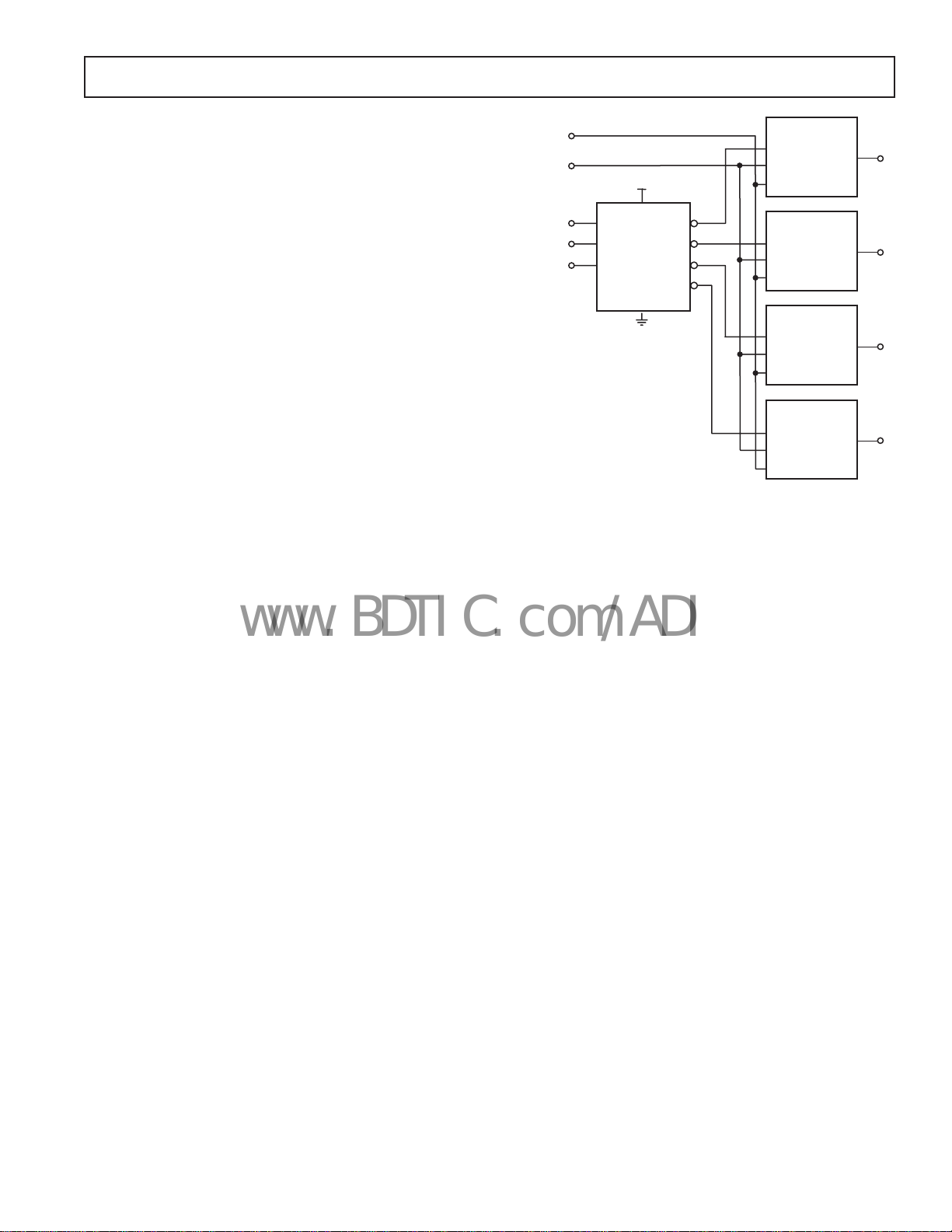
SYNC signal at any one time. The mux addressed will be deter-
ENABLE
DIN
SCLK
DGND
CODED
ADDRESS
DECODER
VDD
EN
DIN
SCLK
DIN
SCLK
DIN
SCLK
ADG725/
ADG731
SYNC
DIN
SCLK
SYNC
SYNC
SYNC
D
D
D
D
OTHER SPI
DEVICE
ADG725/
ADG731
OTHER SPI
DEVICE
www.BDTIC.com/ADI
mined by the decoder. There will be some digital feedthrough
from the digital input lines. Using a burst clock will minimize the
effects of digital feedthrough on the analog signal channels.
Figure 9 shows a typical circuit.
ADG725/ADG731
Figure 9. Addressing Multiple ADG725/ADG731s
Using a Decoder
REV. A
–15–

ADG725/ADG731
www.BDTIC.com/ADI
OUTLINE DIMENSIONS
48-Lead Lead Frame Chip Scale Package [LFCSP]
(CP-48)
Dimensions shown in millimeters
1.00
0.90
0.80
0.20
REF
12 MAX
SEATING
PLANE
BSC SQ
PIN 1
INDICATOR
VIEW
7.00
0.60 MAX
TOP
0.80 MAX
0.65 NOM
0.50 BSC
COMPLIANT TO JEDEC STANDARDS MO-220-VKKD-2
6.75
BSC SQ
COPLANARITY
0.50
0.40
0.30
0.05 MAX
0.02 NOM
0.08
37
36
25
24
0.60 MAX
48-Lead Thin Plastic Quad Flat Package [TQFP]
(SU-48)
Dimensions shown in millimeters
0.75
0.60
0.45
SEATING
PLANE
1.20
MAX
48
1
9.00
BSC SQ
TOP VIEW
(PINS DOWN)
37
36
BOTTOM
VIEW
5.50
REF
7.00
BSC SQ
0.30
0.23
0.18
PIN 1
48
INDICATOR
1
C02766–0–6/03(A)
5.25
SQ
5.10
4.95
12
13
COPLANARITY
0.08 MAX
0.15 MAX
0.05 MIN
COMPLIANT TO JEDEC STANDARDS MS-026ABC
0
MIN
1.05
1.00
0.95
7
0
12
13
Revision History
Location Page
6/03—Data Sheet changed from REV. 0 to REV. A.
Edits to ORDERING GUIDE . . . . . . . . . . . . . . . . . . . . . . . . . . . . . . . . . . . . . . . . . . . . . . . . . . . . . . . . . . . . . . . . . . . . . . . . . . . . . . 6
Edits to PIN CONFIGURATIONS . . . . . . . . . . . . . . . . . . . . . . . . . . . . . . . . . . . . . . . . . . . . . . . . . . . . . . . . . . . . . . . . . . . . . . . . . 7
Edits to PIN FUNCTION DESCRIPTIONS . . . . . . . . . . . . . . . . . . . . . . . . . . . . . . . . . . . . . . . . . . . . . . . . . . . . . . . . . . . . . . . . . . 7
Changes to Test Circuit 3 . . . . . . . . . . . . . . . . . . . . . . . . . . . . . . . . . . . . . . . . . . . . . . . . . . . . . . . . . . . . . . . . . . . . . . . . . . . . . . . . 11
Updated OUTLINE DIMENSIONS . . . . . . . . . . . . . . . . . . . . . . . . . . . . . . . . . . . . . . . . . . . . . . . . . . . . . . . . . . . . . . . . . . . . . . . 16
–16–
0.50
BSC
0.27
0.22
0.17
25
24
0.20
0.09
REV. A
 Loading...