Analog Devices ADG728 9 a Datasheet

CMOS, Low-Voltage, 2-Wire
S1
S8
SDADSCL
ADG728
S1A
DA
S4A
S1B
S4B
DB
ADG729
RESET
INPUT SHIFT
REGISTER
INPUT SHIFT
REGISTER
A0 A1 SDA SCL A0 A1
a
FEATURES
2-Wire Serial Interface
2.7 V to 5.5 V Single Supply
2.5 ⍀ On Resistance
0.75 ⍀ On-Resistance Flatness
100 pA Leakage Currents
Single 8-to-1 Matrix Switch ADG728
Dual 4-to-1 Matrix Switch ADG729
Power-On Reset
Small 16-Lead TSSOP Package
APPLICATIONS
Data Acquisition Systems
Communication Systems
Relay Replacement
Audio and Video Switching
Automatic Test Equipment
GENERAL DESCRIPTION
The ADG728 and ADG729 are CMOS analog matrix switches
with a serially controlled 2-wire interface. The ADG728 is an
8-channel matrix switch, while the ADG729 is a dual 4-channel
matrix switch. On resistance is closely matched between switches
and very flat over the full signal range. These parts can operate
equally well as either multiplexers, demultiplexers or switch
arrays and the input signal range extends to the supplies.
The ADG728 and ADG729 utilize a 2-wire serial interface that
is compatible with the I
external address pins (A0 and A1). This allows the 2 LSBs of
the 7-bit slave address to be set by the user. Four of each of the
devices can be connected to the one bus. The ADG728 also has
a RESET pin that should be tied high if not in use.
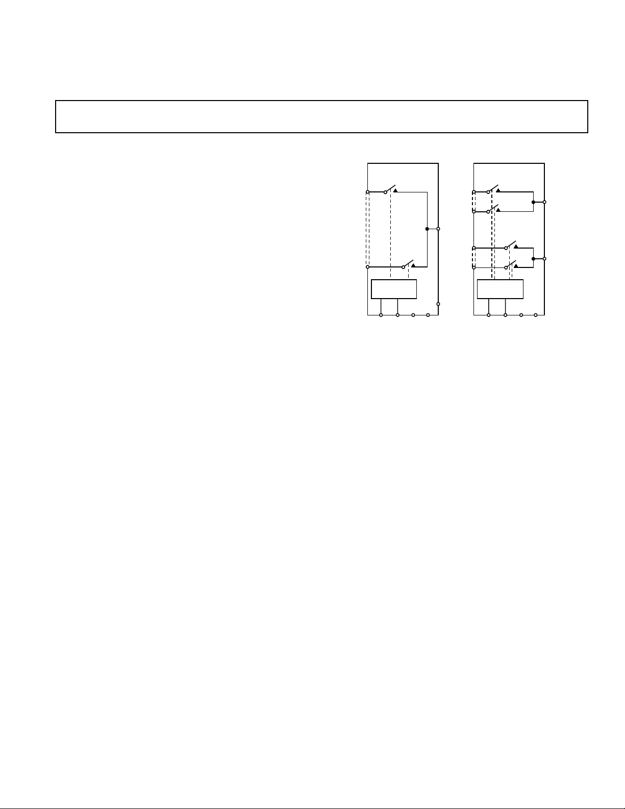
Each channel is controlled by one bit of an 8-bit word. This
means that these devices may be used in a number of different
configurations; all, any, or none of the channels may be on at
any one time.
On power-up of the device, all switches will be in the OFF condition and the internal shift register will contain all zeros.
All channels exhibit break-before-make switching action preventing momentary shorting when switching channels.
The ADG728 and ADG729 are available in 16-lead TSSOP
packages.
2
C™ interface standard. Both have two
Serially-Controlled, Matrix Switches
ADG728/ADG729
FUNCTIONAL BLOCK DIAGRAMS
PRODUCT HIGHLIGHTS
1. 2-Wire Serial Interface.
2. Single Supply Operation. The ADG728 and ADG729 are
fully specified and guaranteed with 3 V and 5 V supply rails.
3. Low On Resistance 2.5 Ω typical.
4. Any configuration of switches may be on at any one time.
5. Guaranteed Break-Before-Make Switching Action.
6. Small 16-Lead TSSOP Package.
I2C is a trademark of Philips Corporation.
REV. A
Information furnished by Analog Devices is believed to be accurate and
reliable. However, no responsibility is assumed by Analog Devices for its
use, nor for any infringements of patents or other rights of third parties
which may result from its use. No license is granted by implication or
otherwise under any patent or patent rights of Analog Devices.
One Technology Way, P.O. Box 9106, Norwood, MA 02062-9106, U.S.A.
Tel: 781/329-4700 World Wide Web Site: http://www.analog.com
Fax: 781/326-8703 © Analog Devices, Inc., 2000

ADG728/ADG729–SPECIFICATIONS
1
(VDD = 5 V ⴞ 10%, GND = 0 V, unless otherwise noted.)
B Version
–40ⴗC
Parameter 25ⴗC to +85ⴗC Unit Test Conditions/Comments
ANALOG SWITCH
Analog Signal Range 0 V to V
On Resistance (R
) 2.5 Ω typ VS = 0 V to VDD, IS = 10 mA;
ON
DD
V
4.5 5 Ω max Test Circuit 1
On-Resistance Match Between 0.4 Ω typ V
Channels (∆R
On-Resistance Flatness (R
) 0.8 Ω max
ON
) 0.75 Ω typ VS = 0 V to VDD, IS = 10 mA
FLAT(ON)
= 0 V to VDD, IS = 10 mA
S
1.2 Ω max
LEAKAGE CURRENTS V
Source OFF Leakage I
(OFF) ± 0.01 nA typ VD = 4.5 V/1 V, VS = 1 V/4.5 V, Test Circuit 2
S
= 5.5 V
DD
± 0.1 ± 0.3 nA max
Drain OFF Leakage I
(OFF) ± 0.01 nA typ VD = 4.5 V/1 V, VD = 1 V/4.5 V, Test Circuit 3
D
± 0.1 ± 1 nA max
Channel ON Leakage I
, IS (ON) ± 0.01 nA typ VD = VS = 4.5 V/1 V, Test Circuit 4
D
± 0.1 ± 1 nA max
INH
INL
2
2.4 V min
0.8 V max
LOGIC INPUTS (A0, A1)
Input High Voltage, V
Input Low Voltage, V
Input Current
I
INL
or I
INH
0.005 µA typ
± 0.1 µA max
CIN, Input Capacitance 6 pF typ
INH
INL
2
0.7 V
DD
V
+ 0.3 V max
DD
V min
–0.3 V min
0.3 V
DD
V max
DD
LOGIC INPUTS (SCL, SDA)
Input High Voltage, V
Input Low Voltage, V
, Input Leakage Current 0.005 µA typ VIN = 0 V to V
I
IN
± 1.0 µA max
, Input Hysteresis 0.05 V
V
HYST
DD
V min
CIN, Input Capacitance 6 pF typ
LOGIC OUTPUT (SDA)
VOL, Output Low Voltage 0.4 V max I
DYNAMIC CHARACTERISTICS
t
ON
t
OFF
2
= 3 mA
0.6 V max I
2
SINK
SINK
= 6 mA
95 ns typ RL = 300 Ω, CL = 35 pF, Test Circuit 5;
140 ns max V
= 3 V
S1
85 ns typ VS1 = 3 V, RL = 300 Ω, CL = 35 pF;
130 ns max Test Circuit 5
Break-Before-Make Time Delay, t
D
Charge Injection ±3 pC typ V
8 ns typ RL = 300 Ω, CL = 35 pF;
1ns minV
= VS2 = 3 V, Test Circuit 5
S1
= 2.5 V, RS = 0 Ω, CL = 1 nF;
S
Test Circuit 6
Off Isolation –55 dB typ R
–75 dB typ R
= 50 Ω, CL = 5 pF, f = 10 MHz;
L
= 50 Ω, CL = 5 pF, f = 1 MHz;
L
Test Circuit 8
Channel-to-Channel Crosstalk –55 dB typ R
–75 dB typ R
= 50 Ω, CL = 5 pF, f = 10 MHz;
L
= 50 Ω, CL = 5 pF, f = 1 MHz;
L
Test Circuit 7
–3 dB Bandwidth
ADG728 65 MHz typ R
= 50 Ω, CL = 5 pF, Test Circuit 8
L
ADG729 100 MHz typ
(OFF) 13 pF typ
C
S
C
(OFF)
D
ADG728 85 pF typ
ADG729 42 pF typ
, CS (ON)
C
D
ADG728 96 pF typ
ADG729 48 pF typ
POWER REQUIREMENTS V
I
DD
10 µA typ Digital Inputs = 0 V or 5.5 V
= 5.5 V
DD
20 µA max
N
OTES
1
Temperature range is as follows: B Version: –40°C to +85°C.
2
Guaranteed by design, not subject to production test.
Specifications subject to change without notice.
–2 – REV. A

ADG728/ADG729
1
SPECIFICATIONS
Parameter 25ⴗC to +85ⴗC Unit Test Conditions/Comments
ANALOG SWITCH
Analog Signal Range 0 V to V
On Resistance (R
On-Resistance Match Between 0.4 Ω typ V
Channels (∆R
On-Resistance Flatness (R
LEAKAGE CURRENTS V
Source OFF Leakage I
Drain OFF Leakage I
Channel ON Leakage I
LOGIC INPUTS (A0, A1)
Input High Voltage, V
Input Low Voltage, V
Input Current
I
or I
INL
INH
CIN, Input Capacitance 3 pF typ
LOGIC INPUTS (SCL, SDA)
Input High Voltage, V
Input Low Voltage, V
, Input Leakage Current 0.005 µA typ VIN = 0 V to V
I
IN
, Input Hysteresis 0.05 V
V
HYST
CIN, Input Capacitance 3 pF typ
LOGIC OUTPUT (SDA)
VOL, Output Low Voltage 0.4 V max I
DYNAMIC CHARACTERISTICS
t
ON
t
OFF
Break-Before-Make Time Delay, t
Charge Injection ±3 pC typ V
Off Isolation –55 dB typ R
Crosstalk –55 dB typ R
–3 dB Bandwidth
ADG728 65 MHz typ RL = 50 Ω, CL = 5 pF, Test Circuit 8
ADG729 100 MHz typ
(OFF) 13 pF typ
C
S
(OFF)
C
D
ADG728 85 pF typ
ADG729 42 pF typ
CD, CS (ON)
ADG728 96 pF typ
ADG729 48 pF typ
POWER REQUIREMENTS V
I
DD
NOTES
1
Temperature ranges are as follows: B Versions: –40°C to +85°C.
2
Guaranteed by design, not subject to production test.
Specifications subject to change without notice.
)6 Ω typ VS = 0 V to VDD, IS = 10 mA;
ON
) 1.2 Ω max
ON
FLAT(ON)
(OFF) ± 0.01 nA typ VS = 3 V/1 V, VD = 1 V/3 V, Test Circuit 2
S
(OFF) ± 0.01 nA typ VD = 3 V/1 V, VD = 1 V/3 V, Test Circuit 3
D
, IS (ON) ± 0.01 nA typ VD = VS = 3 V/1 V, Test Circuit 4
D
2
INH
INL
2
INH
INL
2
(VDD = 3 V ⴞ 10%, GND = 0 V, unless otherwise noted.)
B Version
11 12 Ω max Test Circuit 1
) 3.5 Ω typ VS = 0 V to VDD, IS = 10 mA
± 0.1 ±0.3 nA max
± 0.1 ±1 nA max
± 0.1 ±1 nA max
0.005 µA typ
DD
2
130 ns typ RL = 300 Ω, CL = 35 pF, Test Circuit 5;
115 ns typ RL = 300 Ω, CL = 35 pF;
D
8 ns typ RL = 300 Ω, CL = 35 pF;
–75 dB typ R
–75 dB typ R
10 µA typ Digital Inputs = 0 V or 3.3 V
–40ⴗC
DD
V
= 0 V to VDD, IS = 10 mA
S
= 3.3 V
DD
2.0 V min
0.4 V max
± 0.1 µA max
0.7 V
DD
V
+ 0.3 V max
DD
V min
–0.3 V min
0.3 V
DD
V max
DD
± 1.0 µA max
V min
= 3 mA
0.6 V max I
200 ns max V
180 ns max V
1ns minV
SINK
= 6 mA
SINK
= 2 V
S1
= 2 V, Test Circuit 5
S
= VS8 = 2 V, Test Circuit 5
S1
= 1.5 V, RS = 0 Ω, CL = 1 nF;
S
Test Circuit 6
= 50 Ω, CL = 5 pF, f = 10 MHz;
L
= 50 Ω, CL = 5 pF, f = 1 MHz;
L
Test Circuit 8
= 50 Ω, CL = 5 pF, f = 10 MHz;
L
= 50 Ω, CL = 5 pF, f = 1 MHz;
L
Test Circuit 7
= 3.3 V
DD
20 µA max
–3–REV. A

ADG728/ADG729
1
TIMING CHARACTERISTICS
(VDD = 2.7 V to 5.5 V. All specifications –40ⴗC to +85ⴗC, unless otherwise noted.)
Parameter Limit at T
f
SCL
t
1
t
2
t
3
t
4
t
5
t
6
2
400 kHz max SCL Clock Frequency
2.5 ms min SCL Cycle Time
0.6 ms min t
1.3 ms min t
0.6 ms min t
100 ns min t
0.9 ms max t
MIN
, T
MAX
Unit Conditions/Comments
, SCL High Time
HIGH
, SCL Low Time
LOW
, Start/Repeated Start Condition Hold Time
HD, STA
, Data Setup Time
SU, DAT
, Data Hold Time
HD, DAT
0ms min
t
7
t
8
t
9
0.6 ms min t
0.6 ms min t
1.3 ms min t
, Setup Time for Repeated Start
SU, STA
, Stop Condition Setup Time
SU, STO
, Bus Free Time Between a STOP Condition and
BUF
a Start Condition
t
10
t
11
C
b
4
t
SP
NOTES
1
See Figure 1.
2
A master device must provide a hold time of at least 300 ns for the SDA signal (referred to the VIH min of the SCL signal) in order to bridge the undefined region of
the falling edge of SCL.
3
Cb is the total capacitance of one bus line in pF. tR and tF measured between 0.3 VDD and 0.7 VDD.
4
Input filtering on both the SCL and SDA inputs suppress noise spikes which are less than 50 ns.
Specifications subject to change without notice.
300 ns max tR, Rise Time of Both SCL and SDA when Receiving
20 + 0.1C
3
b
ns min
250 ns max tF, Fall Time of SDA when Receiving
300 ns max t
3
0.1C
b
ns min
, Fall Time of SDA when Transmitting
F
400 pF max Capacitive Load for Each Bus Line
50 ns max Pulsewidth of Spike Suppressed
SDA
SCL
t
9
t
4
START
CONDITION
t
3
t
10
t
6
t
START
CONDITION
t
11
2
t
5
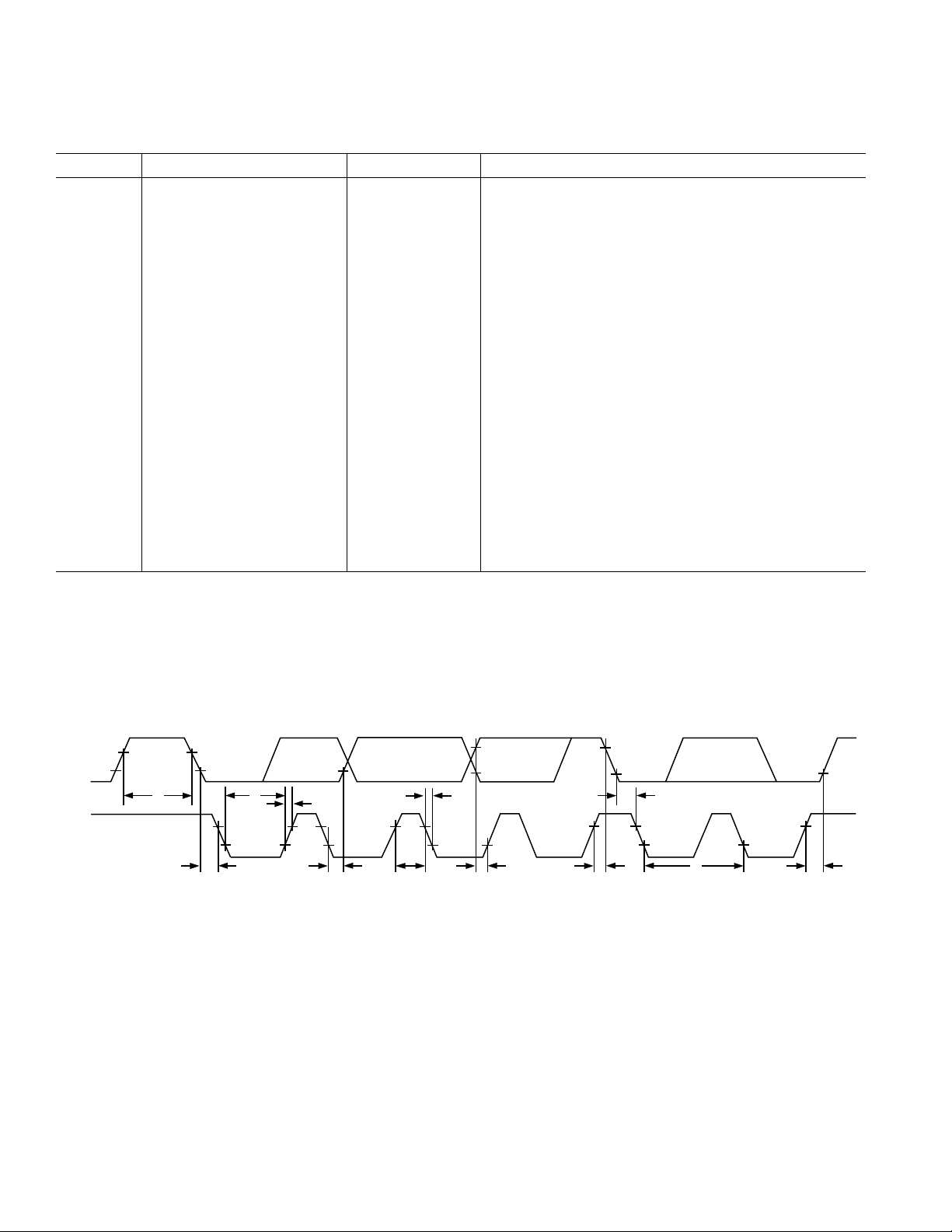
Figure 1. 2-Wire Serial Interface Timing Diagram
–4 – REV. A
t
7
REPEATED
START
CONDITION
t
4
t
1
t
8
STOP
CONDITION
 Loading...