

PRELIMINARY TECHNICAL DA T A
16-/32- Channel, Serially Controlled 4
=
1.8 V to 5.5 V, ±2.5 V, Analog Multiplexers
Preliminary Technical Data
FEATURES
3-Wire SPI Serial Interface
1.8 V to 5.5 V Single Supply
±2.5 V Dual Supply Operation
ΩΩ
4
Ω On Resistance
ΩΩ
ΩΩ
0.5
Ω On Resistance Flatness
ΩΩ
7mm x 7mm 48 lead Chip Scale Package (CSP)
or 48 lead TQFP package.
Rail to Rail Operation
Power On Reset
Fast Switching Times
Single 32 to 1 Channel Multiplexer
Dual/Differential 16 to 1 Channel Multiplexer
TTL/CMOS Compatible Inputs
For Functionally Equivalent devices with Parallel Interface
See ADG726/ADG732
APPLICATIONS
Optical Applications
Data Acquisition Systems
Communication Systems
Relay replacement
Audio and Video Switching
Battery Powered Systems
Medical Instrumentation
Automatic Test Equipment
S32
ΩΩ
Ω
ΩΩ
ADG725/ADG731
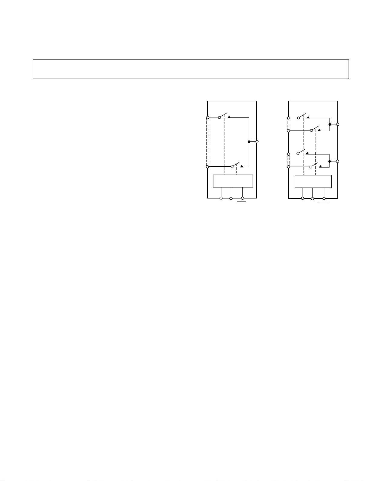
FUNCTIONAL BLOCK DIAGRAMS
ADG731
S1
INPUT SHIFT
REGISTER
SCLK
DIN
SYNC
S1A
S16A
D
S1B
S16B
ADG725
INPUT SHIFT
REGISTER
SCLK
DA
DB
DIN SYNC
GENERAL DESCRIPTION
The ADG725/ADG731 are monolithic CMOS 32
channel/dual 16 channel analog multiplexers with a
serially controlled 3-wire interface. The ADG732 switches
one of thirty-two inputs (S1-S32) to a common output, D.
The ADG725 can be configured as a dual mux switching
one of sixteen inputs to one output or a differential mux
switching one of sixteen inputs to a differential output.
These mulitplexers utilize a 3-wire serial interface that is
compatible with SPI
some DSP interface standards. On power-up, the internal
shift register contains all zeros and all switch are in the
OFF state.
These multiplexers are designed on an enhanced submicron process that provides low power dissipation yet gives
high switching speed, very low on resistance and leakage
currents. They operate from single supply of 1.8V to 5.5V
and ±2.5 V dual supply, making them ideally suited to a
variety of applications. On resistance is in the region of a
few Ohms and is closely matched between switches and
very flat over the full signal range. These parts can operate
equally well as either Multiplexers or De-Multiplexers
REV. PrD May 2002
Information furnished by Analog Devices is believed to be accurate and
reliable. However, no responsibility is assumed by Analog Devices for its
use, nor for any infringements of patents or other rights of third parties
which may result from its use. No license is granted by implication or
otherwise under any patent or patent rights of Analog Devices.
TM
, QSPITM, MICROWIRETM and
and have an input signal range which extends to the supplies. In the OFF condition, signal levels up to the
supplies are blocked. All channels exhibit break before
make switching action preventing momentary shorting
when switching channels.
They are available in either 48 lead CSP or TQFP
package.
PRODUCT HIGHLIGHTS
1. 3-Wire Serial Interface.
2. +1.8 V to +5.5 V Single or ±2.5 V Dual Supply
operation. These parts are specified and guaranteed
with +5 V ±10%, +3 V ±10% single supply and
±2.5 V ±10% dual supply rails.
3. On Resistance of 4 Ω.
4. Guaranteed Break-Before-Make Switching Action.
5. 7mm x 7mm 48 lead Chip Scale Package (CSP)
or 48 lead TQFP package.
One Technology Way, P.O. Box 9106, Norwood, MA 02062-9106, U.S.A.
Tel: 781/329-4700 www.analog.com
Fax: 781/326-8703 Analog Devices, Inc., 2002

PRELIMINARY TECHNICAL DA T A
1
ADG725/ADG731–SPECIFICATIONS
B Version
–40°C
Parameter +25oC to +85°C Units Test Conditions/Comments
ANALOG SWITCH
Analog Signal Range 0 V to V
On-Resistance (R
On-Resistance Match Between 0.3 Ω typ V
Channels (∆R
On-Resistance Flatness (R
LEAKAGE CURRENTS V
Source OFF Leakage I
Drain OFF Leakage I
ADG725 ±0.5 ±2.5 nA max Test Circuit 3
ADG731 ±1 ±5 nA max
Channel ON Leakage I
ADG725 ±0.5 ±2.5 nA max Test Circuit 4
ADG726 ±1 ±5 nA max
DIGITAL INPUTS
Input High Voltage, V
Input Low Voltage, V
Input Current
I
or I
INL
INH
CIN, Digital Input Capacitance 5 pF typ
DYNAMIC CHARACTERISTICS
t
TRANSITION
Break-Before-Make Time Delay, t
Charge Injection ±5 pC typ V
Off Isolation -60 dB typ R
Channel to Channel Crosstalk -60 dB typ R
-3 dB Bandwidth
ADG725 34 MHz typ R
ADG731 18 MHz typ
(OFF) 13 pF typ f = 1 MHz
C
S
C
(OFF)
D
ADG725 180 pF typ f = 1 MHz
ADG731 360 pF typ f = 1 MHz
, CS (ON)
C
D
ADG725 200 pF typ f = 1 MHz
ADG731 400 pF typ f = 1 MHz
POWER REQUIREMENTS V
I
DD
NOTES
1
Temperature range is as follows: B Version: –40°C to +85°C.
2
Guaranteed by design, not subject to production test.
Specifications subject to change without notice.
)4 Ω typ V
ON
5.5 6 Ω max Test Circuit 1
) 0.8 Ω max
ON
FLAT(ON)
) 0.5 Ω typ V
1 Ω max
(OFF) ±0.01 nA typ VD = 4.5 V/1 V, VS = 1 V/4.5 V;
S
±0.25 ±0.5 nA max Test Circuit 2
(OFF) ±0.05 nA typ VD = 4.5 V/1 V, VS = 1 V/4.5 V;
D
, IS (ON) ±0.05 nA typ VD = VS = 1 V, or 4.5V;
D
INH
INL
2.4 V min
0.8 V max
0.005 µA typ VIN = V
±0.1 µA max
2
40 ns typ R
60 ns max V
30 ns typ R
D
1 ns min V
10 µA typ Digital Inputs = 0 V or +5.5 V
20 µA max
(VDD = 5V ± 10%, VSS = 0V, GND = 0 V, unless otherwise noted)
V
DD
= 0 V to VDD, IDS = 10 mA;
S
= 0 V to V
S
= 0 V to VDD, IDS = 10 mA
S
= 5.5 V
DD
INL
= 300 Ω, C
L
= 3 V/0 V, V
S1
= 300 Ω, C
L
= 3 V, Test Circuit 6
S
= 0 V, R
S
, IDS = 10 mA
DD
or V
INH
= 35 pF,Test Circuit 5;
L
= 0 V/3V
S32
= 35 pF;
L
= 0 Ω, C
S
= 1 nF;
L
Test Circuit 7
= 50 Ω, C
L
= 5 pF, f = 100 kHz;
L
Test Circuit 8
= 50 Ω, C
L
= 5 pF, f = 100 kHz;
L
Test Circuit 9
= 50 Ω, C
L
= +5.5 V
DD
= 5 pF, Test Circuit 10
L
–2– REV. PrD

PRELIMINARY TECHNICAL DA T A
ADG725/ADG731
1
SPECIFICATIONS
Parameter +25oC to +85°C Units Test Conditions/Comments
ANALOG SWITCH
Analog Signal Range 0 V to V
On-Resistance (R
On-Resistance Match Between 0.4 Ω typ V
Channels (∆R
On-Resistance Flatness (R
LEAKAGE CURRENTS V
Source OFF Leakage I
Drain OFF Leakage I
ADG725 ±0.5 ±2.5 nA max Test Circuit 3
ADG731 ±1 ±5 nA max
Channel ON Leakage I
ADG725 ±0.5 ±2.5 nA max Test Circuit 4
ADG731 ±1 ±5 nA max
DIGITAL INPUTS
Input High Voltage, V
Input Low Voltage, V
Input Current
or I
I
INL
INH
CIN, Digital Input Capacitance 5 pF typ
DYNAMIC CHARACTERISTICS
t
TRANSITION
Break-Before-Make Time Delay, t
Charge Injection ±5 pC typ V
Off Isolation -60 dB typ R
Channel to Channel Crosstalk -60 dB typ R
-3 dB Bandwidth
ADG725 34 MHz typ R
ADG731 18 MHz typ
(OFF) 13 pF typ f = 1 MHz
C
S
C
(OFF)
D
ADG725 180 pF typ f = 1 MHz
ADG731 360 pF typ f = 1 MHz
, CS (ON)
C
D
ADG725 200 pF typ f = 1 MHz
ADG731 400 pF typ f = 1 MHz
POWER REQUIREMENTS V
I
DD
NOTES
1
Temperature ranges are as follows: B Version: –40°C to +85°C.
2
Guaranteed by design, not subject to production test.
Specifications subject to change without notice.
)7 Ω typ V
ON
)1Ω max
ON
D
D
INH
INL
(VDD = 3V ± 10%, VSS = 0V, GND = 0 V, unless otherwise noted)
B Version
–40°C
V
DD
= 0 V to VDD, IDS = 10 mA;
S
11 12 Ω max Test Circuit 1
= 0 V to V
S
FLAT(ON)
(OFF) ±0.01 nA typ VS = 3 V/1 V, VD = 1 V/3 V;
S
)3Ω max V
= 0 V to VDD, IDS = 10 mA
S
= 3.3 V
DD
, IDS = 10 mA
DD
±0.25 ±0.5 nA max Test Circuit 2
(OFF) ±0.05 nA typ VS = 1 V/3 V, VD = 3 V/1 V;
, IS (ON) ±0.05 nA typ VS = VD = +1 V or +3 V;
2.0 V min
0.8 V max
0.005 µA typ VIN = V
INL
or V
INH
±0.1 µA max
2
45 ns typ R
75 ns max V
30 ns typ R
D
1 ns min V
= 300 Ω, C
L
= 2 V/0 V, V
S1
= 300 Ω, C
L
= 2 V, Test Circuit 6
S
= 0 V, R
S
= 35 pF Test Circuit 5
L
= 0 V/2 V
S32
= 35 pF;
L
= 0 Ω, C
S
= 1 nF;
L
Test Circuit 7
= 50 Ω, C
L
= 5 pF, f = 1 MHz;
L
Test Circuit 8
= 50 Ω, C
L
= 5 pF, f = 1 MHz;
L
Test Circuit 9
= 50 Ω, C
L
= +3.3 V
DD
= 5 pF, Test Circuit 10
L
10 µA typ Digital Inputs = 0 V or +3.3 V
20 µA max
–3–REV. PrD

PRELIMINARY TECHNICAL DA T A
1
ADG725/ADG731–SPECIFICATIONS
(VDD = +2.5 V ±10%, VSS = -2.5 V ±10%, GND = 0 V, unless otherwise noted)
B Version
–40°C
Parameter +25oC to +85°C Units Test Conditions/Comments
ANALOG SWITCH
Analog Signal Range VSS to V
On-Resistance (R
On-Resistance Match Between 0.3 Ω typ V
Channels (∆R
On-Resistance Flatness (R
LEAKAGE CURRENTS V
Source OFF Leakage I
Drain OFF Leakage I
Channel ON Leakage I
DIGITAL INPUTS
Input High Voltage, V
Input Low Voltage, V
Input Current
I
or I
INL
INH
CIN, Digital Input Capacitance 5 pF typ
DYNAMIC CHARACTERISTICS
t
TRANSITION
Break-Before-Make Time Delay, t
Charge Injection ±8 pC typ V
Off Isolation -60 dB typ R
Channel to Channel Crosstalk -60 dB typ R
-3 dB Bandwidth
ADG725 34 MHz typ R
ADG731 18 MHz typ
C
(OFF) 13 pF typ
S
(OFF)
C
D
ADG725 180 pF typ f = 1 MHz
ADG731 360 pF typ f = 1 MHz
, CS (ON)
C
D
ADG725 200 pF typ f = 1 MHz
ADG731 400 pF typ f = 1 MHz
POWER REQUIREMENTS V
I
DD
I
SS
NOTES
1
Temperature range is as follows: B Version: –40°C to +85°C.
2
Guaranteed by design, not subject to production test.
Specifications subject to change without notice.
)4 Ω typ V
ON
5.5 6 Ω max Test Circuit 1
) 0.8 Ω max
ON
FLAT(ON)
) 0.5 Ω typ V
1 Ω max
(OFF) ±0.01 nA typ
S
±0.25 ±0.5 nA max Test Circuit 2
(OFF) ±0.05 nA typ
D
±0.5 ±2.5 nA max Test Circuit 3
±1 ±5 nA max
, IS (ON) ±0.01 nA typ
D
±0.5 ±2.5 nA max
±1 ±5 nA max
INH
INL
1.7 V min
0.7 V max
0.005 µA typ VIN = V
±0.1 µA max
2
40 ns typ R
60 ns max V
15 ns typ R
D
1 ns min V
10 µA typ Digital Inputs = 0 V or +2.75 V
20 µA max
10 µA typ VSS = -2.75 V
20 µA max Digital Inputs = 0 V or +2.75 V
Dual Supply
DD
V
= VSS to VDD, IDS = 10 mA;
S
= VSS to VDD, IDS = 10 mA
S
= VSS to VDD, IDS = 10 mA
S
= +2.75 V, VSS = -2.75 V
DD
VS = +2.25 V/-1.25 V, VD = -1.25 V/+2.25 V;
VS = +2.25 V/-1.25 V, VD = -1.25 V/+2.25 V;
VS = VD = +2.25 V/-1.25 V, Test Circuit 4
or V
INL
= 300 Ω, C
L
= 1.5 V/0 V,V
S1
= 300 Ω, C
L
= 1.5 V, Test Circuit 6
S
= 0 V, R
S
= 50 Ω, C
L
INH
= 35 pF Test Circuit 5
L
= 0 V/1.5 V
S32
= 35 pF;
L
= 0 Ω, C
S
= 5 pF, f = 1 MHz;
L
= 1 nF; Test 7
L
Test Circuit 8
= 50 Ω, C
L
= 5 pF, f = 1 MHz;
L
Test Circuit 9
= 50 Ω, C
L
= +2.75 V
DD
= 5 pF, Test Circuit 10
L
–4– REV. PrD

PRELIMINARY TECHNICAL DA T A
ADG725/ADG731
TIMING CHARACTERISTICS
1,2
Parameter Limit at T
t
1
t
2
t
3
t
4
t
5
t
6
t
7
t
8
NOTES
1
See Figure 1.
2
All input signals are specified with tr =tf = 5ns (10% to 90% of VDD) and timed from a voltage level of (VIL + VIH)/2.
Specifications subject to change without notice.
33 ns min SCLK Cycle time
13 ns min SCLK High Time
13 ns min SCLK Low Time
13 ns min SYNC to SCLK falling edge setup time
40 ns min Minimum SYNC low time
5 ns min Data Setup Time
4.5 ns min Data Hold Time
33 ns min Minimum SYNC high time
SCLK
SYNC
DIN
, T
MIN
MAX
t
8
t
4
t
5
t
7
t
6
DB7
Units Conditions/Comments
t
1
t
2
t
3
DB0
Figure 1. 3-Wire Serial Interface Timing Diagram.
DB7 (MSB)
EN CSA
CSB
A3 A2 A1 A0
X
DATA BITS
DB0 (LSB)
DB7 (MSB)
EN CS X
A4 A3 A2 A1 A0
DATA BITS
DB0 (LSB)
Figure 2. ADG725 Input Shift Register Contents Figure 3. ADG731 Input Shift Register Contents
–5–REV. PrD

ADG725/ADG731
PRELIMINARY TECHNICAL DA T A
ABSOLUTE MAXIMUM RATINGS
(TA = +25°C unless otherwise noted)
VDD to V
V
DD
V
SS
Analog Inputs
Digital Inputs
SS
to GND –0.3 V to +7 V
to GND +0.3 V to -7 V
2
2
30 mA, Whichever Occurs First
30 mA, Whichever Occurs First
Peak Current, S or D 60mA
(Pulsed at 1 ms, 10% Duty Cycle max)
Continuous Current, S or D 30mA
Operating Temperature Range
Industrial (B Version) –40°C to +85°C
1
+7 V
VSS - 0.3 V to VDD +0.3 Vor
-0.3V to VDD +0.3 V or
Storage Temperature Range –65°C to +150°C
Junction Temperature +150°C
48 lead CSP θ
48 lead TQFP θ
Thermal Impedance TBD°C/W
JA
Thermal Impedance TBD°C/W
JA
Lead Temperature, Soldering (10seconds) 300°C
IR Reflow, Peak Temperature +220°C
NOTES
1
Stresses above those listed under “Absolute Maximum Ratings” may cause permanent
damage to the device. This is a stress rating only and functional operation of the device
at these or any other conditions above those listed in the operational sections of this
specification is not implied. Exposure to absolute maximum rating conditions for
extended periods may affect device reliability. Only one absolute maximum rating may
be applied at any one time.
2
Overvoltages at SCLK, SYNC, DIN, RS, S or D will be clamped by internal diodes.
Current should be limited to the maximum ratings given.
CAUTION
ESD (electrostatic discharge) sensitive device. Electrostatic charges as high as 4000 V readily
accumulate on the human body and test equipment and can discharge without detection.
Although the ADG725/ADG731 features proprietary ESD protection circuitry, permanent damage
may occur on devices subjected to high energy electrostatic discharges. Therefore, proper ESD
precautions are recommended to avoid performance degradation or loss of functionality.
ORDERING GUIDE
Model Temperature Range Package Description Package Option
ADG725BCP -40
ADG725BSU -40
ADG731BCP -40
o
C to +85 oC Chip Scale Package (CSP) CP-48
o
C to +85 oC Thin Quad Flatpack SU-48
o
C to +85 oC Chip Scale Package (CSP) CP-48
ADG731BSU -40 oC to +85 oC Thin Quad Flatpack SU-48
–6– REV. PrD

PRELIMINARY TECHNICAL DA T A
PIN FUNCTION DESCRIPTION
ADG725 ADG731 Mnemonic Function
SCLK Serial Clock Input. Data is clocked into the input shift register on the falling edge of
the serial clock input. These devices can accomodate serial input rates of up to
30MHz.
RS Active low control input that clears the input register and turns all switches to the
OFF condition.
DIN Serial Data Input. Data is clocked into the 8-bit input register on the falling edge of
the serial clock input.
SXX Source. May be an input or output.
DX Drain. May be an input or output.
V
DD
GND Ground reference.
SYNC Active Low Control Input. This is the frame synchronization signal for the input
Power Supply Input. These parts can be operated from a supply of +1.8V to +5.5V
and dual supply of +/-2.5V.
data. When SYNC goes low, it powers on the SCLK and DIN buffers and the input
shift register is enabled. An 8-bit counter is also enabled. Data is transferred on the
falling edges of the following clocks. After 8 falling clock edges, switch conditions
are automaticaly updated. SYNC may be used to frame the signal, or just pulled low
for a short period of time to enable the counter and input buffers.
ADG725/ADG731
S12
S11
S10
S9
S8
S7
S6
S5
S4
S3
S2
S1
NC = NO CONNECT
S13
S14
S15
S16
(Not to Scale)
DDNCNC
NCDNCNCS32
ADG731
TOP VIEW
NCNCNC
DIN
SCLK
SYNC
48 47 46 45 44 39 38 3743 42 41 40
1
PIN 1
2
IDENTIFIER
3
4
5
6
7
8
9
10
11
12
13 14 15 16 17 18 19 20 21 22 23 24
VDDV
PIN CONFIGURATIONS
CSP & TQFP
S31
S30
S29
S12A
S11A
S10A
S9A
S8A
S7A
S6A
S5A
S4A
S3A
S2A
S1A
NC = NO CONNECT
GND
36
S28
35
S27
34
S26
33
S25
32
S24
31
S23
30
S22
29
S21
28
S20
27
S19
26
S18
25
S17
SS
V
S13A
S14A
S15A
PIN 1
IDENTIFIER
DDNCNC
VDDV
S16ANCDANCDB
ADG725
TOP VIEW
(Not to Scale)
DIN
SCLK
SYNC
NCNCNC
48 47 46 45 44 39 38 3743 42 41 40
1
2
3
4
5
6
7
8
9
10
11
12
13 14 15 16 17 18 19 20 21 22 23 24
S16A
S15B
S14B
GND
S13B
SS
V
36
S12B
35
S11B
34
S10B
33
S9B
32
S8B
31
S7B
30
S6B
29
S5B
28
S4B
27
S3B
26
S2B
25
S1B
–7–REV. PrD

PRELIMINARY TECHNICAL DA T A
ADG725/ADG731
Table 1. ADG725 Truth Table
A3 A2 A1 A0 EN CSA CSB Switch Condition
X X X X X 1 1 Retains previous switch condition
X X X X 1 1 1 All Switches OFF
0 0 0 0 0 0 0 S1A - DA, S1B - DB
0 0 0 1 0 0 0 S2A - DA, S2B - DB
0 0 1 0 0 0 0 S3A - DA, S3B - DB
0 0 1 1 0 0 0 S4A - DA, S4B - DB
0 1 0 0 0 0 0 S5A - DA, S5B - DB
0 1 0 1 0 0 0 S6A - DA, S6B - DB
0 1 1 0 0 0 0 S7A - DA, S7B - DB
0 1 1 1 0 0 0 S8A - DA, S8B - DB
1 0 0 0 0 0 0 S9A - DA, S9B - DB
1 0 0 1 0 0 0 S10A - DA, S10B - DB
1 0 1 0 0 0 0 S11A - DA, S11B - DB
1 0 1 1 0 0 0 S12A - DA, S12B - DB
1 1 0 0 0 0 0 S13A - DA, S13B - DB
1 1 0 1 0 0 0 S14A - DA, S14B - DB
1 1 1 0 0 0 0 S15A - DA, S15B - DB
1 1 1 1 0 0 0 S16A - DA, S16B - DB
Table 2. ADG731 Truth Table
A4 A3 A2 A1 A0 EN CS Switch Condition
X X XXXX1 Retains previous switch condition
X X X X X 1 1 All Switches OFF
0 0 000001
0 0 001002
0 0 010003
0 0 011004
0 0 100005
0 0 101006
0 0 110007
0 0 111008
0 1 000009
0 1 0010010
0 1 0100011
0 1 0110012
0 1 1000013
0 1 1010014
0 1 1100015
0 1 1110016
1 0 0000017
1 0 0010018
1 0 0100019
1 0 0110020
1 0 1000021
1 0 1010022
1 0 1100023
1 0 1110024
1 1 0000025
1 1 0010026
1 1 0100027
1 1 0110028
1 1 1000029
1 1 1010030
1 1 1100031
1 1 1110032
X = Don’t Care
–8– REV. PrD

PRELIMINARY TECHNICAL DA T A
ADG725/ADG731
TERMINOLOGY
V
DD
V
SS
I
DD
I
SS
GN D Ground (0 V) reference.
S Source terminal. May be an input or output.
D Drain terminal. May be an input or output.
IN Logic control input.
) Analog voltage on terminals D, S
V
D (VS
R
ON
∆R
ON
R
FLAT(ON)
I
(OFF) Source leakage current with the switch “OFF.”
S
I
(OFF) Drain leakage current with the switch “OFF.”
D
, IS (ON) Channel leakage current with the switch “ON.”
I
D
V
INL
V
INH
I
INL(IINH
(OFF) “OFF” switch source capacitance. Measured with reference to ground.
C
S
(OFF) “OFF” switch drain capacitance. Measured with reference to ground.
C
D
(ON) “ON” switch capacitance. Measured with reference to ground.
C
D,CS
C
IN
t
TRANSITION
t
OPEN
Charge A measure of the glitch impulse transferred from the digital input to the analog output during switching.
Injection
Off Isolation A measure of unwanted signal coupling through an “OFF” switch.
Crosstalk A measure of unwanted signal is coupled through from one channel to another as a result of parasitic
On Response The Frequency response of the “ON” switch.
Insertion The loss due to the ON resistance of the switch.
Loss
Most positive power supply potential.
Most Negative power supply in a dual supply application. In single supply applications, connect to GND.
Positive supply current.
Negative supply current.
Ohmic resistance between D and S.
On resistance match between any two channels, i.e. RONmax - RONmin
Flatness is defined as the difference between the maximum and minimum value of on-resistance as mea
sured over the specified analog signal range.
Maximum input voltage for logic “0”.
Minimum input voltage for logic “1”.
) Input current of the digital input.
Digital input capacitance.
Delay time measured between the 50% and 90% points of the SYNC and the switch “ON” condi
tion when switching from one address state to another.
“OFF” time measured between the 80% points of both switches when switching from one address state to
another.
capacitance.
–9–REV. PrD

PRELIMINARY TECHNICAL DA T A
ADG725/ADG731
TYPICAL PERFORMANCE CHARACTERISTICS
TBD
TPC 1. On Resistance vs. VD(VS) for for
Single Supply
TBD
TPC 2. On Resistance vs. VD(VS) for
Dual Supply
TBD
TPC 4. On Resistance vs. VD(VS) for
Different Temperatures, Single
Supply
TBD
TPC 5. On Resistance vs. VD(VS) for
Different Temperatures, Dual Supply
TBD
TPC 7. Leakage Currents vs. VD(VS)
TBD
TPC 8. Leakage Currents vs. VD(VS)
TBD
TPC 3. On Resistance vs. VD(VS) for
Different Temperatures, Single
Supply
TBD
TPC 6. Leakage Currents vs. VD(VS)
–10– REV. PrD
TBD
TPC 9. Leakage Currents vs.
Temperature

PRELIMINARY TECHNICAL DA T A
ADG725/ADG731
TBD
TPC 10. Leakage Currents vs.
Temperature
TBD
TPC 11. Supply Currents vs. Input
Switching Frequency
TBD
TPC 13. TON/T
Temperature
Times vs.
OFF
TBD
TPC 14. Off Isolation vs. Frequency
TBD
TPC 16. On Response vs. Frequency
TBD
TPC 12. Charge Injection vs. Source
Voltage
TBD
TPC 15. Crosstalk vs. Frequency
–11–REV. PrD

PRELIMINARY TECHNICAL DA T A
ADG725/ADG731
GENERAL DESCRIPTION
The ADG725 and ADG731 are serially controlled, 32
channel and dual/differential 16 channel multiplexers respectively.
POWER ON RESET
On power up of the device, all switches will be in the
OFF condition and the internal shift register is filled with
zeros and will remain so until a valid write takes place.
SERIAL INTERFACE
The ADG725 and ADG731 have a three wire serial interface (SYNC, SCLK, and DIN), which is compatible with
SPI, QSPI, MICROWIRE interface standards and most
DSP’s. Figure 1 shows the timing diagram of a typical
write sequence.
Data is written to the 8-bit shift register via DIN under
the control of the SYNC and SCLK signals.
When SYNC goes low, the input shift register is enabled.
An 8-bit counter is also enabled. Data from DIN is
clocked into the shift register on the falling edge of
SCLK. Figures 2 & 3 show the contents of the input shift
registers for these devices. When the part has received
eight clock cycles after SYNC has been pulled low, the
switches are automatically updated with the new
configuration and the input shift register is disabled. With
SYNC held high, any further data or noise on the DIN
line will have no effect on the shift register.
The ADG725 CSA and CSB data bits allow the user the
flexibility to change the configuration of either or both
banks of the multiplexer.
–12– REV. PrD

Test Circuits
D
Test Circuit 1. On Resistance.
IS(OFF)
V
S
PRELIMINARY TECHNICAL DA T A
ADG725/ADG731
I
DS
V
V
SS
DD
V1
S1
S
V
S
RON = V1/I
D
DS
S2
S32
V
S
Test Circuit 3. I
V
V
SS
DD
V
V
SS
DD
S1
S2
S32
V
D
GND
D
V
S
V
V
S1
S32
V
V
SS
DD
I
(OFF)
D
D
A
V
GND
(OFF)
D
V
DD
SS
V
DD
SS
GND
ID(ON)
D
A
V
D
Test Circuit 2. IS (OFF).
V
V
* SIMILAR CONNECTION FOR ADG725
*SIMILAR CONNECTION FOR ADG725
DD
DD
S2 THRU S31
ADG731*
GND
V
SS
V
SS
S1
S32
V
DD
V
DD
S2 THRU S3 1
ADG731*
GND
D
V
SS
V
SS
SYNC
V
S1
0V
V
R
300
S32
V
OUT
C
L
L
35pF
Ω
V
S1
V
OUT
V
S32
t
TRANSITION
Test Circuit 5. Switching Time of Multiplexer, t
SYNC
R
300
V
S
C
L
Ω
L
35pF
V
OUT
0V
V
S
V
OUT
80%
S1
S32
D
Test Circuit 4. I
50%
90%
TRANSITION
80%
t
OPEN
50%
t
.
(ON)
D
90%
TRANSITION
Test Circuit 6. Break Before Make Delay, t
OPEN
.
–13–REV. PrD

ADG725/ADG731
PRELIMINARY TECHNICAL DA T A
V
V
DD
SS
V
V
DD
SS
SYNC
R
S
V
S
V
V
DD
V
DD
ADG731*
GND
SS
V
SS
S
D
0.1µF
*SIMILAR CONNECTION FOR ADG725
S
GND
*SIMILAR CONNECTION FOR ADG725
0.1µF
50
Ω
OFF ISOLATION = 20 LOG
ADG731*
D
C
1nF
V
OUT
L
Test Circuit 7. Charge Injection.
NETWORK
ANALYZER
50
Ω
V
S
V
OUT
R
L
50
Ω
V
OUT
V
S
V
OUT
Q
= CL x ∆ V
INJ
V
V
DD
SS
S1
V
V
SS
DD
ADG731*
GND
*SIMILAR CONNECTION FOR ADG725
CH ANNEL TO CHANNEL CROSSTALK=
20LOG10(V
S2
S32
D
OUT/VS
50
Ω
)
OUT
∆
NETWORK
ANALYZER
50
Ω
V
OUT
R
L
50
Ω
V
OUT
V
S
Test Circuit 8. OFF Isolation
V
V
DD
V
DD
ADG731*
GND
SS
0.1µF
V
SS
S
D
INSERTION LOSS = 20 LOG VOUT WITH SWITCH
0.1µF
*SIMILAR CONNECTION FOR ADG725
Test Circuit 10. Bandwidth
NETWORK
ANALYZER
50
Ω
V
S
V
OUT
R
L
50
Ω
VOUT WITHOUT SWITCH
Test Circuit 9. Channel-to-Channel Crosstalk.
–14– REV. PrD
PRELIMINARY TECHNICAL DA T A
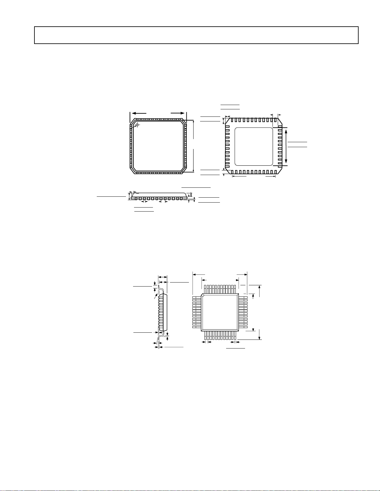
OUTLINE DIMENSIONS
Dimensions shown in inches and (mm).
48-Lead CSP
(CP-48)
0.024 (0.60)
PIN 1
INDICATOR
0.276(7.0)
BSC SQ
TOP
VIEW
0.024 (0.60)
0.017 (0.42)
0.009 (0.24)
0.266 (6.75)
BSC SQ
0.017 (0.42)
0.009 (0.24)
37 48
36
BOTTOM
VIEW
0.010 (0.25)
MIN
ADG725/ADG731
1
0.207 (5.25)
0.201 (5.10) SQ
0.195 (4.95)
0.035 (0.90) MAX
0.033 (0.85) NOM
0.020 (0.50)
0.016 (0.40)
0.012 (0.30)
o
MAX
12
0.012 (0.30)
0.009 (0.23)
0.007 (0.18)
0.020 (0.50)
BSC
0.028 (0.70) MAX
0.026 (0.65) NOM
0.002 (0.05)
0.008(0.20)
0.0004 (0.01)
REF
0.0 (0.0)
CONTROLLING DIMENSIONS ARE IN MILLIMETERS
48-Lead TQFP
(SU-48)
0.030 (0.75)
0.018 (0.45)
SEATING
PLANE
0.006 (0.15)
0.002 (0.05)
0° – 7
0.047 (1.20) MAX
0.041 (1.05)
0.037 (0.95)
°
0.008 (0.20)
0.004 (0.09)
0° MIN
0.354 (9.00) BSC
0.276 (7.0) BSC
48
1
12
13
0.019 (0.5)
BSC
TOP VIEW
(PINS DOWN)
25
24
37
24
0.011 (0.27)
0.006 (0.17)
36
25
0.217 (5.5)
REF
0.276 (7.0) BSC
0.354 (9.00) BSC
12
13
–15–REV. PrD
 Loading...