

Page 1
CMOS, Low Voltage, 4 Ω Dual SPST
www.BDTIC.com/ADI
FEATURES
1.8 V to 5.5 V single supply
4 Ω (max) on resistance
Low on resistance flatness
−3 dB bandwidth >200 MHz
Tiny package options
8-lead MSOP
3 mm × 2 mm LFCSP (A grade)
Fast switching times
t
, 20 ns
ON
t
, 10 ns
OFF
Low power consumption (<0.1 μW)
TTL/CMOS compatible
APPLICATIONS
USB 1.1 signal switching circuits
Cell phones
PDAs
Battery-powered systems
Communication systems
Sample hold systems
Audio signal routing
Video switching
Mechanical reed relay replacement
GENERAL DESCRIPTION
The ADG721, ADG722, and ADG723 are monolithic CMOS
SPST switches. These switches are designed on an advanced
submicron process that provides low power dissipation yet gives
high switching speed, low on resistance, and low leakage
currents. The devices are packaged in both a tiny 3 mm × 2 mm
LFCSP and an MSOP, making them ideal for space-constrained
applications.
The ADG721, ADG722, and ADG723 are designed to operate
rom a single 1.8 V to 5.5 V supply, making them ideal for use
f
in battery-powered instruments and with the new generation of
DACs and ADCs from Analog Devices, Inc.
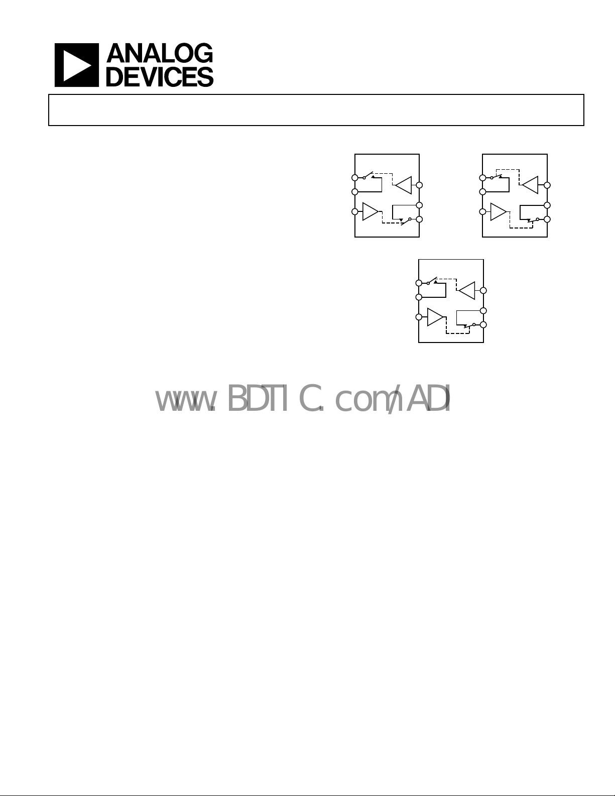
The ADG721, ADG722, and ADG723 contain two independent
sin
gle-pole/single-throw (SPST) switches. The ADG721 and
ADG722 differ only in that both switches are normally open
Switches in 3 mm × 2 mm LFCSP
ADG721/ADG722/ADG723
FUNCTIONAL BLOCK DIAGRAMS
S1
D1
IN2
ADG722
IN1
D2
S2
00045-003
IN1
D2
S2
00045-002
ADG721
S1
D1
IN2
Figure 1. Figure 2.
IN1
D2
S2
00045-001
ADG723
S1
D1
IN2
SWITCHES SHOWN FOR
A LOGIC "0" INPUT
Figure 3.
and normally closed, respectively. In the ADG723, Switch 1 is
normally open and Switch 2 is normally closed.
Each switch of the ADG721, ADG722, and ADG723 conducts
ually well in both directions when on. The ADG723 exhibits
eq
break-before-make switching action.
PRODUCT HIGHLIGHTS
1. 1.8 V to 5.5 V single-supply operation.
r y low R
2. Ve
3. L
ow on resistance flatness.
4. −3 dB ban
5. L
ow power dissipation. CMOS construction ensures low
power dissipation.
6. 8-lead MSO
(4 Ω max at 5 V, 10 Ω max at 3 V).
ON
dwidth >200 MHz.
P and 3 mm × 2 mm LFCSP.
Rev. B
Information furnished by Analog Devices is believed to be accurate and reliable. However, no
responsibility is assumed by Anal og Devices for its use, nor for any infringements of patents or ot her
rights of third parties that may result from its use. Specifications subject to change without notice. No
license is granted by implication or otherwise under any patent or patent rights of Analog Devices.
Trademarks and registered trademarks are the property of their respective owners.
One Technology Way, P.O. Box 9106, Norwood, MA 02062-9106, U.S.A.
Tel: 781.329.4700 www.analog.com
Fax: 781.461.3113 ©2004–2007 Analog Devices, Inc. All rights reserved.
Page 2

ADG721/ADG722/ADG723
www.BDTIC.com/ADI
TABLE OF CONTENTS
Features.............................................................................................. 1
Terminology.......................................................................................7
Applications....................................................................................... 1
Functional Block Diagrams............................................................. 1
General Description ......................................................................... 1
Product Highlights ........................................................................... 1
Revision History ............................................................................... 2
Specifications..................................................................................... 3
Absolute Maximum Ratings............................................................ 5
ESD Caution.................................................................................. 5
Pin Configuration and Pin Descriptions....................................... 6
REVISION HISTORY
2/07—Rev. A to Rev. B
Updated Format..................................................................Universal
Changes to Specifications................................................................ 3
Changes to Absolute Maximum Ratings....................................... 5
Change to Figure 4 ........................................................................... 6
Updated Outline Dimensions....................................................... 13
Changes to Ordering Guide.......................................................... 13
3/04—Rev. 0 to Rev. A
Additions to Applications................................................................ 1
Changes to Ordering Guide............................................................ 4
Updated Outline Dimensions....................................................... 10
Typical Performance Characteristics..............................................8
Test Circuits..................................................................................... 10
Applications..................................................................................... 12
ADG721/ADG722/ADG723 Supply Voltages ....................... 12
On Response vs. Frequency ...................................................... 12
Off Isolation ................................................................................ 12
Outline Dimensions....................................................................... 13
Ordering Guide .......................................................................... 14
Rev. B | Page 2 of 16
Page 3
ADG721/ADG722/ADG723
www.BDTIC.com/ADI
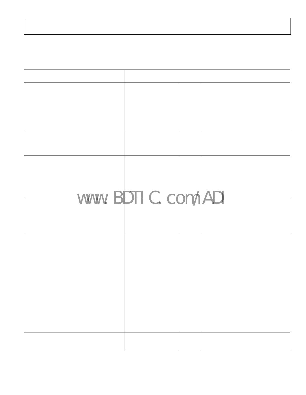
SPECIFICATIONS
VDD = 5 V ± 10%, GND = 0 V. All specifications −40°C to +85°C, unless otherwise noted.
Table 1.
A, B Grade
1
Parameter +25°C −40°C to +85°C Unit Test Conditions/Comments
ANALOG SWITCH
Analog Signal Range 0 to VDD V
On Resistance, RON 2.5 Ω typ VS = 0 V to VDD, IS = −10 mA
4 5 Ω max See Figure 12
On Resistance Match Between Channels, ∆RON 0.3 Ω typ VS = 0 V to VDD, IS = −10 mA
1.0 Ω max
On Resistance Flatness, R
0.85 Ω typ VS = 0 V to VDD, IS = −10 mA
FLAT(ON)
1.5 Ω max
LEAKAGE CURRENTS – A Grade VDD = 5.5 V
Source off Leakage, IS (OFF) ±0.01 nA typ VS = 4.5 V/1 V, VD = 1 V/4.5 V, see Figure 13
Drain off Leakage, ID (OFF) ±0.01 nA typ VS = 4.5 V/1 V, VD = 1 V/4.5 V, see Figure 13
Channel on Leakage, ID, IS (ON) ±0.01 nA typ VS = VD = 1 V or VS = VD = 4.5 V, see Figure 14
LEAKAGE CURRENTS – B Grade VDD = 5.5 V
Source off Leakage, IS (OFF) ±0.01 nA typ VS = 4.5 V/1 V, VD = 1 V/4.5 V
±0.25 ±0.35 nA max Test Circuit 2
Drain off Leakage, ID (OFF) ±0.01 nA typ VS = 4.5 V/1 V, VD = 1 V/4.5 V
±0.25 ±0.35 nA max See Figure 13
Channel on Leakage, ID, IS (ON) ±0.01 nA typ VS = VD = 1 V or VS = VD = 4.5 V
±0.25 ±0.35 nA max See Figure 14
DIGITAL INPUTS
Input High Voltage, V
Input Low Voltage, V
2.4 V min
INH
0.8 V max
INL
Input Current
I
or I
0.005 μA typ VIN = V
INL
INH
INL
or V
INH
±0.1 μA max
DYNAMIC CHARACTERISTICS2
tON 14 ns typ RL = 300 Ω, CL = 35 pF
20 ns max VS = 3 V, see Figure 15
t
6 ns typ RL = 300 Ω, CL = 35 pF
OFF
10 ns max VS = 3 V, see Figure 15
Break-Before-Make Time Delay, tD (ADG723 Only) 7 ns typ RL = 300 Ω, CL = 35 pF
1 ns min VS1 = VS2 = 3 V, see Figure 16
Charge Injection 2 pC typ VS = 2 V, RS = 0 Ω, CL = 1 nF, see Figure 17
Off Isolation −60 dB typ RL = 50 Ω, CL = 5 pF, f = 10 MHz
−80 dB typ RL = 50 Ω, CL = 5 pF, f = 1 MHz, see Figure 18
Channel-to-Channel Crosstalk −77 dB typ RL = 50 Ω, CL = 5 pF, f = 10 MHz
−97 dB typ RL = 50 Ω, CL = 5 pF, f = 1 MHz, see Figure 19
Bandwidth −3 dB 200 MHz typ RL = 50 Ω, CL = 5 pF, see Figure 20
CS (OFF) 7 pF typ
CD (OFF) 7 pF typ
CD, CS (ON) 18 pF typ
POWER REQUIREMENTS VDD = 5.5 V
IDD 0.001 μA typ Digital inputs = 0 V or 5 V
1.0 μA max
1
Temperature range: A, B grades, −40°C to +85°C. All specifications apply to both grades unless otherwise stated.
2
Guaranteed by design; not subject to production test.
Rev. B | Page 3 of 16
Page 4
ADG721/ADG722/ADG723
www.BDTIC.com/ADI
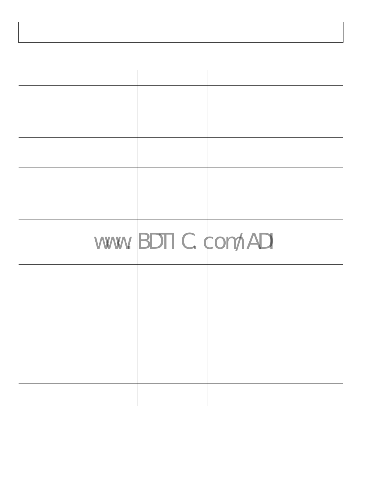
VDD = 3 V ± 10%, GND = 0 V. All specifications −40°C to +85°C, unless otherwise noted.
Table 2.
A, B Grades
1
Parameter +25°C −40°C to +85°C Unit Test Conditions/Comments
ANALOG SWITCH
Analog Signal Range 0 to VDD V
On Resistance, RON 6.5 Ω typ VS = 0 V to VDD, IS = −10 mA
10 Ω max See Figure 12
On Resistance Match Between Channels, ∆RON 0.3 Ω typ VS = 0 V to VDD, IS = −10 mA
1.0 Ω max
On Resistance Flatness, R
3.5 Ω typ VS = 0 V to VDD, IS = −10 mA
FLAT(ON)
LEAKAGE CURRENTS – A Grade VDD = 3.3 V
Source off Leakage, IS (OFF) ±0.01 nA typ VS = 3 V/1 V, VD = 1 V/3 V, see Figure 13
Drain off Leakage, ID (OFF) ±0.01 nA typ VS = 3 V/1 V, VD = 1 V/3 V, see Figure 13
Channel on Leakage, ID, IS (ON) ±0.01 nA typ VS = VD = 1 V or 3 V, Figure 14
LEAKAGE CURRENTS – B Grade VDD = 3.3 V
Source off Leakage, IS (OFF) ±0.01 nA typ VS = 3 V/1 V, VD = 1 V/3 V
±0.25 ±0.35 nA max See Figure 13
Drain off Leakage, ID (OFF) ±0.01 nA typ VS = 3 V/1 V, VD = 1 V/3 V
±0.25 ±0.35 nA max See Figure 13
Channel on Leakage, ID, IS (ON) ±0.01 nA typ VS = VD = 1 V or 3 V
±0.25 ±0.35 nA max See Figure 14
DIGITAL INPUTS
Input High Voltage, V
Input Low Voltage, V
2.0 V min
INH
0.4 V max
INL
Input Current
I
or I
0.005 μA typ VIN = V
INL
INH
INL
or V
INH
±0.1 μA max
DYNAMIC CHARACTERISTICS2
tON 16 ns typ RL = 300 Ω, CL = 35 pF
24 ns max VS = 2 V, see Figure 15
t
7 ns typ RL = 300 Ω, CL = 35 pF
OFF
11 ns max VS = 2 V, see Figure 15
Break-Before-Make Time Delay, tD (ADG723 Only) 7 ns typ RL = 300 Ω, CL = 35 pF
1 ns min VS1 = VS2 = 2 V, see Figure 16
Charge Injection 2 pC typ VS = 1.5 V, RS = 0 Ω, CL = 1 nF, see Figure 17
Off Isolation −60 dB typ RL = 50 Ω, CL = 5 pF, f = 10 MHz
−80 dB typ RL = 50 Ω, CL = 5 pF, f = 1 MHz, see Figure 18
Channel-to-Channel Crosstalk −77 dB typ RL = 50 Ω, CL = 5 pF, f = 10 MHz
−97 dB typ RL = 50 Ω, CL = 5 pF, f = 1 MHz, see Figure 19
Bandwidth −3 dB 200 MHz typ RL = 50 Ω, CL = 5 pF, see Figure 20
CS (OFF) 7 pF typ
CD (OFF) 7 pF typ
CD, CS (ON) 18 pF typ
POWER REQUIREMENTS VDD = 3.3 V
IDD 0.001 μA typ Digital inputs = 0 V or 3 V
1.0 μA max
1
Temperature range: A, B Grades, −40°C to +85°C. All specifications apply to both grades unless otherwise stated.
2
Guaranteed by design; not subject to production test.
Rev. B | Page 4 of 16
Page 5
ADG721/ADG722/ADG723
www.BDTIC.com/ADI
ABSOLUTE MAXIMUM RATINGS
TA = 25°C unless otherwise noted.
Table 3.
Parameter Rating
VDD to GND −0.3 V to +7 V
Analog, Digital Inputs1
Continuous Current, S or D 30 mA
Operating Temperature Range
Industrial (A, B Grade) −40°C to +85°C
Storage Temperature Range −65°C to +150°C
Junction Temperature +150°C
8-Lead MSOP
θJA Thermal Impedance 206°C/W
θJC Thermal Impedance 44°C/W
8-Lead LFCSP (4-Layer Board)
θJA Thermal Impedance1 50.8°C/W
Lead Temperature, Soldering
Vapor Phase (60 sec) 215°C
Infrared (15 sec) 220°C
Lead-Free Temperature,
Soldering
IR Reflow, Peak Temperature 260°C (+0/−5°C)
Time at Peak Temperature 10 sec to 40 sec
ESD 2 kV
1
Assumes exposed paddle is tied to ground.
−0.3 V to V
whichever occurs first
+ 0.3 V or 30 mA,
DD
Stresses above those listed under Absolute Maximum Ratings
may cause permanent damage to the device. This is a stress
rating only; functional operation of the device at these or any
other conditions above those indicated in the operational
section of this specification is not implied. Exposure to absolute
maximum rating conditions for extended periods may affect
device reliability.
ESD CAUTION
Rev. B | Page 5 of 16
Page 6

ADG721/ADG722/ADG723
www.BDTIC.com/ADI
PIN CONFIGURATION AND PIN DESCRIPTIONS
V
1
S1
ADG721/
ADG722/
2
D1
ADG723
3
IN2
TOP VIEW
(Not to Scale)
GND
4
NOTES
1. EXPOSED PADDLE OF LFCSP
SHOULD BE TIED TO GROUND.
Figure 4. Pin Configuration
Table 4. Pin Function Descriptions
Pin No. Mnemonic Descriptions
1 S1 Source Pin 1. May be an input or an output.
2 D1 Drain Pin 1. May be an input or an output.
3 IN2
Logic Control Input for Switch S1ÆD1.
4 GND Ground (0 V) Reference.
5 S2 Source Pin 2. May be an input or an output.
6 D2 Drain Pin 2. May be an input or an output.
7 IN1
Logic Control Input for Switch S2ÆD2.
8 VDD Positive Power Supply Input.
8
DD
7
IN1
6
D2
5
S2
00045-004
Table 5. Truth Table (ADG721/ADG722)
ADG721 In ADG722 In Switch Condition
0 1 Off
1 0 On
Table 6. Truth Table (ADG723)
Logic Switch 1 Switch 2
0 Off On
1 On Off
Rev. B | Page 6 of 16
Page 7

ADG721/ADG722/ADG723
www.BDTIC.com/ADI
TERMINOLOGY
VDD
Most positive power supply potential.
V
(VS)
D
Analog voltage on the D and S terminals.
GND
Ground (0 V) reference.
S
Source terminal. May be an input or output.
D
Drain terminal. May be an input or output.
IN
Logic control input.
R
ON
Ohmic resistance between D and S.
ΔR
ON
On resistance match between any two channels, that is,
max − RON min.
R
ON
R
FLAT(ON)
Flatness is defined as the difference between the maximum and
minimum value of on resistance as measured over the specified
analog signal range.
I
(OFF)
S
Source leakage current with the switch off.
I
(OFF)
D
Drain leakage current with the switch off.
I
, IS (ON)
D
Channel leakage current with the switch on.
C
(OFF)
S
Off switch source capacitance.
(OFF)
C
D
Off switch drain capacitance.
C
, CS (ON)
D
On switch capacitance.
t
ON
Delay between applying the digital control input and the output
tching on.
swi
t
OFF
Delay between applying the digital control input and the output
swi
tching off.
t
D
Off time or on time measured between the 90% points of both
tches, when switching from one address state to another
swi
(ADG723 only).
Crosstalk
A measure of unwanted signal that is the result of parasitic
ca
pacitance.
Off Isolation
A measure of unwanted signal coupling through an off switch.
Charge Injection
A measure of the glitch impulse transferred during switching.
Rev. B | Page 7 of 16
Page 8

ADG721/ADG722/ADG723
–
–
www.BDTIC.com/ADI
TYPICAL PERFORMANCE CHARACTERISTICS
6.0
5.5
5.0
4.5
4.0
3.5
(Ω)
3.0
ON
R
2.5
2.0
1.5
1.0
0.5
0
0 0.5 1.0 1.5 2.0 2.5 3.0 3.5 4.0 4.5 5.0
V
= 3.0V
DD
VD OR VS – DRAIN OR SOURCE VO LTAGE (V)
= 2.7V
V
DD
V
DD
V
DD
Figure 5. On Resistance as a Function of V
6
5
4
(Ω)
3
ON
R
2
+85°C
+25°C
–40°C
T
= 4.5V
= 5.0V
(VS), Single Supplies
D
= 25°C
A
V
DD
= 3V
00045-005
1m
V
= 5V
DD
100µ
10µ
(A)
1µ
SUPPLY
I
100n
10n
1n
10 100 1k 10k 100k 1M 10M
FREQUENCY (Hz)
Figure 8. Supply Current vs. Input Switching Frequency
30
VDD = 3V, 5V
–40
–50
–60
–70
OFF ISOLATION (dB)
–80
0045-008
1
0
0 0.5 1.0 1.5 2.0 2.5 3.0
VD OR VS – DRAIN OR SOURCE VO LTAGE (V)
Figure 6. On Resistance as a Function of a V
= 3 V
V
DD
6.0
5.5
5.0
4.5
4.0
3.5
(Ω)
3.0
ON
R
2.5
2.0
1.5
1.0
0.5
0
0 0.5 1.0 1.5 2.0 2.5 3.0 3.5 4.0 4.5 5.0
VD OR VS – DRAIN OR SOURCE VOLTAGE (V)
+85°C+25°C
–40°C
Figure 7. On Resistance as a Function of V
= 5 V
V
DD
(VS) for Different Temperatures,
D
VDD = 5V
(VS) for Different Temperatures,
D
–90
–100
10k 100k 1M 10M 100M
00045-006
Figure 9. Off Isolat
30
VDD = 3V, 5V
–40
–50
–60
–70
–80
CROSSTALK (d B)
–90
–100
–110
10k 100k 1M 10M 100M
00045-007
FREQUENCY (Hz)
ion vs. Frequency
FREQUENCY (Hz)
00045-009
00045-010
Figure 10. Crosstalk vs. Frequency
Rev. B | Page 8 of 16
Page 9

ADG721/ADG722/ADG723
–
www.BDTIC.com/ADI
6
V
= 5V
DD
–7
–8
–9
–10
ON RESPONSE (dB)
–11
–12
Figure 11. On Response vs. Frequency
10k 100k 1M 10M 100M
1k100
FREQUENCY (Hz)
00045-011
Rev. B | Page 9 of 16
Page 10

ADG721/ADG722/ADG723
V
V
V
VDDV
V
V
www.BDTIC.com/ADI
TEST CIRCUITS
I
DS
V1
SD
V
S
R
ON
Figure 12. On Resistance
= V1/I
IS (OFF) ID(OFF)
DS
0045-012
DD
0.1µF
V
DD
SD
V
S
IN
GND
S
R
300Ω
SD
A A
Figure 13. Off Leakage
V
IN
V
OUT
C
L
L
35pF
V
IN
V
OUT
V
D
ADG721
ADG722
00045-013
50% 50%
50% 50%
90%
t
ON
SD
S
Figure 14. On Leakage
90%
t
OFF
00045-015
Figure 15. Switching Times
ID(ON)
A
V
D
00045-014
0.1µF
V
V
S1
S2
S1 D1
S2
IN1, IN2
V
IN
DD
GND
V
OUT1
C
R
L1
V
C
L2
35pF
OUT2
300Ω
D2
R
L2
300Ω
L1
35pF
Figure 16. Break-Before-Make Time Delay, t
DD
V
R
S
V
S
IN
DD
SD
GND
C
1nF
L
V
OUT
IN
V
OUT
V
IN
0V
V
OUT1
0V
V
OUT2
0V
(ADG723 Only)
D
SW ON SW OFF
90%
Q
INJ
= CL × ΔV
50% 50%
90%
t
D
ΔV
OUT
OUT
t
90%
D
90%
00045-016
00045-017
Figure 17. Charge Injection
Rev. B | Page 10 of 16
Page 11

ADG721/ADG722/ADG723
V
V
V
V
V
www.BDTIC.com/ADI
DD
0.1µF
DD
0.1µF
V
DD
SD
IN
V
S
IN
GND
Figure 18. Off Isolation
V
NC
V
OUT
R
L
50Ω
S
V
IN
00045-018
Figure 19. Channel-to-Channel Crosstalk
DD
0.1µF
V
DD
SD
V
S
IN1
SD
GND
CHANNEL-TO-CHANNEL
CROSSTALK
|
= 20 × log
VS/V
V
OUT
50Ω
IN2
V
OUT
R
L
50Ω
|
V
DD
SD
IN
GND
00045-020
R
50Ω
V
OUT
L
00045-019
Figure 20. Bandwidth
Rev. B | Page 11 of 16
Page 12

ADG721/ADG722/ADG723
V
(
www.BDTIC.com/ADI
APPLICATIONS
The ADG721/ADG722/ADG723 belong to a new family of
Analog Devices CMOS switches. This series of general-purpose
switches has improved switching times, lower on resistance, higher
bandwidths, low power consumption, and low leakage currents.
ADG721/ADG722/ADG723 SUPPLY VOLTAGES
Functionality of the ADG721/ADG722/ADG723 extends from
a 1.8 V to a 5.5 V single supply, which makes it ideal for batterypowered instruments, where important design parameters are
power efficiency and performance.
It is important to note that the supply voltage affects the input
sig
nal range, the on resistance, and the switching times of the part.
The typical performance characteristics and the specifications
clearly show the effects of the power supplies.
= 1.8 V, on resistance is typically 40 Ω over the
For V
DD
temperature range.
ON RESPONSE VS. FREQUENCY
Figure 21 illustrates the parasitic components that affect the ac
performance of CMOS switches (the switch is shown surrounded
by a box). Additional external capacitances further degrade some
aspects of performance. These capacitances affect feedthrough,
crosstalk, and system bandwidth.
C
DS
S
R
ON
IN
Figure 21. Switch Represented by Equiva
C
The transfer function that describes the equivalent diagram of
the switch (Figure 21) is of the form (A)s, as shown in the
lowing equation:
fol
⎡
()
CRs
ON
DSON
RCRs
=
)(
RsA
⎢
T
()
⎢
⎣
D
D
+
1
+
TT
C
LOAD
lent Parasitic Components
⎤
⎥
1
⎥
⎦
R
LOAD
V
OUT
00045-021
The signal transfer characteristic is dependent on the switch
channel capacitance, C
. This capacitance creates a frequency
DS
zero in the numerator of the transfer function A(s). Because the
switch on resistance is small, this zero usually occurs at high
frequencies. The bandwidth is a function of the switch output
capacitance combined with C
and the load capacitance. The
DS
frequency pole corresponding to these capacitances appears in
the denominator of A(s).
The dominant effect of the output capacitance, C
, causes the
D
pole breakpoint frequency to occur first. Therefore, in order to
maximize bandwidth, a switch must have a low input and
output capacitance and low on resistance (see
Figure 11).
OFF ISOLATION
Off isolation is a measure of the input signal coupled through
R
LOAD
, couples
DS
V
OUT
00045-022
an off switch to the switch output. The capacitance, C
the input signal to the output load, when the switch is off, as
shown in Figure 22.
C
DS
S
V
IN
Figure 22. Off Isolation Is Affected by External Load
C
Resi
stance and Capacitance
D
D
C
LOAD
The larger the value of CDS, the larger the value of feedthrough
produced. Figure 9 illustrates the drop in off isolation as a
unction of frequency. From dc to roughly 1 MHz, the switch
f
shows better than −80 dB isolation. Up to frequencies of 10
MHz, the off isolation remains better than −60 dB. As the
frequency increases, more and more of the input signal is
coupled through to the output. Off isolation can be maximized
by choosing a switch with the smallest C
possible. The values
DS
of load resistance and capacitance also affect off isolation
because they contribute to the coefficients of the poles and
zeros in the transfer function of the switch when open.
where:
CT = C
= R
R
T
+ CD + CDS
LOAD
/(R
LOAD
LOAD
+ RON)
Rev. B | Page 12 of 16
⎡
=1)(
sA
⎢
()
⎢
⎣
)
CRs
DSLOAD
()
LOADLOAD
CCCRs
D
⎤
⎥
+++
⎥
DS
⎦
Page 13

ADG721/ADG722/ADG723
www.BDTIC.com/ADI
OUTLINE DIMENSIONS
3.20
3.00
2.80
8
5
3.20
3.00
2.80
PIN 1
0.95
0.85
0.75
0.15
0.00
COPLANARITY
1
0.65 BSC
0.38
0.22
0.10
5.15
4.90
4.65
4
SEATING
PLANE
1.10 MAX
0.23
0.08
8°
0°
0.80
0.60
0.40
COMPLIANT TO JEDEC STANDARDS MO-187-AA
Figure 23. 8-Lead Mini Small Outline Package [MSOP]
(RM-8)
Dim
ensions shown in millimeters
1.75
1.65
1.50
EXPOSED
PAD
BOTTOM VIEW
85
1.90
1.80
1.65
14
PIN 1
INDICATOR
081806-A
0.80
0.75
0.70
SEATING
PLANE
INDEX
AREA
2.00 BSC
3.00 BSC
0.20 MIN
COPLANARIT Y
0.05 MAX
0.02 NOM
0.50
0.40
0.30
0.08
0.50
TOP VIEW
SIDE VIEW
0.30
0.25
0.20
0.15 REF
Figure 24. 8-Lead Lead Frame Chip Scale Package [LFCSP_WD]
3
mm × 2 mm Body, Very Very Thin, Dual Lead
(CP-8-4)
Dimensions shown in millimeters
Rev. B | Page 13 of 16
Page 14

ADG721/ADG722/ADG723
www.BDTIC.com/ADI
ORDERING GUIDE
Model Temperature Range Package Description Package Option Branding1
ADG721BRM −40°C to +85°C 8-Lead MSOP RM-8 S6B
ADG721BRM-REEL −40°C to +85°C 8-Lead MSOP RM-8 S6B
ADG721BRM-REEL7 −40°C to +85°C 8-Lead MSOP RM-8 S6B
ADG721BRMZ2 −40°C to +85°C 8-Lead MSOP RM-8 S6B#
ADG721BRMZ-REEL2 −40°C to +85°C 8-Lead MSOP RM-8 S6B#
ADG721BRMZ-REEL72 −40°C to +85°C 8-Lead MSOP RM-8 S6B#
ADG721ACPZ-REEL
ADG721ACPZ-REEL7
ADG722BRM −40°C to +85°C 8-Lead MSOP RM-8 S7B
ADG722BRM-REEL −40°C to +85°C 8-Lead MSOP RM-8 S7B
ADG722BRM-REEL7 −40°C to +85°C 8-Lead MSOP RM-8 S7B
ADG722BRMZ2 −40°C to +85°C 8-Lead MSOP RM-8 S7B#
ADG722BRMZ-REEL2 −40°C to +85°C 8-Lead MSOP RM-8 S7B#
ADG722BRMZ-REEL7
ADG722ACPZ-REEL
ADG722ACPZ-REEL7
ADG723BRM −40°C to +85°C 8-Lead MSOP RM-8 S8B
ADG723BRM-REEL −40°C to +85°C 8-Lead MSOP RM-8 S8B
ADG723BRM-REEL7 −40°C to +85°C 8-Lead MSOP RM-8 S8B
ADG723BRMZ2 −40°C to +85°C 8-Lead MSOP RM-8 S8B#
ADG723BRMZ-REEL2 −40°C to +85°C 8-Lead MSOP RM-8 S8B#
ADG723BRMZ-REEL7
ADG723ACPZ-REEL
ADG723ACPZ-REEL7
1
Branding = Due to package size limitations, these three characters represent the part number.
2
Z = Pb-free part, # denotes lead-free product may be top or bottom marked.
2
2
2
2
2
2
2
2
−40°C to +85°C 8-Lead LFCSP_WD CP-8-4 S1L
−40°C to +85°C 8-Lead LFCSP_WD CP-8-4 S1L
−40°C to +85°C 8-Lead MSOP RM-8 S7B#
−40°C to +85°C 8-Lead LFCSP_WD CP-8-4 S2M
−40°C to +85°C 8-Lead LFCSP_WD CP-8-4 S2M
−40°C to +85°C 8-Lead MSOP RM-8 S8B#
−40°C to +85°C 8-Lead LFCSP_WD CP-8-4 S2N
−40°C to +85°C 8-Lead LFCSP_WD CP-8-4 S2N
Rev. B | Page 14 of 16
Page 15

ADG721/ADG722/ADG723
www.BDTIC.com/ADI
NOTES
Rev. B | Page 15 of 16
Page 16

ADG721/ADG722/ADG723
www.BDTIC.com/ADI
NOTES
©2004–2007 Analog Devices, Inc. All rights reserved. Trademarks and
registered trademarks are the property of their respective owners.
C00045-0-2/07(B)
Rev. B | Page 16 of 16
 Loading...