Analog Devices ADG714 5 B Datasheet
CMOS, Low Voltage
a
Serially Controlled, Octal SPST Switches
FEATURES
ADG714 SPI™/QSPI™/MICROWIRE™-Compatible Interface
ADG715 I
2
C™-Compatible Interface
2.7 V to 5.5 V Single Supply
2.5 V Dual Supply
2.5 On Resistance
0.6 On Resistance Flatness
100 pA Leakage Currents
Octal SPST
Power-On Reset
Fast Switching Times
TTL/CMOS-Compatible
Small TSSOP Package
APPLICATIONS
Data Acquisition Systems
Communication Systems
Relay Replacement
Audio and Video Switching
GENERAL DESCRIPTION
The ADG714/ADG715 are CMOS, octal SPST (single-pole,
single-throw) switches controlled via either a 2- or 3-wire serial
interface. On resistance is closely matched between switches and
very flat over the full signal range. Each switch conducts equally
well in both directions and the input signal range extends to the
supplies. Data is written to these devices in the form of 8 bits,
each bit corresponding to one channel.
The ADG714 uses a 3-wire serial interface that is compatible
with SPI
, QSPI, and MICROWIRE and most DSP interface
standards. The output of the shift register DOUT enables a
number of these parts to be daisy chained.
The ADG715 uses a 2-wire serial interface that is compatible
with the I
2
C interface standard. The ADG715 has four hard wired
addresses, selectable from two external address pins (A0 and A1).
This allows the 2 LSBs of the 7-bit slave address to be set by
the user. A maximum of four of these devices may be connected
to the bus.
ADG714/ADG715
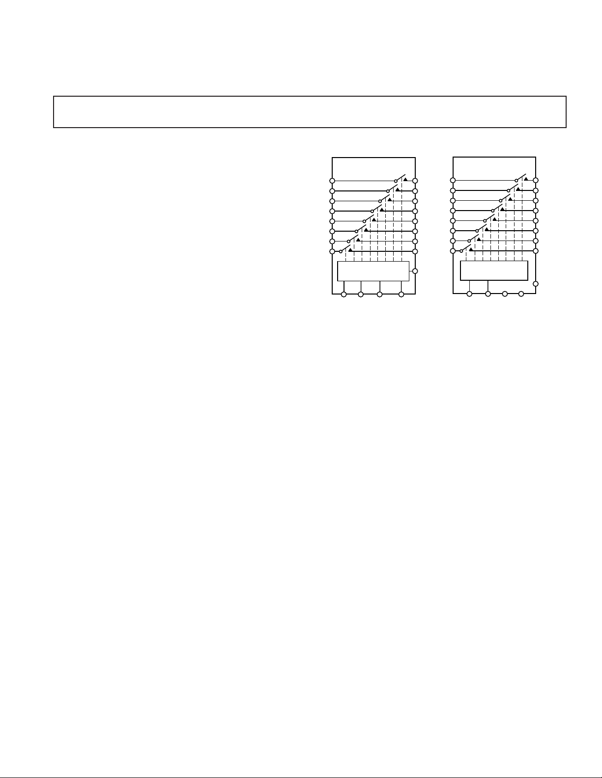
FUNCTIONAL BLOCK DIAGRAMS
ADG714
S1
S1
S2
S3
S4
S5
S6
S7
S8
INPUT SHIFT
REGISTER
SCLK DIN SYNC RESET
D1
D2
D3
D4
D5
D6
D7
D8
DOUT
S2
S3
S4
S5
S6
S7
S8
On power-up of these devices, all switches are in the OFF condition, and the internal registers contain all zeros.
Low power consumption and operating supply range of 2.7 V to
5.5 V make this part ideal for many applications. These parts
may also be supplied from a dual ±2.5 V supply. The ADG714
and ADG715 are available in a small 24-lead TSSOP package.
PRODUCT HIGHLIGHTS
1. 2- or 3-wire serial interface
2. Single/dual supply operation. The ADG714 and ADG715
are fully specified and guaranteed with 3 V, 5 V, and ±2.5 V
supply rails.
3. Low on resistance, typically 2.5 Ω
4. Low leakage
5. Power-on reset
6. Small 24-lead TSSOP package
ADG715
INTERFACE
LOGIC
SDA SCL A0 A1
D1
D2
D3
D4
D5
D6
D7
D8
RESET
SPI and QSPI are trademarks of Motorola, Inc.
MICROWIRE is a trademark of National Semiconductor Corporation.
I2C is a trademark of Philips Corporation.
REV. B
Information furnished by Analog Devices is believed to be accurate and
reliable. However, no responsibility is assumed by Analog Devices for its
use, nor for any infringements of patents or other rights of third parties that
may result from its use. No license is granted by implication or otherwise
under any patent or patent rights of Analog Devices.
One Technology Way, P.O. Box 9106, Norwood, MA 02062-9106, U.S.A.
Tel: 781/329-4700 www.analog.com
Fax: 781/326-8703 © Analog Devices, Inc., 2002
1
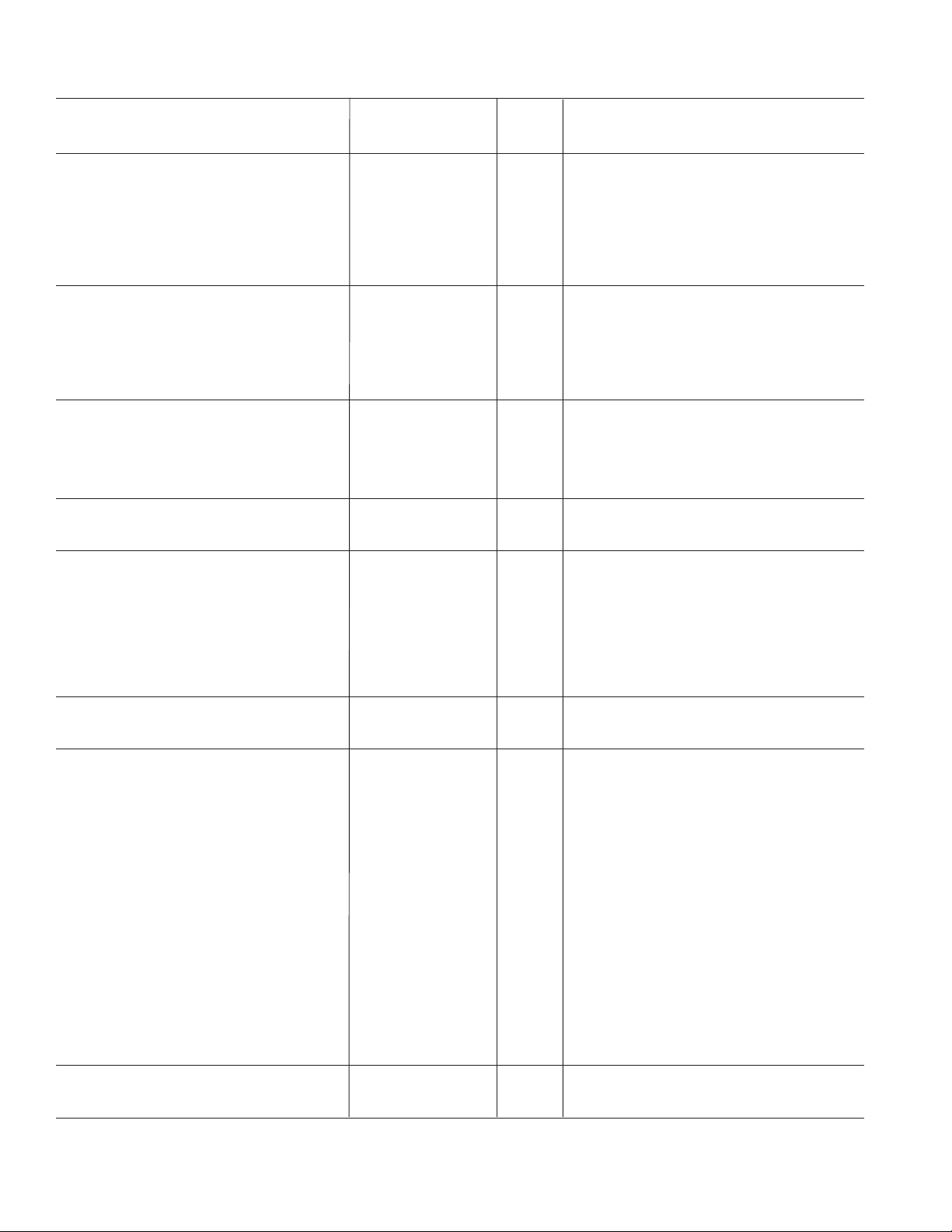
ADG714/ADG715–SPECIFICATIONS
B Version
–40C
Parameter +25C to +85CUnit Test Conditions/Comments
ANALOG SWITCH
Analog Signal Range 0 V to V
On Resistance (R
On Resistance Match Between Channels (∆R
On Resistance Flatness (R
LEAKAGE CURRENTS V
Source OFF Leakage I
Drain OFF Leakage I
Channel ON Leakage I
DIGITAL INPUTS (SCLK, DIN, SYNC, A0, A1)
Input High Voltage, V
Input Low Voltage, V
Input Current, I
CIN, Digital Input Capacitance
DIGITAL OUTPUT ADG714 DOUT
Output Low Voltage 0.4 V max I
C
Digital Output Capacitance 4 pF typ
OUT
DIGITAL INPUTS (SCL, SDA)
Input High Voltage, V
Input Low Voltage, V
I
, Input Leakage Current 0.005 µA typ VIN = 0 V to V
IN
V
, Input Hysteresis 0.05 V
HYST
CIN, Input Capacitance 6 pF typ
LOGIC OUTPUT (SDA)
VOL, Output Low Voltage 0.4 V max I
DYNAMIC CHARACTERISTICS
tON ADG714 20 ns typ VS = 3 V, RL = 300 Ω, CL = 35 pF
tON ADG715 95 ns typ VS = 3 V, RL = 300 Ω, CL = 35 pF
t
ADG714 8 ns typ VS = 3 V, RL = 300 Ω, CL = 35 pF
OFF
t
ADG715 85 ns typ VS = 3 V, RL = 300 Ω, CL = 35 pF
OFF
Break-Before-Make Time Delay, t
Charge Injection ± 3 pC typ VS = 2 V, RS = 0 Ω, CL = 1 nF
Off Isolation –60 dB typ
Channel-to-Channel Crosstalk –70 dB typ
–3 dB Bandwidth 155 MHz typ RL = 50 Ω, CL = 5 pF
(OFF) 11 pF typ
C
S
C
(OFF) 11 pF typ
D
CD, CS (ON) 22 pF typ
POWER REQUIREMENTS V
I
DD
NOTES
1
Temperature range is as follows: B Version: –40°C to +85°C.
2
Guaranteed by design, not subject to production test.
Specifications subject to change without notice.
)2.5Ω typ VS = 0 V to VDD, IS = 10 mA
ON
4.5 5 Ω max
)0.4Ω typ
ON
0.8 Ω max V
)0.6 Ω typ VS = 0 V to VDD, IS = 10 mA
FLAT(ON)
1.2 Ω max
(OFF) ± 0.01 nA typ VD = 4.5 V/1 V, VS = 1 V/4.5 V
S
± 0.1 ± 0.3 nA max
(OFF) ± 0.01 nA typ VD = 4.5 V/1 V, VS = 1 V/4.5 V
D
± 0.1 ± 0.3 nA max
, IS (ON) ± 0.01 nA typ VD = VS = 1 V, or 4.5 V
D
± 0.1 ± 0.3 nA max
2.4 V min
0.8 V max
± 0.1 µA max
0.7 V
V
DD
–0.3 V min
INL
or I
INH
INL
INH
INL
INH
0.005 µA typ VIN = V
2
2
2
3 pF typ
0.3 V
± 1 µA max
DD
2
0.6 V max I
2
32 ns max
140 ns max
15 ns max
130 ns max
D
8 ns typ VS = 3 V, RL = 300 Ω, CL = 35 pF
1 ns min
–80 dB typ R
–90 dB typ R
10 µA typ Digital Inputs = 0 V or 5.5 V
20 µA max
(VDD = 5 V 10%, VSS = 0 V, GND = 0 V unless otherwise noted.)
V
DD
= 0 V to VDD, IS = 10 mA
S
= 5.5 V
DD
or V
INL
INH
= 6 mA
SINK
V min
DD
+ 0.3 V max
V max
DD
DD
V min
= 3 mA
SINK
= 6 mA
SINK
RL = 50 Ω, CL = 5 pF, f = 10 MHz
= 50 Ω, CL = 5 pF, f = 1 MHz
L
RL = 50 Ω, CL = 5 pF, f = 10 MHz
= 50 Ω, CL = 5 pF, f = 1 MHz
L
= 5.5 V
DD
–2–
REV. B
1
ADG714/ADG715
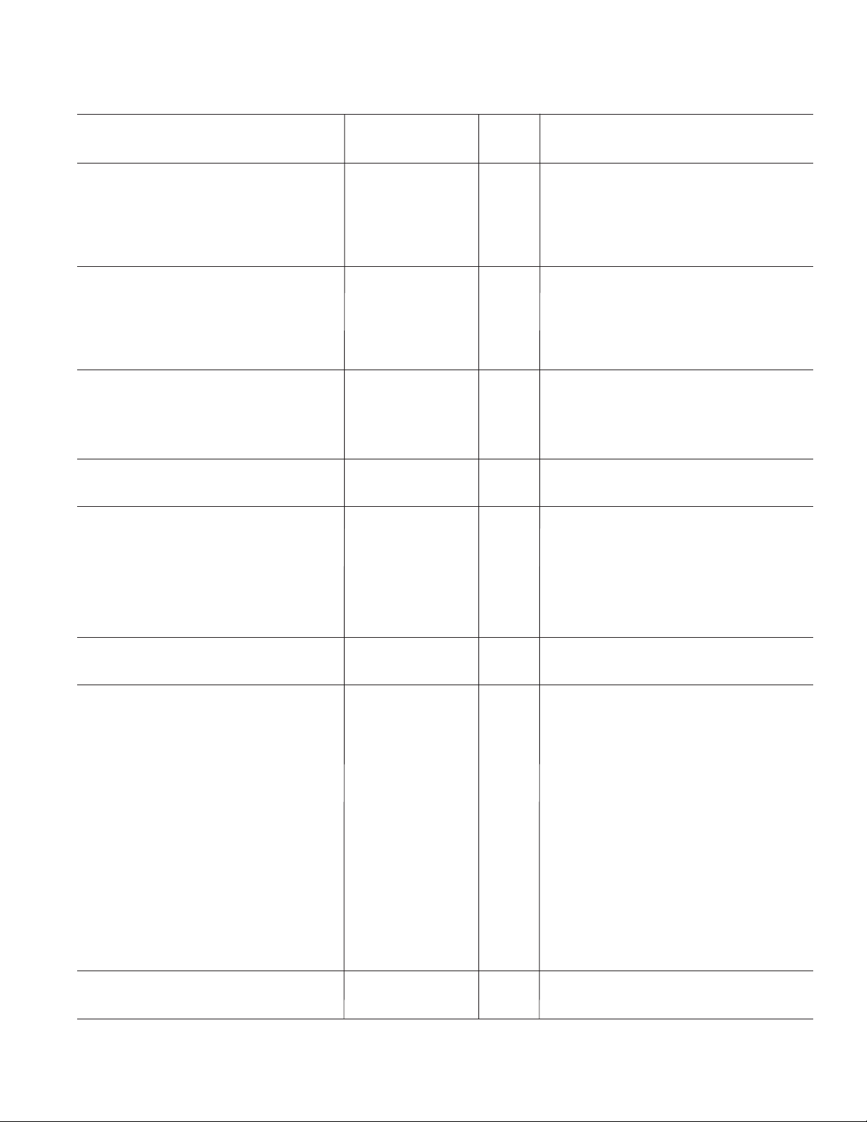
SPECIFICATIONS
Parameter +25C to +85CUnit Test Conditions/Comments
ANALOG SWITCH
Analog Signal Range 0 V to V
On Resistance (R
On Resistance Match Between Channels (∆RON) 0.4 Ω typ VS = 0 V to VDD, IS = 10 mA
On Resistance Flatness (R
LEAKAGE CURRENTS V
Source OFF Leakage I
Drain OFF Leakage ID (OFF) ± 0.01 nA typ VS = 1 V/3 V, VD = 3 V/1 V
Channel ON Leakage I
DIGITAL INPUTS (SCLK, DIN, SYNC, A0, A1)
Input High Voltage, V
Input Low Voltage, V
Input Current, I
CIN, Digital Input Capacitance
DIGITAL OUTPUT ADG714 DOUT
Output Low Voltage 0.4 V max I
C
Digital Output Capacitance 4 pF typ
OUT
DIGITAL INPUTS (SCL, SDA)
Input High Voltage, V
Input Low Voltage, V
IIN, Input Leakage Current 0.005 µA typ VIN = 0 V to V
V
, Input Hysteresis 0.05 V
HYST
CIN, Input Capacitance 6 pF typ
LOGIC OUTPUT (SDA)
VOL, Output Low Voltage 0.4 V max I
DYNAMIC CHARACTERISTICS
tON ADG714 35 ns typ VS = 2 V, RL = 300 Ω, CL = 35 pF
tON ADG715 130 ns typ VS = 2 V, RL = 300 Ω, CL = 35 pF
t
ADG714 11 ns typ VS = 2 V, RL = 300 Ω, CL = 35 pF
OFF
t
ADG715 115 ns typ VS = 2 V, RL = 300 Ω, CL = 35 pF
OFF
Break-Before-Make Time Delay, t
Charge Injection ± 2 pC typ VS = 1.5 V, RS = 0 Ω, CL = 1 nF
Off Isolation –60 dB typ
Channel-to-Channel Crosstalk –70 dB typ
–3 dB Bandwidth 155 MHz typ RL = 50 Ω,
CS (OFF) 11 pF typ
CD (OFF) 11 pF typ
CD, CS (ON) 22 pF typ
POWER REQUIREMENTS V
I
DD
NOTES
1
Temperature range is as follows: B Version: –40°C to +85°C.
2
Guaranteed by design, not subject to production test.
Specifications subject to change without notice.
REV. B
)6Ω typ VS = 0 V to VDD, IS = 10 mA
ON
FLAT(ON)
(OFF) ± 0.01 nA typ VS = 3 V/1 V, VD = 1 V/3 V
S
, IS (ON) ± 0.01 nA typ VS = VD = 1 V, or 3 V
D
INH
INL
or I
INL
INH
INH
INL
2
(VDD = 3 V 10%, VSS = 0 V, GND = 0 V unless otherwise noted.)
B Version
11 12 Ω max
) 3.5 Ω typ VS = 0 V to VDD, IS = 10 mA
± 0.1 ± 0.3 nA max
± 0.1 ± 0.3 nA max
± 0.1 ± 0.3 nA max
0.005 µA typ VIN = V
2
2
2
2
D
3 pF typ
8 ns typ VS = 2 V, RL = 300 Ω, CL = 35 pF
–80 dB typ RL = 50 Ω, CL = 5 pF, f = 1 MHz
–90 dB typ RL = 50 Ω, CL = 5 pF, f = 1 MHz
10 µA typ Digital Inputs = 0 V or 3.3 V
–40C
V
DD
1.2 Ω max
2.0 V min
0.8 V max
± 0.1 µA max
0.7 V
DD
V min
VDD + 0.3 V max
–0.3 V min
0.3 V
DD
V max
± 1 µA max
DD
V min
0.6 V max I
65 ns max
200 ns max
20 ns max
180 ns max
1 ns min
20 µA max
= 3.3 V
DD
or V
INL
INH
= 6 mA
SINK
DD
= 3 mA
SINK
= 6 mA
SINK
RL = 50 Ω, CL = 5 pF, f = 10 MHz
RL = 50 Ω, CL = 5 pF, f = 10 MHz
CL =
5 pF
= 3.3 V
DD
–3–
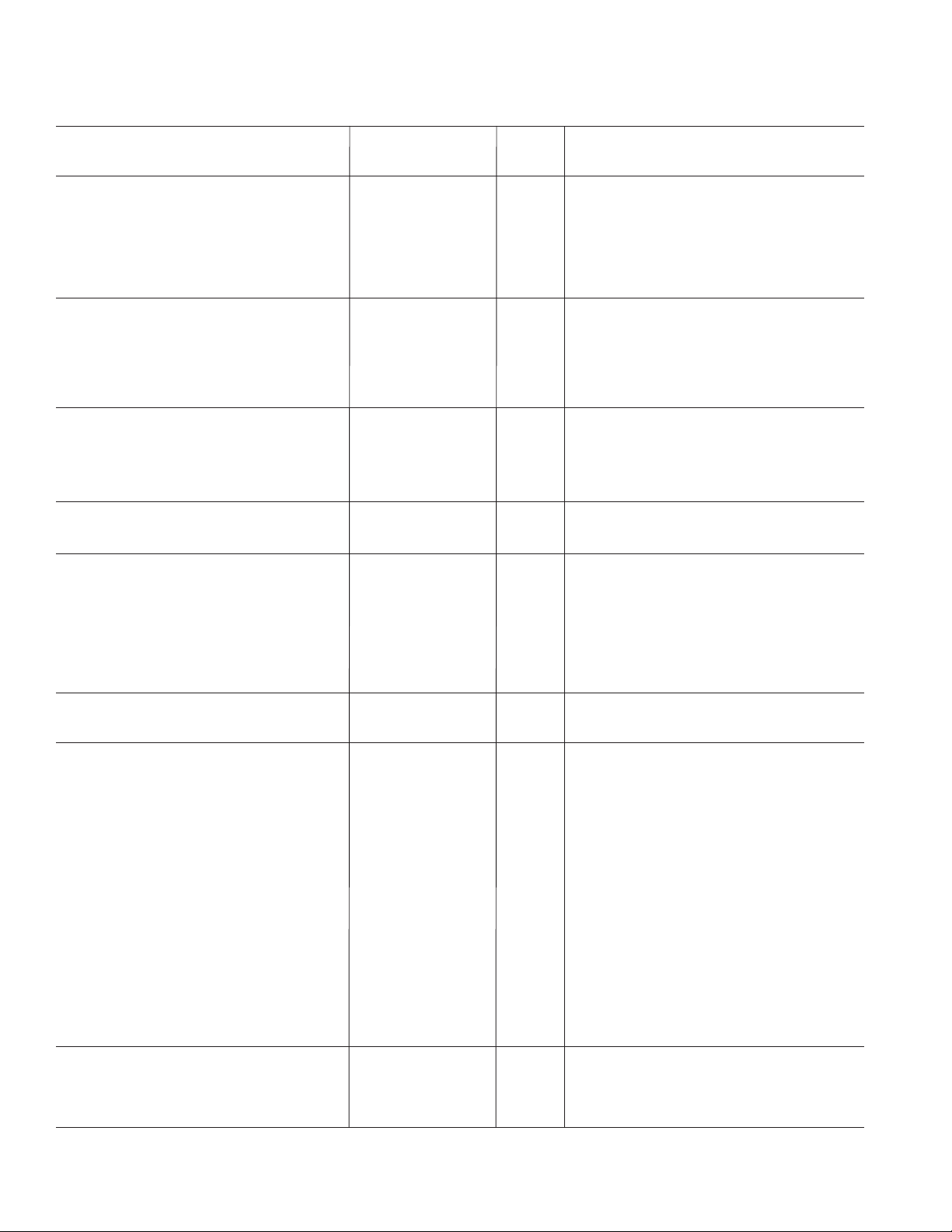
ADG714/ADG715–SPECIFICATIONS
1
DUAL SUPPLY
(VDD = +2.5 V 10%, VSS = 2.5 V 10%, GND = 0 V unless otherwise noted.)
B Version
–40C
Parameter +25C to +85C Unit Test Conditions/Comments
ANALOG SWITCH
Analog Signal Range V
On Resistance (R
) 2.5 Ω typ VS = VSS to VDD, IDS = 10 mA
ON
to VDDV
SS
4.5 5 Ω max
On Resistance Match Between Channels (∆R
) 0.4 Ω typ VS = VSS to VDD, IDS = 10 mA
ON
0.8 Ω max
On Resistance Flatness (R
) 0.6 Ω typ VS = VSS to VDD, IDS = 10 mA
FLAT(ON)
1 Ω max
LEAKAGE CURRENTS V
Source OFF Leakage I
(OFF) ± 0.01 nA typ VS = +2.25 V/–1.25 V, VD = –1.25 V/+2.25 V
S
= +2.75 V, VSS = –2.75 V
DD
± 0.1 ± 0.3 nA max
Drain OFF Leakage I
(OFF) ± 0.01 nA typ VS = +2.25 V/–1.25 V, VD = –1.25 V/+2.25 V
D
± 0.1 ± 0.3 nA max
Channel ON Leakage I
, IS (ON) ± 0.01 nA typ VS = VD = +2.25 V/–1.25 V
D
± 0.1 ± 0.3 nA max
DIGITAL INPUTS
Input High Voltage, V
Input Low Voltage, V
Input Current, I
CIN, Digital Input Capacitance
DIGITAL OUTPUT ADG714 DOUT
INL
or I
INH
INL
INH
0.005 µA typ VIN = V
2
2
3 pF typ
Output Low Voltage 0.4 V max
C
Digital Output Capacitance 4 pF typ
OUT
DIGITAL INPUTS (SCL, SDA)
Input High Voltage, V
Input Low Voltage, V
I
, Input Leakage Current 0.005 µA typ VIN = 0 V to V
IN
INH
INL
2
1.7 V min
0.7 V max
± 0.1 µA max
0.7 V
V
+ 0.3 V max
DD
DD
V min
–0.3 V min
0.3 V
DD
V max
I
SINK
or V
INL
= 6 mA
INH
DD
± 1 µA max
V
, Input Hysteresis 0.05 V
HYST
DD
V min
CIN, Input Capacitance 6 pF typ
LOGIC OUTPUT (SDA)
VOL, Output Low Voltage 0.4 V max I
DYNAMIC CHARACTERISTICS
2
= 3 mA
2
0.6 V max I
SINK
SINK
= 6 mA
tON ADG714 20 ns typ VS = 1.5 V, RL = 300 Ω, CL = 35 pF
32 ns max
t
ADG715 133 ns typ VS = 1.5 V, RL = 300 Ω, CL = 35 pF
ON
200 ns max
t
ADG714 8 ns typ VS = 1.5 V, RL = 300 Ω, CL = 35 pF
OFF
18 ns max
t
ADG715 124 ns typ VS = 1.5 V, RL = 300 Ω, CL = 35 pF
OFF
190 ns max
Break-Before-Make Time Delay, t
D
8 ns typ VS = 1.5 V, RL = 300 Ω, CL = 35 pF
1 ns min
Charge Injection ± 3 pC typ V
Off Isolation –60 dB typ
–80 dB typ R
Channel-to-Channel Crosstalk –70 dB typ
–90 dB typ R
= 0 V, RS = 0 Ω, CL = 1 nF
S
RL = 50 Ω, CL = 5 pF, f = 10 MHz
= 50 Ω, CL = 5 pF, f = 1 MHz
L
RL = 50 Ω, CL = 5 pF, f = 10 MHz
= 50 Ω, CL = 5 pF, f = 1 MHz
L
–3 dB Bandwidth 155 MHz typ RL = 50 Ω, CL = 5 pF
C
(OFF) 11 pF typ
S
C
(OFF) 11 pF typ
D
CD, CS (ON) 22 pF typ
POWER REQUIREMENTS V
I
DD
15 µA typ Digital Inputs = 0 V or 3.3 V
= +2.75 V, VSS = –2.75 V
DD
25 µA max
I
SS
15 µA typ
25 µA max
NOTES
1
Temperature range is as follows: B Version: –40°C to +85°C.
2
Guaranteed by design, not subject to production test.
Specifications subject to change without notice.
–4–
REV. B
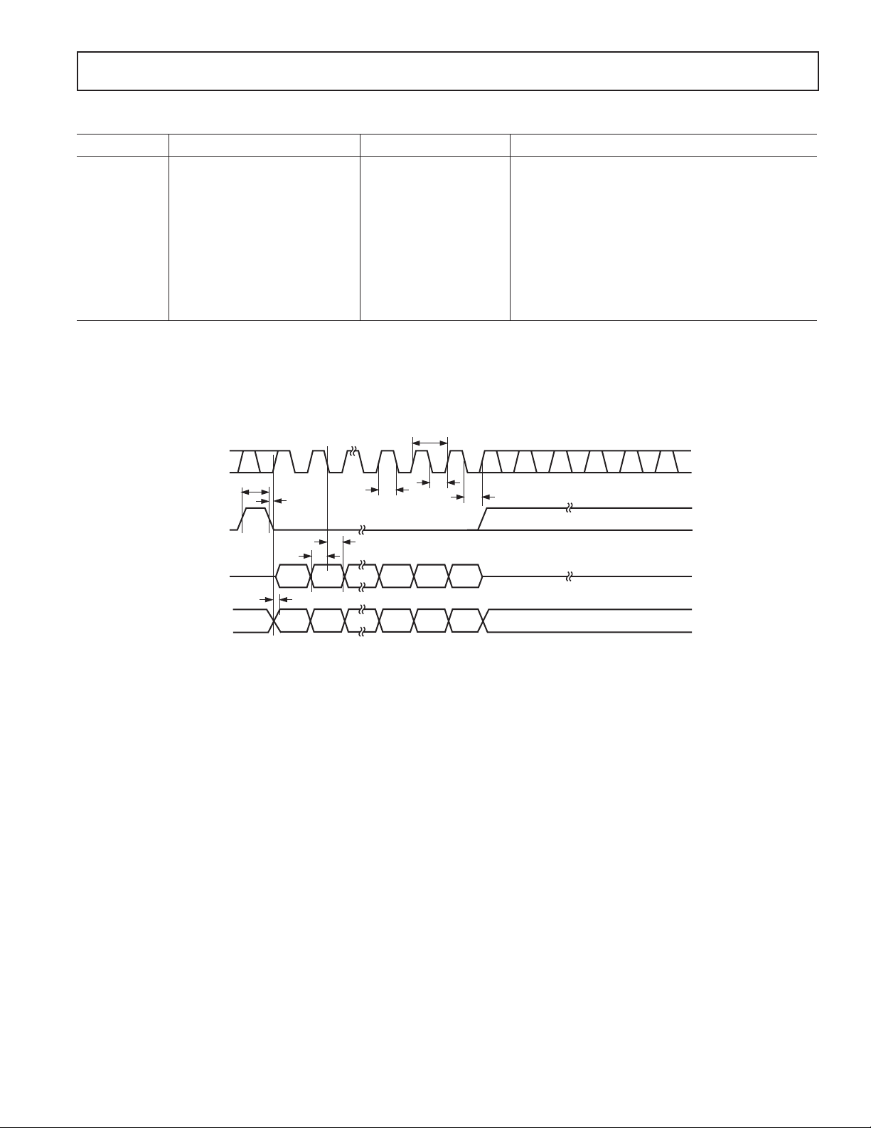
ADG714/ADG715
ADG714 TIMING CHARACTERISTICS
Parameter Limit at T
f
SCLK
t
1
t
2
t
3
t
4
t
5
t
6
t
7
t
8
3
t
9
NOTES
1
See Figure 1.
2
All input signals are specified with tr = tf = 5 ns (10% to 90% of VDD) and timed from a voltage level of (VIL + VIH)/2.
3
CL = 20 pF, RL = 1 kΩ.
Specifications subject to change without notice.
30 MHz max SCLK Cycle Frequency
33 ns min SCLK Cycle Time
13 ns min SCLK High Time
13 ns min SCLK Low Time
0 ns min SYNC to SCLK Rising Edge Setup Time
5 ns min Data Setup Time
4.5 ns min Data Hold Time
0 ns min SCLK Falling Edge to SYNC Rising Edge
33 ns min Minimum SYNC High Time
20 ns max SCLK Rising Edge to DOUT Valid
SCLK
SYNC
DIN
DOUT
t
8
, T
MIN
t
DB7*DB6
4
t
9
MAX
t
5
1, 2
(VDD = 2.7 V to 5.5 V. All specifications –40C to +85C unless otherwise noted.)
Unit Conditions/Comments
t
1
t
t
2
t
6
*
DB2*DB1*DB0
3
t
7
DB0DB7
*
*
DATA FROM PREVIOUS WRITE CYCLE
Figure 1. 3-Wire Serial Interface Timing Diagram
REV. B
–5–
 Loading...