

CMOS Low Voltage
S
www.BDTIC.com/ADI
FEATURES
1.8 V to 5.5 V single supply
2 Ω (typical) on resistance
Low on resistance flatness
Guaranteed leakage specifications up to 85°C
–3 dB bandwidth > 200 MHz
Rail-to-rail operation
Fast switching times
18 ns
t
ON
t
12 ns
OFF
Typical power consumption < 0.01 μW
TTL/CMOS-compatible
APPLICATIONS
Battery-powered systems
Communication systems
Sample-and-hold systems
Audio signal routing
Video switching
Mechanical reed relay replacement
GENERAL DESCRIPTION
2 Ω SPST Switches
ADG701L/ADG702L
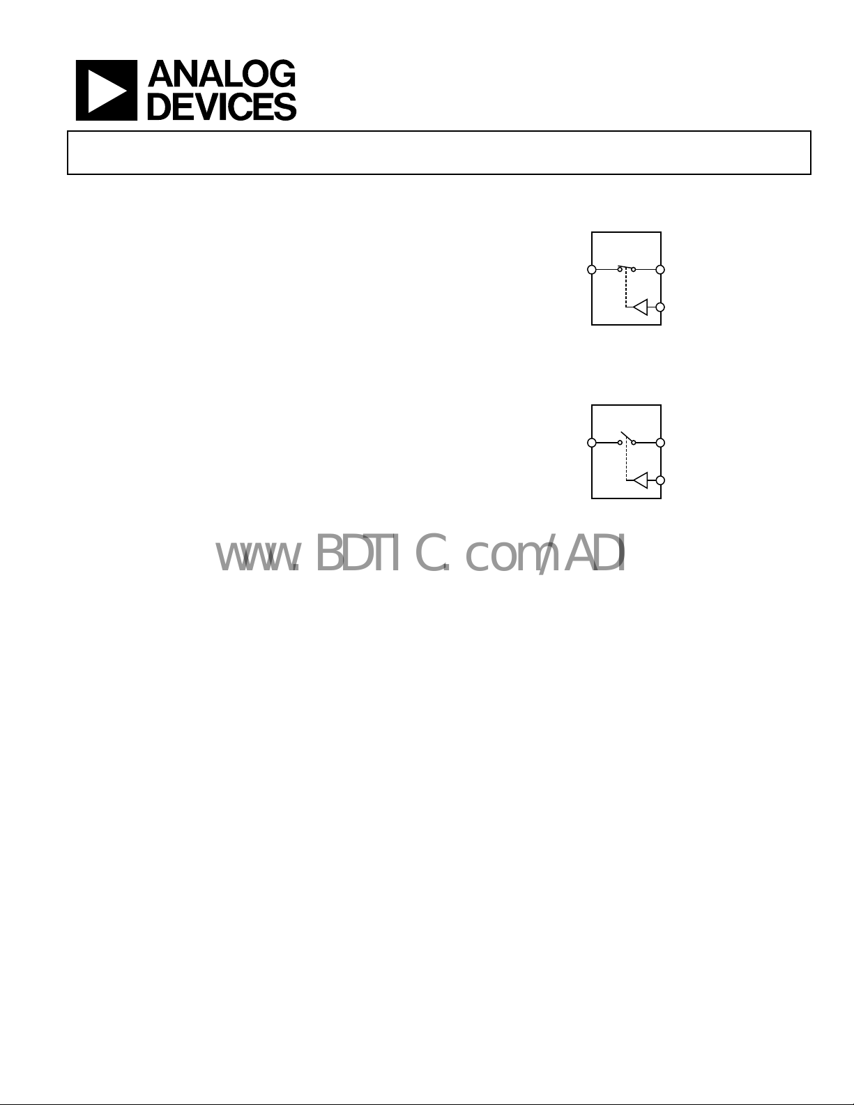
FUNCTIONAL BLOCK DIAGRAMS
ADG701L
SWITCHES SHOWN
FOR A LOGIC 1 INPUT
ADG702L
SWITCHES SHOWN
FOR A LOGIC 1 INPUT
PRODUCT HIGHLIGHTS
Figure 1.
Figure 2.
D
IN
05486-001
DS
IN
05486-020
The ADG701L/ADG702L are monolithic CMOS SPST switches.
These switches are designed using an advanced submicron
process that provides low power dissipation, yet offers high
switching speed, low on resistance, and low leakage currents.
In addition, −3 dB bandwidths of greater than 200 MHz can
be achieved.
The ADG701L/ADG702L can operate from a single 1.8 V to
5.5 V s
upply, making it ideal for use in battery-powered
instruments and with the new generation of DACs and ADCs
from Analog Devices.
Figure 1 and Figure 2 show that with a logic input of 1, the
tch of the ADG701L is closed, while that of the ADG702L
swi
is open. Each switch conducts equally well in both directions
when on.
The ADG701L/ADG702L are packaged as 5-lead SOT-23,
6-lead S
OT-23, and 8-lead MSOP.
Rev. 0
Information furnished by Analog Devices is believed to be accurate and reliable. However, no
responsibility is assumed by Anal og Devices for its use, nor for any infringements of patents or ot her
rights of third parties that may result from its use. Specifications subject to change without notice. No
license is granted by implication or otherwise under any patent or patent rights of Analog Devices.
Trademarks and registered trademarks are the property of their respective owners.
1. 1.8 V to 5.5 V single-supply operation. The ADG701L/
ADG702L offer high performance, including low on
resistance and fast switching times. The ADG701L/
ADG702L are fully specified and guaranteed with 3 V
and 5 V supply rails.
r y low R
2. Ve
At 1.8 V operation, R
(3 Ω maximum at 5 V, 5 Ω maximum at 3 V).
ON
is typically 40 Ω over the
ON
temperature range.
n resistance flatness R
3. O
4. −3 dB ban
5. L
ow power dissipation. CMOS construction ensures low
dwidth > 200 MHz.
(1 Ω maximum).
FLAT(ON)
power dissipation.
6. Fa
st t
One Technology Way, P.O. Box 9106, Norwood, MA 02062-9106, U.S.A.
Tel: 781.329.4700 www.analog.com
Fax: 781.461.3113 ©2006 Analog Devices, Inc. All rights reserved.
ON/tOFF
.

ADG701L/ADG702L
www.BDTIC.com/ADI
TABLE OF CONTENTS
Features.............................................................................................. 1
Typical Performance Characteristics..............................................7
Applications....................................................................................... 1
General Description ......................................................................... 1
Functional Block Diagrams............................................................. 1
Product Highlights ........................................................................... 1
Revision History ............................................................................... 2
Specifications..................................................................................... 3
Absolute Maximum Ratings............................................................ 5
ESD Caution.................................................................................. 5
Pin Configurations and Function Descriptions ........................... 6
REVISION HISTORY
11/06—Revision 0: Initial Version
Test Circuits........................................................................................8
Terminology.......................................................................................9
Applications Information.............................................................. 10
Supply Voltages ........................................................................... 10
Bandwidth ................................................................................... 10
Off Isolation ................................................................................ 10
Outline Dimensions....................................................................... 11
Ordering Guide .......................................................................... 12
Rev. 0 | Page 2 of 12
ADG701L/ADG702L
www.BDTIC.com/ADI
SPECIFICATIONS
VDD = 5 V ± 10%, GND = 0 V. Temperature range for the B version is −40°C to +85°C, unless otherwise noted.
Table 1.
B Version
o
−40°C t
Parameter +25°C
+85°C
ANALOG SWITCH
Analog Signal Range 0 V to VDD V
On Resistance (RON) 2 Ω typ
3 4 Ω max
On Resistance Flatness (R
) 0.5 Ω typ
FLAT(ON)
1.0 Ω max
LEAKAGE CURRENTS VDD = 5.5 V
Source Off Leakage, IS (OFF) ±0.01 nA typ VS = 4.5 V/1 V, VD = 1 V/4.5 V; see Figure 13
±0.25 ±0.35 nA max
Drain Off Leakage, ID (OFF) ±0.01 nA typ VS = 4.5 V/1 V, VD = 1 V/4.5 V; see Figure 13
±0.25 ±0.35 nA max
Channel On Leakage, ID, IS (ON) ±0.01 nA typ VS = VD = 1 V, or 4.5 V; see Figure 14
±0.25 ±0.35 nA max
DIGITAL INPUTS
Input High Voltage, V
Input Low Voltage, V
2.4 V min
INH
0.8 V max
INL
Input Current
I
or I
0.005 μA typ VIN = V
INL
INH
±0.1 μA max
DYNAMIC CHARACTERISTICS
1
tON 12 ns typ RL = 300 Ω, CL = 35 pF
18 ns max VS = 3 V; see Figure 15
t
8 ns typ RL = 300 Ω, CL = 35 pF
OFF
12 ns max VS = 3 V; see Figure 15
Charge Injection 5 pC typ VS = 2 V, RS = 0 Ω, CL = 1 nF; see Figure 16
Off Isolation
Bandwidth −3 dB
−55
−75
200 MHz typ RL = 50 Ω, CL = 5 pF; see Figure 18
dB typ RL = 50 Ω, CL = 5 pF, f = 10 MHz
dB typ RL = 50 Ω, CL = 5 pF, f = 1 MHz; see Figure 17
CS (OFF) 17 pF typ
CD (OFF) 17 pF typ
CD, CS (ON) 38 pF typ
POWER REQUIREMENTS VDD = 5.5 V
IDD 0.001 μA typ Digital inputs = 0 V or 5 V
1.0 μA max
1
Guaranteed by design, not subject to production test.
Unit Test C
VS = 0 V to VDD, IS = −10 mA; see Figure 12
= 0 V to VDD, IS = −10 mA
V
S
onditions/Comments
or V
INH
INL
Rev. 0 | Page 3 of 12
ADG701L/ADG702L
www.BDTIC.com/ADI
VDD = 3 V ± 10%, GND = 0 V. Temperature range for the B version is −40°C to +85°C, unless otherwise noted.
Table 2.
B Version
o
−40°C t
Parameter +25°C
+85°C
ANALOG SWITCH
Analog Signal Range 0 V to VDD V
On Resistance (RON) 3.5 Ω typ
5 6 Ω max
On Resistance Flatness (R
) 1.5 Ω typ
FLAT(ON)
LEAKAGE CURRENTS VDD = 3.3 V
Source Off Leakage IS (OFF) ±0.01 nA typ VS = 3 V/1 V, VD = 1 V/3 V; see Figure 13
±0.25 ±0.35 nA max
Drain Off Leakage ID (OFF) ±0.01 nA typ VS = 3 V/1 V, VD = 1 V/3 V; see Figure 13
±0.25 ±0.35 nA max
Channel On Leakage ID, IS (ON) ±0.01 nA typ VS = VD = 1 V, or 3 V; see Figure 14
±0.25 ±0.35 nA max
DIGITAL INPUTS
Input High Voltage, V
Input Low Voltage, V
2.0 V min
INH
0.4 V max
INL
Input Current
I
or I
0.005 μA typ VIN = V
INL
INH
±0.1 μA max
DYNAMIC CHARACTERISTICS
1
tON 14 ns typ
20 ns max VS = 2 V, see Figure 15
t
8 ns typ
OFF
13 ns max VS = 2 V, see Figure 15
Charge Injection 4 pC typ
Off Isolation
Bandwidth −3 dB
−55
−75
200 MHz typ
dB typ
dB typ
CS (OFF) 17 pF typ
CD (OFF) 17 pF typ
CD, CS (ON) 38 pF typ
POWER REQUIREMENTS VDD = 3.3 V
IDD 0.001 μA typ Digital Inputs = 0 V or 3 V
1.0 μA max
1
Guaranteed by design, not subject to production test.
Unit Test Conditions/Comments
VS = 0 V to VDD, IS = −10 mA; see Figure 12
VS = 0 V to VDD, IS = −10 mA
or V
INH
INL
RL = 300 Ω, CL = 35 pF
RL = 300 Ω, CL = 35 pF
VS = 1.5 V, RS = 0 Ω, CL = 1 nF; see Figure 16
RL = 50 Ω, CL = 5 pF, f = 10 MHz
RL = 50 Ω, CL = 5 pF, f = 1 MHz; see Figure 17
RL = 50 Ω, CL = 5 pF; see Figure 18
Rev. 0 | Page 4 of 12

ADG701L/ADG702L
www.BDTIC.com/ADI
ABSOLUTE MAXIMUM RATINGS
TA = 25°C, unless otherwise noted.
Table 3.
Parameter Rating
VDD to GND
Analog, Digital Inputs
Continuous Current, S or D 30 mA
Peak Current, S or D
Operating Temperature Range
Industrial (B Version)
Storage Temperature Range
Junction Temperature 150°C
MSOP Package, Power Dissipation 315 mW
θJA Thermal Impedance 206°C/W
θJC Thermal Impedance 44°C/W
SOT-23 Package, Power Dissipation 282 mW
θJA Thermal Impedance 229.6°C/W
θJC Thermal Impedance 91.99°C/W
Lead Temperature, Soldering
Vapor Phase (60 sec) 215°C
Infrared (15 sec) 220°C
Lead-free Reflow Soldering
Peak Temperature 260 (+0/−5)°C
Time at Peak Temperature 10 sec to 40 sec
ESD 2 kV
1
Overvoltages at IN, S, or D are clamped by internal diodes. Current should be
limited to the maximum ratings given.
1
−0.3 V to +7 V
−0.3 V to VDD + 0.3 V or 30 mA,
whichever occurs first
100 mA, pulsed at 1 ms,
10% duty c
−40°C to +85°C
−65°C to +150°C
ycle maximum
Stresses above those listed under Absolute Maximum Ratings
ma
y cause permanent damage to the device. This is a stress
rating only; functional operation of the device at these or any
other conditions above those indicated in the operational
section of this specification is not implied. Exposure to absolute
maximum rating conditions for extended periods may affect
device reliability.
ESD CAUTION
ESD (electrostatic discharge) sensitive device. Electrostatic charges as high as 4000 V readily accumulate on
the human body and test equipment and can discharge without detection. Although this product features
proprietary ESD protection circuitry, permanent damage may occur on devices subjected to high energy
electrostatic discharges. Therefore, proper ESD precautions are recommended to avoid performance degradation or loss of functionality.
Rev. 0 | Page 5 of 12

ADG701L/ADG702L
V
G
G
www.BDTIC.com/ADI
PIN CONFIGURATIONS AND FUNCTION DESCRIPTIONS
1
D
ADG701L/
NC
2
ADG702L
NC
3
TOP VIEW
4
(Not to Scale)
DD
NC = NO CONNECT
Figure 3. 8-Lead MSOP Pin Configuration Figure 4. 6-Lead SOT
S
8
GND
7
IN
6
5
NC
05486-002
D
1
ADG701L/
2
S
ADG702L
TOP VIEW
ND
3
(Not to Scale)
NC = NO CONNECT
V
6
DD
5
NC
IN
4
05486-003
D
S
ND
1
ADG701L/
2
ADG702L
TOP VIEW
3
(Not to Scale)
V
5
DD
4
IN
-23 Pin Configuration Figure 5. 5-Lead SOT-23 Pin Configuration
Table 4. Pin Function Descriptions
Pin Number
8-Lead MSOP 6-lead SOT-23 5-lead SOT-23
Mnemonic Description
1 1 1 D Drain Terminal. May be an input or output.
2, 3, 5 5 N/A NC No Connect.
4 6 5 VDD Most Positive Power Supply Potential.
6 4 4 IN Logic Control Input.
7 3 3 GND Ground (0 V) Reference.
8 2 2 S Source Terminal. May be an input or output.
Table 5. Truth Table
ADG701L In ADG702L In Switch Condition
0 1 Off
1 0 On
05486-004
Rev. 0 | Page 6 of 12

ADG701L/ADG702L
www.BDTIC.com/ADI
TYPICAL PERFORMANCE CHARACTERISTICS
3.5
3.0
VDD = 2.7V
T
A
= 25°C
10m
1m
VDD = 5V
2.5
= 3.0V
V
2.0
(Ω)
ON
1.5
R
1.0
0.5
0
0 0.5 1.0 1.5 2.0 2.5 3.0 3.5 4.0 4.5 5.0
DD
V
= 5.0V
DD
VD OR VS (DRAIN OR SOURCE VOLTAGE (V))
V
= 4.5V
DD
Figure 6. On Resistance as a Function of VD (VS) Single Supplies
3.5
V
= 3V
3.0
2.5
2.0
(Ω)
ON
1.5
R
1.0
0.5
0
0 0.5 1.0 1.5 2.0 2.5 3.0
VD OR VS (DRAIN OR SOURCE VOLTAGE (V))
+85°C
+25°C
–40°C
DD
Figure 7. On Resistance as a Function of VD (VS) for Different
Temperatures V
3.5
3.0
DD
= 3 V
VDD = 5V
05486-005
05486-006
100μ
10μ
(A)
1μ
SUPPLY
I
100n
10n
1n
10 100 1k 10k 100k 1M 10M
FREQUENCY (Hz)
Figure 9. Supply Current vs. Input Switching Frequency
–10
VDD = 5V, 3V
–20
–30
–40
–50
–60
–70
–80
OFF ISOLATION (dB)
–90
–100
–110
10k 100k 1M 10M 100M
FREQUENCY (Hz)
Figure 10. Off Isolation vs. Frequency
0
VDD = 3V
05486-008
05486-009
2.5
2.0
(Ω)
ON
1.5
R
1.0
0.5
0
0 0.5 1.0 1.5 2.0 2.5 3.0 3.5 4.0 4.5 5.0
VD OR VS (DRAIN OR SOURCE VOLTAGE (V))
Figure 8. On Resistance as a Function of V
+85°C
+25°C
–40°C
Temperatures V
DD
= 5 V
(VS) for Different
D
05486-007
Rev. 0 | Page 7 of 12
–2
–4
ON RESPONSE (dB)
–6
10k 100k 1M 10M 100M
FREQUENCY (Hz)
05486-010
Figure 11. Bandwidth

ADG701L/ADG702L
V
V
V
V
www.BDTIC.com/ADI
TEST CIRCUITS
I
DS
V1
SD
IS(OFF) ID(OFF)
SD
A A
SD
ID (ON)
A
V
S
RON = V1/I
DS
05486-011
S
V
D
05486-012
S
V
D
05486-013
Figure 12. On Resistance Figure 13. Off Leakage Figure 14. On Leakage
V
DD
0.1μF
V
IN
V
OUT
V
IN
ADG701L
ADG702L
V
DD
V
C
L
35pF
OUT
SD
R
V
S
IN
GND
L
300Ω
50% 50%
50% 50%
90% 90%
t
ON
t
OFF
05486-014
Figure 15. Switching Times
V
DD
V
DD
R
S
V
S
S
IN
GND
D
C
L
1nF
V
ADG701L
IN
V
OUT
V
ADG702L
IN
V
OUT
ON OFF
= CL×ΔV
Q
INJ
OUT
ΔV
OUT
05486-015
Figure 16. Charge Injection
DD
0.1μF
V
DD
V
R
50Ω
OUT
L
05486-016
SD
IN
V
V
S
IN
GND
Figure 17. Off Isolation
Rev. 0 | Page 8 of 12
V
DD
0.1μF
V
DD
V
R
50Ω
OUT
L
05486-017
SD
IN
V
S
IN
GND
Figure 18. Bandwidth

ADG701L/ADG702L
www.BDTIC.com/ADI
TERMINOLOGY
R
ON
Ohmic resistance between D and S.
R
FLAT (ON)
Flatness is defined as the difference between the maximum and
minimum value of on resistance as measured over the specified
analog signal range.
t
ON
Delay between applying the digital control input and the output
switching on. See Figure 15.
t
OFF
Delay between applying the digital control input and the output
switching off.
(OFF)
I
S
Source leakage current with the switch off.
(OFF)
I
D
Drain leakage current with the switch off.
I
, IS (ON)
D
Channel leakage current with the switch on.
V
(VS)
D
Analog voltage on Terminal D and Terminal S.
(OFF)
C
S
Off switch source capacitance.
C
(OFF)
D
Off switch drain capacitance.
C
, CS (ON)
D
On switch capacitance.
Off Isolation
ure of unwanted signal coupling through an off switch.
A meas
Charge Injection
asure of the glitch impulse transferred from the digital
A me
input to the analog output during switching.
Bandwidth
requency at which the output is attenuated by −3 dB.
The f
On Response
T
he frequency response of the on switch.
On Loss
The v
oltage drop across the on switch, seen in Figure 11 as
th
e number of decibels the signal is away from 0 dB at very low
frequencies.
Rev. 0 | Page 9 of 12

ADG701L/ADG702L
www.BDTIC.com/ADI
APPLICATIONS INFORMATION
The ADG701L/ADG702L belong to the Analog Devices new
family of CMOS switches. This series of general-purpose switches
have improved switching times, lower on resistance, higher
bandwidth, low power consumption, and low leakage currents.
SUPPLY VOLTAGES
Functionality of the ADG701L/ADG702L extends from 1.8 V to
5.5 V single supply, making the parts ideal for battery-powered
instruments where power, efficiency, and performance are
important design parameters.
It is important to note that the supply voltage affects the input
sig
nal range, the on resistance, and the switching times of the
part. The effects of the power supplies can be clearly seen in the
Typical Performance Characteristics and the Specifications
ons.
secti
For V
= 1.8 V operation, RON is typically 40 Ω over the
DD
temperature range.
BANDWIDTH
Figure 19 illustrates the parasitic components that affect the ac
performance of CMOS switches (a box surrounds the switch).
Additional external capacitances further degrade some performance. These capacitances affect feedthrough, crosstalk, and
system bandwidth.
C
DS
SD
R
ON
V
IN
Figure 19. Switch Represented by Equiva
C
C
D
LOADRLOAD
lent Parasitic Components
The transfer function that describes the equivalent diagram of
the switch (see Figure 19) is of the form A(s), as shown in the
lowing equation:
fol
⎡
=
)(
RsA
⎢
T
⎣
CRs
ON
⎤
+
1)(
DSON
RCRs
⎥
+
1)(
TT
⎦
V
OUT
05486-018
The signal transfer characteristic is dependent on the switch
c
hannel capacitance, C
. This capacitance creates a frequency
DS
zero in the numerator of the transfer function, A(s). Because
the switch on resistance is small, this zero usually occurs at high
frequencies. The bandwidth is a function of the switch output
capacitance combined with C
and the load capacitance. The
DS
frequency pole corresponding to these capacitances appears in
the denominator of A(s).
The dominant effect of the output capacitance, C
, causes the
D
pole breakpoint frequency to occur first. In order to maximize
bandwidth, a switch must have a low input and output capacitance and low on resistance. The on response versus frequency
for the ADG701L/ADG702L is shown in
Figure 11.
OFF ISOLATION
Off isolation is a measure of the input signal coupled through
an off switch to the switch output. The capacitance, C
the input signal to the output load when the switch is off (see
Figure 20).
C
DS
SD
D
C
citance
LOADRLOAD
V
IN
Figure 20. Off Isolation Is Affected by External Load Resistance and
C
Capa
The larger the value of CDS, the larger the values of feedthrough
produced. Figure 10 illustrates the drop in off isolation as a
unction of frequency. From dc to roughly 1 MHz, the switch
f
shows better than −75 dB isolation. Up to frequencies of
10 MHz, the off isolation remains better than −55 dB. As the
frequency increases, more and more of the input signal is
coupled through to the output. Off isolation can be maximized
by choosing a switch with the smallest C
possible. The values
DS
of load resistance and capacitance also affect off isolation, as
they contribute to the coefficients of the poles and zeros in the
transfer function of the switch when open.
, couples
DS
V
OUT
05486-019
= C
where C
T
+ CD + CDS.
LOAD
Rev. 0 | Page 10 of 12
⎡
)(
=
RsA
⎢
T
⎣
CRs
LOAD
⎤
1)(
+
DSLOAD
CRs
⎥
1))((
+
T
⎦

ADG701L/ADG702L
www.BDTIC.com/ADI
OUTLINE DIMENSIONS
3.00
BSC
8
5
3.00
BSC
1
PIN 1
0.65 BSC
0.15
0.00
0.38
0.22
COPLANARITY
0.10
COMPLIANT TO JEDEC STANDARDS MO-187-AA
4.90
BSC
4
SEATING
PLANE
1.10 MAX
0.23
0.08
8°
0°
0.80
0.60
0.40
Figure 21. 8-Lead Mini Small Outline Package [MSOP]
(RM-8)
Dim
ensions shown in millimeters
2.90 BSC
4526
1.60 BSC
PIN 1
INDICATOR
1.30
1.15
0.90
0.15 MAX
1 3
1.90
BSC
0.50
0.30
COMPLIANT TO JEDEC STANDARDS MO-178-AB
2.80 BSC
0.95 BSC
1.45 MAX
SEATING
PLANE
0.22
0.08
Figure 22. 6-Lead Small Outline Transistor Package [SOT-23]
(RT-6)
Dim
ensions shown in millimeters
10°
0.60
4°
0.45
0°
0.30
2.90 BSC
1.60 BSC
1.30
1.15
0.90
0.15 MAX
5
123
PIN 1
COMPLIANT TO JEDEC STANDARDS MO-178-AA
1.90
BSC
0.50
0.30
4
2.80 BSC
0.95 BSC
1.45 MAX
SEATING
PLANE
0.22
0.08
10°
5°
0°
0.60
0.45
0.30
Figure 23. 5-Lead Small Outline Transistor Package [SOT-23]
(RJ-5)
Dim
ensions shown in millimeters
Rev. 0 | Page 11 of 12

ADG701L/ADG702L
www.BDTIC.com/ADI
ORDERING GUIDE
Model Temperature Range Package Description Package Option Branding
ADG701LBRJ-500RL7 −40°C to +85°C 5-Lead Small Outline Transistor Package [SOT-23] RJ-5 S15
ADG701LBRJ-REEL −40°C to +85°C 5-Lead Small Outline Transistor Package [SOT-23] RJ-5 S15
ADG701LBRJ-REEL7 −40°C to +85°C 5-Lead Small Outline
ADG701LBRJZ-500RL7
ADG701LBRJZ-REEL
ADG701LBRJZ-REEL7
2
−40°C to +85°C 5-Lead Small Outline Transistor Package [SOT-23] RJ-5 S10
2
−40°C to +85°C 5-Lead Small Outline Transistor Package [SOT-23] RJ-5 S10
2
−40°C to +85°C 5-Lead Small Outline Transistor Package [SOT-23] RJ-5 S10
ADG701LBRM −40°C to +85°C 8-Lead Mini Small Outline Package [MSOP] RM-8
ADG701LBRM-REEL −40°C to +85°C 8-Lead Mini Small Outline Package [MSOP] RM-8
ADG701LBRM-REEL7 −40°C to +85°C 8-Lead Mini Small Outline Package [MSOP] RM-8
ADG701LBRMZ
ADG701LBRMZ-REEL
ADG701LBRMZ-REEL7
2
−40°C to +85°C 8-Lead Mini Small Outline Package [MSOP] RM-8 S10
2
−40°C to +85°C 8-Lead Mini Small Outline Package [MSOP] RM-8 S10
2
−40°C to +85°C 8-Lead Mini Small Outline Package [MSOP] RM-8 S10
ADG701LBRT-REEL −40°C to +85°C 6-Lead Small Outline Transistor Package [SOT-23] RT-6
ADG701LBRT-REEL7 −40°C to +85°C 6-Lead Small Outline Transistor Package [SOT-23] RT-6
ADG701LBRTZ-REEL
ADG701LBRTZ-REEL7
2
−40°C to +85°C 6-Lead Small Outline Transistor Package [SOT-23] RT-6 S10
2
−40°C to +85°C 6-Lead Small Outline Transistor Package [SOT-23] RT-6 S10
ADG702LBRJ-REEL −40°C to +85°C 5-Lead Small Outline
ADG702LBRJ-REEL7 −40°C to +85°C 5-Lead Small Outline Transistor Package [SOT-23] RJ-5 S16
ADG702LBRJZ-500RL7
ADG702LBRJZ-REEL
ADG702LBRJZ-REEL7
2
−40°C to +85°C 5-Lead Small Outline Transistor Package [SOT-23] RJ-5 S11
2
−40°C to +85°C 5-Lead Small Outline Transistor Package [SOT-23] RJ-5 S11
2
−40°C to +85°C 5-Lead Small Outline Transistor Package [SOT-23] RJ-5 S11
ADG702LBRM −40°C to +85°C 8-Lead Mini Small Outline Package [MSOP] RM-8
ADG702LBRM-REEL −40°C to +85°C 8-Lead Mini Small Outline Package [MSOP] RM-8
ADG702LBRM-REEL7 −40°C to +85°C 8-Lead Mini Small Outline Package [MSOP] RM-8
ADG702LBRMZ
ADG702LBRMZ-REEL
ADG702LBRMZ-REEL7
2
−40°C to +85°C 8-Lead Mini Small Outline Package [MSOP] RM-8 S11
2
−40°C to +85°C 8-Lead Mini Small Outline Package [MSOP] RM-8 S11
2
−40°C to +85°C 8-Lead Mini Small Outline Package [MSOP] RM-8 S11
ADG702LBRT-REEL −40°C to +85°C 6-Lead Small Outline Transistor Package [SOT-23] RT-6
ADG702LBRT-REEL7 −40°C to +85°C 6-Lead Small Outline Transistor Package [SOT-23] RT-6
ADG702LBRTZ-REEL
ADG702LBRTZ-REEL7
1
Due to package size limitations, these three characters represent the part number.
2
Z = Pb-free part.
2
−40°C to +85°C 6-Lead Small Outline Transistor Package [SOT-23] RT-6 S11
2
−40°C to +85°C
6-Lead Small Outline Transistor Package [SOT-23] RT-6 S11
Transistor Package [SOT-23] RJ-5 S15
S15
S15
S15
S15
S15
Transistor Package [SOT-23] RJ-5 S16
S16
S16
S16
S16
S16
1
©2006 Analog Devices, Inc. All rights reserved. Trademarks and
registered trademarks are the property of their respective owners.
D05486-0-11/06(0)
Rev. 0 | Page 12 of 12
 Loading...