Analog Devices ADG619 20 a Datasheet

CMOS ⴞ5 V/+5 V
a
FEATURES
6 ⍀ (Max) On Resistance
0.8 ⍀ (Max) On Resistance Flatness
2.7 V to 5.5 V Single Supply
ⴞ2.7 V to ⴞ5.5 V Dual Supply
Rail-to-Rail Operation
8-Lead SOT-23 Package, 8-Lead MSOP Package
Typical Power Consumption (<0.1 W)
TTL/CMOS Compatible Inputs
APPLICATIONS
Automatic Test Equipment
Power Routing
Communication Systems
Data Acquisition Systems
Sample-and-Hold Systems
Avionics
Relay Replacement
Battery-Powered Systems
4 ⍀ Single SPDT Switches
ADG619/ADG620
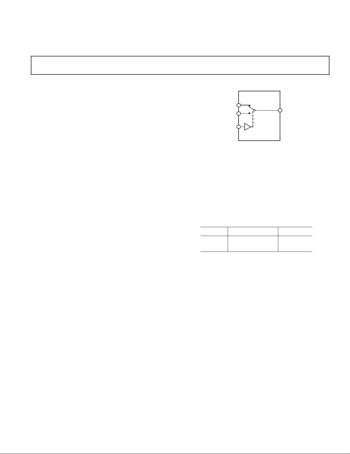
FUNCTIONAL BLOCK DIAGRAM
ADG619/ADG620
S2
S1
IN
SWITCHES SHOWN FOR A LOGIC 1 INPUT
D
GENERAL DESCRIPTION
The ADG619 and the ADG620 are monolithic, CMOS SPDT
(single pole, double throw) switches. Each switch conducts
equally well in both directions when on.
The ADG619/ADG620 offer low on resistance of 4 Ω, which is
matched to within 0.7 Ω between channels. These switches also
provide low power dissipation yet give high switching speeds. The
ADG619 exhibits break-before-make switching action, thus
preventing momentary shorting when switching channels. The
ADG620 exhibits make-before-break action.
The ADG619/ADG620 are available in an 8-lead SOT-23 package and an 8-lead MSOP package.
Table I. Truth Table for the ADG619/ADG620
IN Switch S1 Switch S2
0 ON OFF
1 OFF ON
PRODUCT HIGHLIGHTS
1. Low On Resistance (RON) (4 Ω typ).
2. Dual ± 2.7 V to ± 5.5 V or Single 2.7 V to 5.5 V Supply.
3. Low Power Dissipation. CMOS construction ensures low
power dissipation.
4. Fast t
5.
Tiny 8-Lead SOT-23 Package and 8-Lead
ON/tOFF
.
MSOP P
ackage.
REV. A
Information furnished by Analog Devices is believed to be accurate and
reliable. However, no responsibility is assumed by Analog Devices for its
use, nor for any infringements of patents or other rights of third parties that
may result from its use. No license is granted by implication or otherwise
under any patent or patent rights of Analog Devices. Trademarks and
registered trademarks are the property of their respective companies.
One Technology Way, P.O. Box 9106, Norwood, MA 02062-9106, U.S.A.
Tel: 781/329-4700 www.analog.com
Fax: 781/326-8703 © 2003 Analog Devices, Inc. All rights reserved.

ADG619/ADG620–SPECIFICATIONS
DUAL SUPPLY
1
(V
= +5 V ⴞ 10%, V
DD
= –5 V ⴞ 10%, GND = 0 V. All specifications –40ⴗC to +85ⴗC, unless otherwise noted.)
SS
B Version
Parameter +25ⴗC –40ⴗC to +85ⴗC Unit Test Conditions/Comments
ANALOG SWITCH
Analog Signal Range VSS to V
On Resistance (R
)4 Ω typ VS = ± 4.5 V, IS = –10 mA;
ON
DD
VV
= +4.5 V, VSS = –4.5 V
DD
68 Ω max Test Circuit 1
On Resistance Match between
Channels (∆R
) 0.7 Ω typ VS = ± 4.5 V, IS = –10 mA
ON
1.1 1.35 Ω max
On Resistance Flatness (R
FLAT (ON)
) 0.7 0.8 Ω typ VS = ± 3.3 V, IS = –10 mA
1.15 1.2 Ω max
LEAKAGE CURRENTS V
Source OFF Leakage I
(OFF) ± 0.01 nA typ VS = ± 4.5 V, VD = 4.5 V;
S
= +5.5 V, VSS = –5.5 V
DD
±
± 0.25 ± 1nA max Test Circuit 2
Channel ON Leakage I
, IS (ON) ± 0.01 nA typ VS = VD = ± 4.5 V; Test Circuit 3
D
± 0.25 ± 1nA max
DIGITAL INPUTS
Input High Voltage, V
Input Low Voltage, V
INL
INH
2.4 V min
0.8 V max
Input Current
I
INL
or I
INH
0.005 µA typ VIN = V
INL
or V
INH
± 0.1 µA max
CIN, Digital Input Capacitance 2 pF typ
DYNAMIC CHARACTERISTICS
2
ADG619
t
ON
t
OFF
Break-Before-Make Time Delay, t
80 ns typ RL = 300 Ω, CL = 35 pF
120 155 ns max V
= 3.3 V; Test Circuit 4
S
45 ns typ RL = 300 Ω, CL = 35 pF
75 90 ns max V
40 ns typ RL = 300 Ω, CL = 35 pF
BBM
10 ns min V
= 3.3 V; Test Circuit 4
S
= VS2 = 3.3 V; Test Circuit 5
S1
ADG620
t
ON
t
OFF
Make-Before-Break Time Delay, t
Charge Injection 110 pC typ V
40 ns typ RL = 300 Ω, CL = 35 pF
65 85 ns max V
= 3.3 V; Test Circuit 4
S
200 ns typ RL = 300 Ω, CL = 35 pF
330 400 ns max V
160 ns typ RL = 300 Ω, CL = 35 pF
MBB
10 ns min V
= 3.3 V; Test Circuit 4
S
= 0 V; Test Circuit 6
S
= 0 V, RS = 0 Ω, CL = 1 nF;
S
Test Circuit 7
Off Isolation –67 dB typ R
= 50 Ω, CL = 5 pF, f = 1 MHz;
L
Test Circuit 8
Channel-to-Channel Crosstalk –67 dB typ R
= 50 Ω, CL = 5 pF, f = 1 MHz;
L
Test Circuit 10
Bandwidth –3 dB 190 MHz typ R
C
(OFF) 25 pF typ f = 1 MHz
S
C
(ON) 95 pF typ f = 1 MHz
D, CS
POWER REQUIREMENTS V
I
DD
0.001 µA typ Digital Inputs = 0 V or 5.5 V
= 50 Ω, CL = 5 pF; Test Circuit 9
L
= +5.5 V, VSS = –5.5 V
DD
1.0 µA max
I
SS
0.001 µA typ Digital Inputs = 0 V or 5.5 V
1.0 µA max
NOTES
1
Temperature range is as follows: B Version, –40°C to +85°C.
2
Guaranteed by design, not subject to production test.
Specifications subject to change without notice.
–2–
REV. A

ADG619/ADG620
1
SINGLE SUPPLY
Parameter +25ⴗC –40ⴗC to +85ⴗC Unit Test Conditions/Comments
ANALOG SWITCH
Analog Signal Range 0 V to V
On Resistance (R
On Resistance Match between
Channels (∆R
On Resistance Flatness (R
LEAKAGE CURRENTS V
Source OFF Leakage I
Channel ON Leakage I
DIGITAL INPUTS
Input High Voltage, V
Input Low Voltage, V
Input Current
or I
I
INL
CIN, Digital Input Capacitance 2 pF typ
DYNAMIC CHARACTERISTICS
ADG619
t
ON
t
OFF
Break-Before-Make Time Delay, t
ADG620
t
ON
t
OFF
Make-Before-Break Time Delay, t
Charge Injection 6 pC typ V
Off Isolation –67 dB typ R
Channel-to-Channel Crosstalk –67 dB typ R
Bandwidth –3 dB 190 MHz typ R
(OFF) 25 pF typ f = 1 MHz
C
S
CD, CS (ON) 95 pF typ f = 1 MHz
POWER REQUIREMENTS V
I
DD
NOTES
1
Temperature range is as follows: B Version, –40°C to +85°C.
2
Guaranteed by design, not subject to production test.
Specifications subject to change without notice.
ON
INH
(VDD = +5 V ⴞ 10%, VSS = 0 V, GND = 0 V. All specifications –40ⴗC to +85ⴗC, unless otherwise noted.)
B Version
)7 Ω typ VS = 0 V to 4.5 V, IS = –10 mA;
ON
DD
VV
= 4.5 V, VSS = 0 V
DD
10 12.5 Ω max Test Circuit 1
) 0.8 Ω typ VS = 0 V to 4.5 V, IS = –10 mA
1.1 1.3 Ω max
FLAT (ON)
) 0.5 0.5 Ω typ VS = 1.5 V to 3.3 V, IS = –10 mA
1 Ω max
= 5.5 V
(OFF) ± 0.01 nA typ VS = 1 V/4.5 V, VD = 4.5 V/1 V;
S
DD
± 0.25 ± 1nA max Test Circuit 2
, IS (ON) ± 0.01 nA typ VS = VD = 1 V/4.5 V;
D
± 0.25 ± 1nA max Test Circuit 3
INH
INL
0.005 µA typ VIN = V
2.4 V min
0.8 V max
INL
or V
INH
± 0.1 µA max
2
120 ns typ RL = 300 Ω, CL = 35 pF
220 280 ns max V
= 3.3 V; Test Circuit 4
S
50 ns typ RL = 300 Ω, CL = 35 pF
= 3.3 V; Test Circuit 4
S
= VS2 = 3.3 V; Test Circuit 5
S1
BBM
75 110 ns max V
70 ns typ RL = 300 Ω, CL = 35 pF,
10 ns min V
50 ns typ RL = 300 Ω, CL = 35 pF
85 110 ns max V
= 3.3 V; Test Circuit 4
S
210 ns typ RL = 300 Ω, CL = 35 pF
MBB
340 420 ns max V
170 ns typ RL = 300 Ω, CL = 35 pF
10 ns min V
= 3.3 V; Test Circuit 4
S
= 3.3 V; Test Circuit 6
S
= 0 V, RS = 0 Ω, CL = 1 nF;
S
Test Circuit 7
= 50 Ω, CL = 5 pF, f = 1 MHz;
L
Test Circuit 8
= 50 Ω, CL = 5 pF, f = 1 MHz;
L
Test Circuit 10
= 50 Ω, CL = 5 pF; Test Circuit 9
L
= 5.5 V
DD
0.001 µA typ Digital Inputs = 0 V or 5.5 V
1.0 µA max
REV. A
–3–
 Loading...