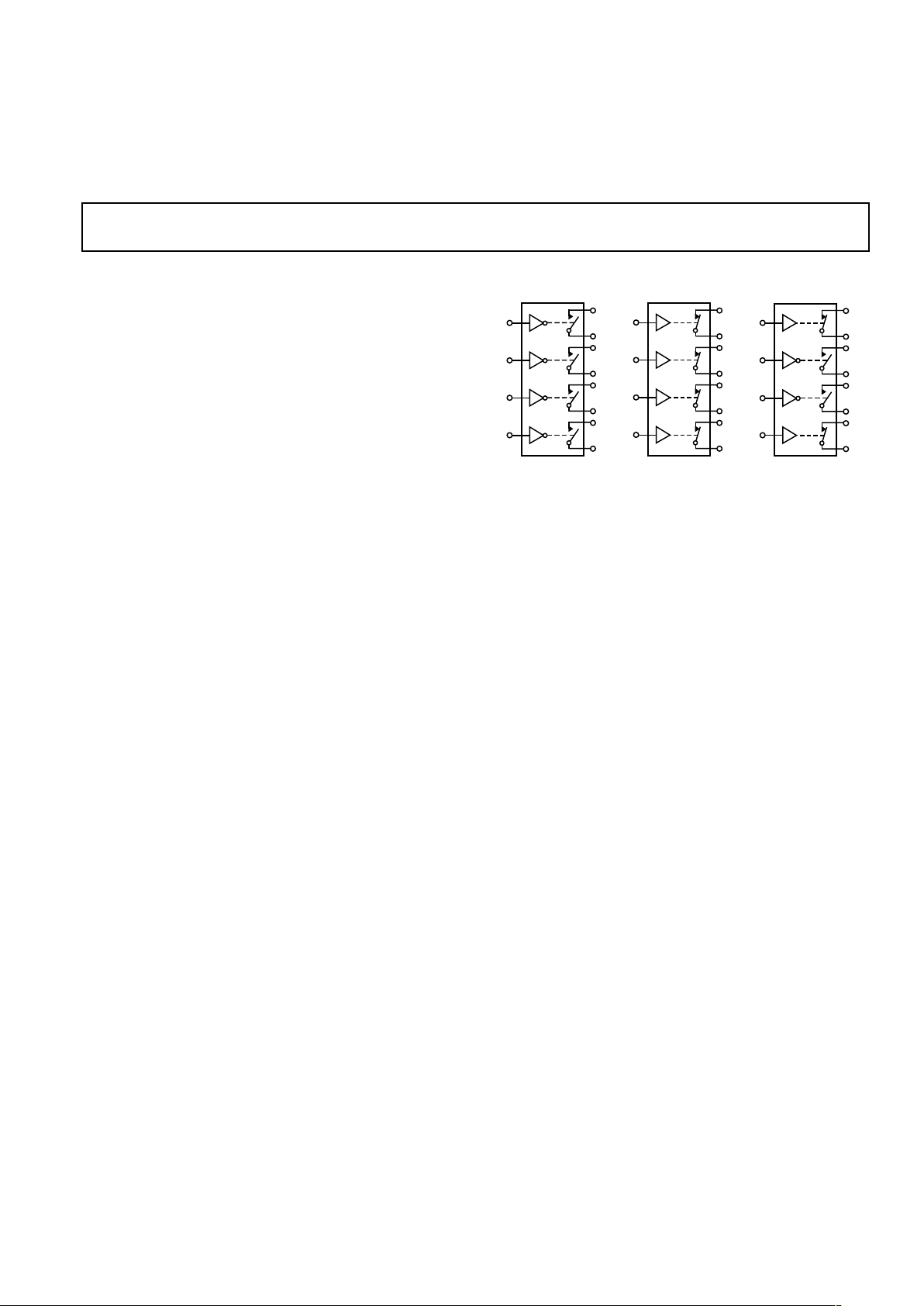
FUNCTIONAL BLOCK DIAGRAMS
IN1
IN2
IN3
IN4
S1
D1
S2
D2
S3
D3
S4
D4
ADG511
IN1
IN2
IN3
IN4
S1
D1
S2
D2
S3
D3
S4
D4
ADG512
IN1
IN2
IN3
IN4
S1
D1
S2
D2
S3
D3
S4
D4
ADG513
SWITCHES SHOWN FOR A LOGIC "1" INPUT
REV. C
Information furnished by Analog Devices is believed to be accurate and
reliable. However, no responsibility is assumed by Analog Devices for its
use, nor for any infringements of patents or other rights of third parties that
may result from its use. No license is granted by implication or otherwise
under any patent or patent rights of Analog Devices.
a
LC2MOS
Precision 5 V/3 V Quad SPST Switches
ADG511/ADG512/ADG513
FEATURES
+3 V, +5 V or 5 V Power Supplies
Ultralow Power Dissipation (<0.5 W)
Low Leakage (<100 pA)
Low On Resistance (<50 )
Fast Switching Times
Low Charge Injection
TTL/CMOS Compatible
16-Lead DIP or SOIC Package
APPLICATIONS
Battery-Powered Instruments
Single Supply Systems
Remote Powered Equipment
5 V Supply Systems
Computer Peripherals such as Disk Drives
Precision Instrumentation
Audio and Video Switching
Automatic Test Equipment
Precision Data Acquisition
Sample Hold Systems
Communication Systems
Compatible with 5 V Supply DACs and ADCs such as
AD7840/AD7848, AD7870/AD7871/AD7872/AD7874/
AD7875/AD7876/AD7878
GENERAL DESCRIPTION
The ADG511, ADG512 and ADG513 are monolithic CMOS
ICs containing four independently selectable analog switches.
These switches feature low, well-controlled on resistance and
wide analog signal range, making them ideal for precision
analog signal switching.
These switch arrays are fabricated using Analog Devices’
advanced linear compatible CMOS (LC
2
MOS) process which
offers the additional benefits of low leakage currents, ultralow
power dissipation and low capacitance for fast switching speeds
with minimum charge injection. These features make the
ADG511, ADG512 and ADG513 the optimum choice for a
wide variety of signal switching tasks in precision analog signal
processing and data acquisition systems.
The ability to operate from single +3 V, +5 V or ±5 V bipolar
supplies make the ADG511, ADG512 and ADG513 perfect for
use in battery-operated instruments, 4–20 mA loop systems and
with the new generation of DACs and ADCs from Analog
Devices. The use of 5 V supplies and reduced operating currents
give much lower power dissipation than devices operating from
± 15 V supplies.
The ADG511, ADG512 and ADG513 contain four independent SPST switches. The ADG511 and ADG512 differ only in
that the digital control logic is inverted. The ADG511 switch is
turned on with a logic low on the appropriate control input,
while a logic high is required for the ADG512. The ADG513
contains two switches whose digital control logic is similar to
that of the ADG511 while the logic is inverted in the remaining
two switches.
PRODUCT HIGHLIGHTS
1. 5 Volt Single Supply Operation
The ADG511/ADG512/ADG513 offers high performance,
including low on resistance and wide signal range, fully
specified and guaranteed with +3 V, ±5 V as well as +5 V
supply rails.
2. Ultralow Power Dissipation
CMOS construction ensures ultralow power dissipation.
3. Low R
ON
4. Break-Before-Make Switching
Switches are guaranteed to have break-before-make operation. This allows multiple outputs to be tied together for
multiplexer applications without the possibility of momentary
shorting between channels.
One Technology Way, P.O. Box 9106, Norwood, MA 02062-9106, U.S.A.
Tel: 781/329-4700 www.analog.com
Fax: 781/326-8703 © Analog Devices, Inc., 2001

Dual Supply
B Versions T Version
–40C to –55C to
Parameter 25C +85C25C +125C Unit Test Conditions/Comments
ANALOG SWITCH
Analog Signal Range V
DD
to V
SS
VDD to VSSV
R
ON
30 30 Ω typ VD = ± 3.5 V, IS = –10 mA;
50 50 Ω max VDD = +4.5 V, VSS = –4.5 V
LEAKAGE CURRENTS VDD = +5.5 V, VSS = –5.5 V
Source OFF Leakage I
S
(OFF) ± 0.025 ± 0.025 nA typ VD = ± 4.5 V, VS = ⫿4.5 V;
± 0.1 ± 2.5 ± 0.1 ± 2.5 nA max Test Circuit 2
Drain OFF Leakage I
D
(OFF) ± 0.025 ± 0.025 nA typ VD = ± 4.5 V, VS = ⫿4.5 V;
± 0.1 ± 2.5 ± 0.1 ± 2.5 nA max Test Circuit 2
Channel ON Leakage I
D
, IS (ON) ± 0.05 ± 0.05 nA typ VD = VS = ± 4.5 V;
± 0.2 ± 5 ± 0.2 ± 5 nA max Test Circuit 3
DIGITAL INPUTS
Input High Voltage, V
INH
2.4 2.4 V min
Input Low Voltage, V
INL
0.8 0.8 V max
Input Current
I
INL
or I
INH
0.005 0.005 µA typ VIN = V
INL
or V
INH
± 0.1 ± 0.1 µA max
DYNAMIC CHARACTERISTICS
2
t
ON
200 200 ns typ RL = 300 Ω. CL = 35 pF;
375 375 ns max V
S
= ± 3 V; Test Circuit 4
t
OFF
120 120 ns typ RL = 300 Ω. CL = 35 pF;
150 150 ns max V
S
= ± 3 V; Test Circuit 4
Break-Before-Make Time 100 100 ns typ R
L
= 300 Ω, CL = 35 pF;
Delay, t
D
(ADG513 Only) VS1 = VS2 = 3 V; Test Circuit 5
Charge Injection 11 11 pC typ V
S
= 0 V, RS = 0 Ω, CL = 10 nF;
Test Circuit 6
OFF Isolation 68 68 dB typ R
L
= 50 Ω, CL = 5 pF, f = 1 MHz;
Test Circuit 7
Channel-to-Channel Crosstalk 85 85 dB typ R
L
= 50 Ω, CL = 5 pF, f = 1 MHz;
Test Circuit 8
C
S
(OFF) 9 9 pF typ f = 1 MHz
C
D
(OFF) 9 9 pF typ f = 1 MHz
CD, CS (ON) 35 35 pF typ f = 1 MHz
POWER REQUIREMENTS
V
DD
+4.5/5.5 +4.5/5.5 V min/max
V
SS
–4.5/–5.5 –4.5/–5.5 V min/max
I
DD
0.0001 0.0001 µA typ VDD = +5.5 V, VSS = –5.5 V
11µA max Digital Inputs = 0 V or 5 V
I
SS
0.0001 0.0001 µA typ
11µA max
NOTES
1
Temperature ranges are as follows: B Versions –40°C to +85°C; T Version –55°C to +125°C.
2
Guaranteed by design, not subject to production test.
Specifications subject to change without notice.
REV. C–2–
(VDD = +5 V 10%, VSS = –5 V 10%, GND = 0 V, unless otherwise noted)
ADG511/ADG512/ADG513–SPECIFICATIONS
1

Single Supply
B Versions T Version
–40C to –55C to
Parameter 25C +85C25C +125C Unit Test Conditions/Comments
ANALOG SWITCH
Analog Signal Range 0 V to V
DD
0 V to VDDV
R
ON
45 45 Ω typ VD = 3.5 V, IS = –10 mA;
75 75 Ω max VDD = 4.5 V
LEAKAGE CURRENTS V
DD
= 5.5 V
Source OFF Leakage I
S
(OFF) ± 0.025 ± 0.025 nA typ VD = 4.5/1 V, VS = 1Ⲑ4.5 V;
± 0.1 ±2.5 ± 0.1 ± 2.5 nA max Test Circuit 2
Drain OFF Leakage I
D
(OFF) ± 0.025 ± 0.025 nA typ VD = 4.5/1 V, VS = 1Ⲑ4.5 V;
± 0.1 ±2.5 ± 0.1 ± 2.5 nA max Test Circuit 2
Channel ON Leakage I
D
, IS (ON) ± 0.05 ± 0.05 nA typ VD = VS = 4.5 V/1 V;
± 0.2 ±5 ± 0.2 ± 5 nA max Test Circuit 3
DIGITAL INPUTS
Input High Voltage, V
INH
2.4 2.4 V min
Input Low Voltage, V
INL
0.8 0.8 V max
Input Current
I
INL
or I
INH
0.005 0.005 µA typ VIN = V
INL
or V
INH
± 0.1 ±0.1 µA max
DYNAMIC CHARACTERISTICS
2
t
ON
250 250 ns typ RL = 300 Ω, CL = 35 pF;
500 500 ns max V
S
= 2 V; Test Circuit 4
t
OFF
50 50 ns typ RL = 300 Ω, CL = 35 pF;
100 100 ns max V
S
= 2 V; Test Circuit 4
Break-Before-Make Time 200 200 ns typ R
L
= 300 Ω, CL = 35 pF;
Delay, t
D
(ADG513 Only) VS1 = VS2 = 2 V; Test Circuit 5
Charge Injection 16 16 pC typ V
S
= 0 V, RS = 0 Ω, CL = 10 nF;
Test Circuit 6
OFF Isolation 68 68 dB typ R
L
= 50 Ω, CL = 5 pF, f = 1 MHz;
Test Circuit 7
Channel-to-Channel Crosstalk 85 85 dB typ R
L
= 50 Ω, CL = 5 pF, f = 1 MHz;
Test Circuit 8
C
S
(OFF) 9 9 pF typ f = 1 MHz
C
D
(OFF) 9 9 pF typ f = 1 MHz
CD, CS (ON) 35 35 pF typ f = 1 MHz
POWER REQUIREMENTS
V
DD
4.5/5.5 4.5/5.5 V min/max
I
DD
0.0001 0.0001 µA typ VDD = 5.5 V
11µA max Digital Inputs = 0 V or 5 V
NOTES
1
Temperature ranges are as follows: B Versions –40°C to +85°C; T Version –55°C to +125°C.
2
Guaranteed by design, not subject to production test.
Specifications subject to change without notice.
(VDD = 5 V 10%, VSS = 0 V, GND = 0 V, unless otherwise noted)
ADG511/ADG512/ADG513
REV. C
–3–

Single Supply
B Version
0C to
Parameter 25C70C Unit Test Conditions/Comments
ANALOG SWITCH
Analog Signal Range 0 V to V
DD
V
R
ON
200 Ω typ VD = 1.5 V, IS = –1 mA;
500 Ω max VDD = 3 V
LEAKAGE CURRENTS V
DD
= 3.6 V
Source OFF Leakage I
S
(OFF) ± 0.025 nA typ VD = 2.6/1 V, VS = 1Ⲑ2.6 V;
± 0.1 ± 2.5 nA max Test Circuit 2
Drain OFF Leakage I
D
(OFF) ± 0.025 nA typ VD = 2.6/1 V, VS = 1Ⲑ2.6 V;
± 0.1 ± 2.5 nA max Test Circuit 2
Channel ON Leakage I
D
, IS (ON) ±0.05 nA typ VD = VS = 2.6 V/1 V;
± 0.2 ± 5 nA max Test Circuit 3
DIGITAL INPUTS
Input High Voltage, V
INH
2.4 V min
Input Low Voltage, V
INL
0.8 V max
Input Current
I
INL
or I
INH
0.005 µA typ VIN = V
INL
or V
INH
± 0.1 µA max
DYNAMIC CHARACTERISTICS
2
t
ON
600 ns typ RL = 300 Ω, CL = 35 pF;
1200 ns max V
S
= 1 V; Test Circuit 4
t
OFF
100 ns typ RL = 300 Ω, CL = 35 pF;
160 ns max V
S
= 1 V; Test Circuit 4
Break-Before-Make Time 500 ns typ R
L
= 300 Ω, CL = 35 pF;
Delay, t
D
(ADG513 Only) VS1 = VS2 = 1 V; Test Circuit 5
Charge Injection 11 pC typ V
S
= 0 V, RS = 0 Ω, CL = 10 nF;
Test Circuit 6
OFF Isolation 68 dB typ R
L
= 50 Ω, CL = 5 pF, f = 1 MHz;
Test Circuit 7
Channel-to-Channel Crosstalk 85 dB typ R
L
= 50 Ω, CL = 5 pF, f = 1 MHz;
Test Circuit 8
C
S
(OFF) 9 pF typ f = 1 MHz
C
D
(OFF) 9 pF typ f = 1 MHz
CD, CS (ON) 35 pF typ f = 1 MHz
POWER REQUIREMENTS
V
DD
3/3.6 V min/max
I
DD
0.0001 µA typ VDD = 3.6 V
1 µA max Digital Inputs = 0 V or 3 V
NOTES
1
Temperature range is as follows: B Version –40°C to +85°C.
2
Guaranteed by design, not subject to production test.
Specifications subject to change without notice.
REV. C
–4–
ADG511/ADG512/ADG513–SPECIFICATIONS
1
(VDD = 3.3 V 10%, VSS = 0 V, GND = 0 V, unless otherwise noted)
