

8-Channel/4-Channel
Fault-Protected Analog Multiplexers
FEATURES
All switches off with power supply off
Analog output of on channel clamped within power
supplies if an overvoltage occurs
Latch-up proof construction
Low on resistance (270 Ω typical)
Fast switching times
t
: 230 ns maximum
ON
t
: 130 ns maximum
OFF
Low power dissipation (3.3 mW maximum)
Fault and overvoltage protection (−40 V to +55 V)
Break-before-make construction
TTL and CMOS compatible inputs
APPLICATIONS
Existing multiplexer applications (both fault-protected and
nonfault-protected)
New designs requiring multiplexer functions
GENERAL DESCRIPTION
The ADG508F and ADG509F are CMOS analog multiplexers, with the ADG508F comprising eight single channels
and the ADG509F comprising four differential channels. These
multiplexers provide fault protection. Using a series n-channel,
p-channel, n-channel MOSFET structure, both device and signal
source protection is provided in the event of an overvoltage or
power loss. The multiplexer can withstand continuous overvoltage inputs from −40 V to +55 V. During fault conditions with
power supplies off, the multiplexer input (or output) appears as
an open circuit and only a few nanoamperes of leakage current
will flow. This protects not only the multiplexer and the circuitry
driven by the multiplexer, but also protects the sensors or signal
sources that drive the multiplexer.
The ADG508F switches one of eight inputs to a common output
as determined by the 3-bit binary address lines A0, A1, and A2.
The ADG509F switches one of four differential inputs to a
common differential output as determined by the 2-bit binary
address lines A0 and A1. An EN input on each device is used
to enable or disable the device. When disabled, all channels are
switched off.
Rev. F
Information furnished by Analog Devices is believed to be accurate and reliable. However, no
responsibility is assumed by Anal og Devices for its use, nor for any infringements of patents or ot her
rights of third parties that may result from its use. Specifications subject to change without notice. No
license is granted by implication or otherwise under any patent or patent rights of Analog Devices.
Trademarks and registered trademarks are the property of their respective owners.
ADG508F/ADG509F
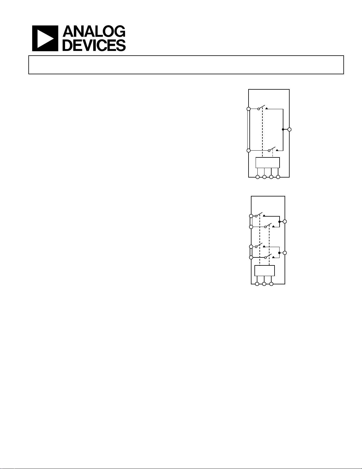
FUNCTIONAL BLOCK DIAGRAMS
ADG508F
S1
D
S8
1 OF 8
DECODER
A0
A1 A2 EN
Figure 1.
ADG509F
S1A
S4A
S1B
S4B
1 OF 4
DECODER
A1
A0
EN
Figure 2.
PRODUCT HIGHLIGHTS
1. Fault protection. The ADG508F/ADG509F can withstand
continuous voltage inputs from −40 V to +55 V. When a
fault occurs due to the power supplies being turned off, all
the channels are turned off and only a leakage current of a
few nanoamperes flows.
2. On channel saturates while fault exists.
3. Low R
4. Fast switching times.
5. Break-before-make switching. Switches are guaranteed
break-before-make so that input signals are protected
against momentary shorting.
6. Trench isolation eliminates latch-up. A dielectric trench
separates the p and n-channel MOSFETs thereby
preventing latch-up.
One Technology Way, P.O. Box 9106, Norwood, MA 02062-9106, U.S.A.
Tel: 781.329.4700 www.analog.com
Fax: 781.461.3113 ©2001–2011 Analog Devices, Inc. All rights reserved.
ON
.
DA
DB
00035-001
00035-101

ADG508F/ADG509F
TABLE OF CONTENTS
Features.............................................................................................. 1
Applications....................................................................................... 1
General Description ......................................................................... 1
Functional Block Diagrams............................................................. 1
Product Highlights ........................................................................... 1
Revision History ............................................................................... 2
Specifications..................................................................................... 3
Dual Supply................................................................................... 3
Truth Tables................................................................................... 4
REVISION HISTORY
7/11—Rev. E to Rev. F
Deleted ADG528F ..............................................................Universal
Changes to Features Section and General Description Section . 1
Changes to Specifications Section.................................................. 3
Deleted Timing Diagrams Section................................................. 4
Changes to Table 4............................................................................ 5
Added Table 5.................................................................................... 6
Added Table 6.................................................................................... 7
Replaced Typical Performance Characteristics Section .............. 8
Changes to Terminology Section.................................................. 10
Changes to Figure 27 and Figure 28............................................. 13
Changes to Figure 31...................................................................... 14
Changes to Theory of Operation Section.................................... 11
Updated Outline Dimensions....................................................... 15
Changes to Ordering Guide.......................................................... 17
7/09—Rev. D: Rev. E
Updated Format..................................................................Universal
Added TSSOP .....................................................................Universal
Updated Outline Dimensions....................................................... 15
Changes to Ordering Guide.......................................................... 18
4/01—Data Sheet Changed from Rev. C to Rev. D.
Changes to Ordering Guide............................................................ 1
Changes to Specifications Table...................................................... 2
Max Ratings Changed...................................................................... 4
Deleted 16-Lead Cerdip from Outline Dimensions ..................11
Deleted 18-Lead Cerdip from Outline Dimensions ..................12
Absolute Maximum Ratings ............................................................5
ESD Caution...................................................................................5
Pin Configuration and Function Descriptions..............................6
Typical Performance Characteristics..............................................8
Terminology.................................................................................... 10
Theory of Operation ...................................................................... 11
Test Circuits..................................................................................... 12
Outline Dimensions....................................................................... 15
Ordering Guide .......................................................................... 17
Rev. F | Page 2 of 20

ADG508F/ADG509F
SPECIFICATIONS
DUAL SUPPLY
VDD = +15 V ± 10%, VSS = −15 V ± 10%, GND = 0 V, unless otherwise noted.
Table 1.
B Version
Parameter +25°C −40°C to +85°C Unit Test Conditions/Comments
ANALOG SWITCH
Analog Signal Range VSS + 1.4 V typ Output open circuit
V
V
V
RON 270 350 Ω typ −10 V ≤ VS ≤ +10 V, IS = 1 mA;
390 Ω max
RON Drift 0.6 %/°C typ VS = 0 V, IS = 1 mA
On-Resistance Match Between
Channels, R
ON
LEAKAGE CURRENTS
Source Off Leakage IS (Off) ±0.02 nA typ
±1 ±50 nA max See Figure 22
Drain Off Leakage ID (Off)
ADG508F ±1 ±60 nA max See Figure 23
ADG509F ±1 ±30 nA max
Channel On Leakage ID, IS (On) ±0.04 nA typ VS = VD = ± 10 V;
ADG508F ±1 ±60 nA max See Figure 24
ADG509F ±1 ±30 nA max
FAU LT
Source Leakage Current IS (Fault) ±0.02 nA typ VS = +55 V or −40 V, VD = 0 V, see Figure 25
(With Overvoltage) ±2 ±2 A max
Drain Leakage Current ID (Fault)
(With Overvoltage) ±2 A max
Source Leakage Current IS (Fault)
(Power Supplies Off)
±2 A max See Figure 26
DIGITAL INPUTS
Input High Voltage, V
Input Low Voltage, V
Input Current, I
INL
2.4 V min
INH
0.8 V max
INL
or I
±1 A max VIN = 0 or VDD
INH
CIN, Digital Input Capacitance 5 pF typ
DYNAMIC CHARACTERISTICS1
t
175 ns typ RL = 1 MΩ, CL = 35 pF;
TRANSITION
t
90 ns typ RL = 1 kΩ, CL = 35 pF;
OPEN
60 40 ns min VS = 5 V; see Figure 28
tON (EN) 180 ns typ RL = 1 kΩ, CL = 35 pF;
230 300 ns max VS = 5 V; see Figure 29
t
(EN) 100 ns typ RL = 1 kΩ, CL = 35 pF
OFF
130 150
t
, Settling Time ns max VS = 5 V; see Figure 29
SETT
0.1% 1 s typ RL = 1 kΩ, CL = 35 pF;
0.01% 2.5 s typ VS = 5 V
− 1.4 V typ
DD
+ 2.2 V typ Output loaded, 1 mA
SS
– 2.2 V typ
DD
= +15 V ± 10%, VSS = −15 V ± 10%
V
DD
See Figure 21
3 % max V
±0.04 nA typ
±5 nA typ
±1 nA typ V
220 300 ns max
= ±10 V, IS = −1 mA
S
= ±10 V, VS = +10 V;
V
D
V
= ±10 V, VS = +10 V;
D
V
= ±25 V, VD = +10 V, see Figure 23
S
= ±25 V, VD = VEN = A0, A1, A2 = 0 V
S
V
= ±10 V, VS8 = +10 V; see Figure 27
S1
Rev. F | Page 3 of 20
ADG508F/ADG509F
B Version
Parameter +25°C −40°C to +85°C Unit Test Conditions/Comments
Charge Injection 15 pC typ VS = 0 V, RS = 0 Ω, CL= 1 nF; see Figure 30
Off Isolation 93 dB typ
CS (Off) 3 pF typ
CD (Off)
ADG508F 22 pF typ
ADG509F 12 pF typ
POWER REQUIREMENTS
IDD 0.05 0.2 mA max VIN = 0 V or 5 V
ISS 0.1 1 µA max
1
Guaranteed by design, not subject to production test.
TRUTH TABLES
Table 2. ADG508F Truth Table1
A2 A1 A0 EN On Switch
X X X 0 None
0 0 0 1 1
0 0 1 1 2
0 1 0 1 3
0 1 1 1 4
1 0 0 1 5
1 0 1 1 6
1 1 0 1 7
1 1 1 1 8
1
X = don’t care.
= 1 kΩ, CL = 15 pF, f = 100 kHz; VS = 7 V rms;
R
L
see Figure 31
Table 3. ADG509F Truth Table1
A1 A0 EN On Switch Pair
X X 0 None
0 0 1 1
0 1 1 2
1 0 1 3
1 1 1 4
1
X = don’t care.
Rev. F | Page 4 of 20
ADG508F/ADG509F
ABSOLUTE MAXIMUM RATINGS
TA = 25°C unless otherwise noted.
Table 4.
Parameter Rating
VDD to VSS 48 V
VDD to GND −0.3 V to +48 V
VSS to GND +0.3 V to −48 V
Digital Input, EN, Ax −0.3 V to VDD + 0.3 V or
VS, Analog Input Overvoltage with
Power On (V
VS, Analog Input Overvoltage with
Power Off (V
Continuous Current, S or D 20 mA
Peak Current, S or D
(Pulsed at 1 ms, 10% Duty Cycle Max) 40 mA
Operating Temperature Range
Industrial (B Version) −40°C to +85°C
Storage Temperature Range −65°C to +150°C
Junction Temperature 150°C
TSSOP
θJA, Thermal Impedance 112°C/W
Plastic DIP Package
θJA, Thermal Impedance
16-Lead 117°C/W
SOIC Package
θJA, Thermal Impedance
Narrow Body 77°C/W
Wide Body 75°C/W
= +15 V, VSS = −15 V)
DD
= 0 V, VSS = 0 V)
DD
20 mA, whichever occurs first
V
− 25 V to VDD + 40 V
SS
−40 V to +55 V
Stresses above those listed under Absolute Maximum Ratings
may cause permanent damage to the device. This is a stress
rating only; functional operation of the device at these or any
other conditions above those indicated in the operational
section of this specification is not implied. Exposure to absolute
maximum rating conditions for extended periods may affect
device reliability.
ESD CAUTION
Rev. F | Page 5 of 20
ADG508F/ADG509F
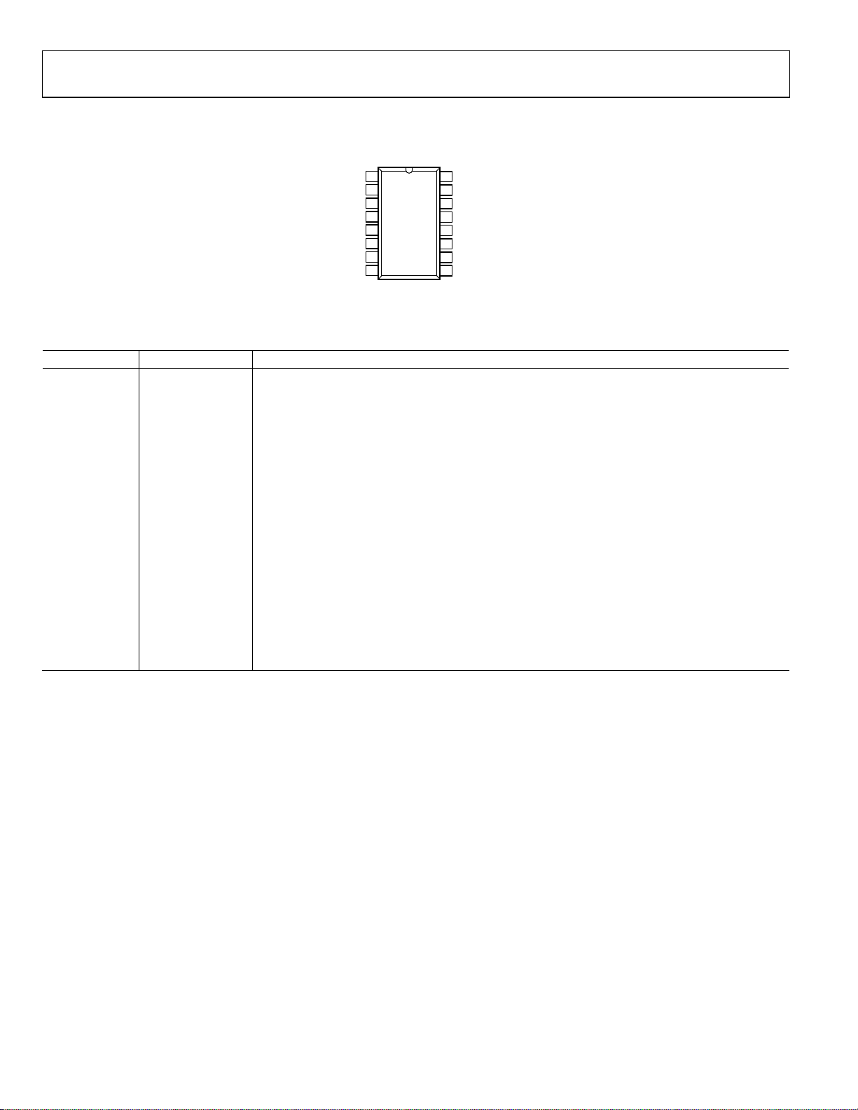
PIN CONFIGURATION AND FUNCTION DESCRIPTIONS
1
A0
2
EN
V
3
SS
ADG508F
TOP VIEW
S1
4
(Not to Scale)
S2
5
S3
6
7
S4
8
D
Figure 3. ADG508F Pin Configuration
Table 5. ADG508F Pin Function Descriptions
Pin No. Mnemonic Description
1 A0 Logic Control Input.
2 EN
Active High Digital Input. When low, the device is disabled and all switches are off. When high,
Ax logic inputs determine on switches.
3 VSS
Most Negative Power Supply Potential. In single-supply applications, this pin can be connected
to ground.
4 S1 Source Terminal 1. This pin can be an input or an output.
5 S2 Source Terminal 2. This pin can be an input or an output.
6 S3 Source Terminal 3. This pin can be an input or an output.
7 S4 Source Terminal 4. This pin can be an input or an output.
8 D Drain Terminal. This pin can be an input or an output.
9 S8 Source Terminal 8. This pin can be an input or an output.
10 S7 Source Terminal 7. This pin can be an input or an output.
11 S6 Source Terminal 6. This pin can be an input or an output.
12 S5 Source Terminal 5. This pin can be an input or an output.
13 VDD Most Positive Power Supply Potential.
14 GND Ground (0 V) Reference.
15 A2 Logic Control Input.
16 A1 Logic Control Input.
A1
16
A2
15
GND
14
13
V
DD
12
S5
11
S6
S7
10
S8
9
00035-004
Rev. F | Page 6 of 20

ADG508F/ADG509F
1
A0
2
EN
V
3
SS
ADG509F
DA
TOP VIEW
4
(Not to Scale)
5
6
7
8
S1A
S2A
S3A
S4A
Figure 4. ADG509F Pin Configuration
Table 6. ADG509F Pin Function Descriptions
Pin No. Mnemonic Description
1 A0 Logic Control Input.
2 EN
Active High Digital Input. When low, the device is disabled and all switches are off. When high,
Ax logic inputs determine on switches.
3 VSS
Most Negative Power Supply Potential. In single-supply applications, this pin can be connected
to ground.
4 S1A Source Terminal 1A. This pin can be an input or an output.
5 S2A Source Terminal 2A. This pin can be an input or an output.
6 S3A Source Terminal 3A. This pin can be an input or an output.
7 S4A Source Terminal 4A. This pin can be an input or an output.
8 DA Drain Terminal A. This pin can be an input or an output.
9 DB Drain Terminal B. This pin can be an input or an output.
10 S4B Source Terminal 4B. This pin can be an input or an output.
11 S3B Source Terminal 3B. This pin can be an input or an output.
12 S2B Source Terminal 2B. This pin can be an input or an output.
13 S1B Source Terminal 1B. This pin can be an input or an output.
14 VDD Most Positive Power Supply Potential.
15 GND Ground (0 V) Reference.
16 A1 Logic Control Input.
A1
16
GND
15
V
14
DD
13
S1B
12
S2B
11
S3B
S4B
10
DB
9
00035-005
Rev. F | Page 7 of 20

ADG508F/ADG509F
TYPICAL PERFORMANCE CHARACTERISTICS
2000
1750
1500
1250
(Ω)
1000
ON
R
750
500
TA = 25°C
VDD = +5V
VSS = –5V
V
= +10V
DD
V
= –10V
SS
V
= +15V
DD
V
= –15V
SS
2000
1750
1500
1250
(Ω)
1000
ON
R
750
500
TA = 125°C
T
= 105°C
A
T
= 85°C
A
T
= 25°C
A
VDD = +15V
V
= –15V
SS
250
0
V
, VS(V)
D
Figure 5. On Resistance as a Function of V
1m
100µ
10µ
1µ
100n
10n
1n
INPUT LEAKAGE (A)
S
I
100p
10p
1p
–40
–50 –30 –20 –10 0 10 20 30 40 50 60
OPERATING RANGE
V
SOURCE VOLTAGE (V)
S
V
DD
V
SS
V
= 0V
D
Figure 6. Source Input Leakage Current as a Function of V
Off) During Overvoltage Conditions
250
00035-008
15–15 –10 –5 0 5 10
(VS) Figure 8. On Resistance as a Function of VD (VS) for Different Temperatures
D
= 0V
= 0V
00035-009
(Power Supplies
S
Figure 9. Source Input Leakage Current as a Function of V
0
V
, VS(V)
D
1m
100µ
10µ
1µ
100n
10n
1n
INPUT LEAKAGE (A)
S
I
100p
10p
1p
–40
–50 –30 –20 –10 0 10 20 30 40 50 60
OPERATING RANGE
V
SOURCE VOLT AGE (V)
S
V
= +15V
DD
V
= –15V
SS
V
= 0V
D
(Power Supplies
S
00035-011
15–15 –10 –5 0 5 10
On) During Overvoltage Conditions
00035-012
1m
100µ
10µ
1µ
100n
10n
1n
INPUT LEAKAG E (A)
D
I
100p
10p
1p
–40
–50 –30 –20 –10 0 10 20 30 40 50 60
OPERATING RANGE
V
SOURCE VOLTAGE (V)
S
V
V
V
DD
SS
D
= 0V
= +15V
= –15V
Figure 7. Drain Output Leakage Current as a Function of V
On) During Overvoltage Conditions
00035-010
(Power Supplies
S
Rev. F | Page 8 of 20
0.3
VDD = +15V
= –15V
V
0.2
0.1
0.0
–0.1
LEAKAGE CURRENTS ( nA)
–0.2
–0.3
SS
(VD) = ±10V
V
S
= 25°C
T
A
ID(OFF)
IS(OFF)
ID, IS(ON)
–14 –10 –6 –2 2 6 10 14
Figure 10. Leakage Currents as a Function of V
V
S,VD
(V)
D
00035-013
(VS)

ADG508F/ADG509F
A
TION (dB)
OFF ISOL
–20
–40
–60
–80
–100
0
TA = 25°C
V
= +15V
DD
V
= –15V
SS
100
VDD = +15V
= –15V
V
SS
= +10V
V
D
10
0.1
LEAKAGE CURRENTS (nA)
= –10V
V
S
1
ID(ON)
ID(OFF)
IS(OFF)
0.01
45 5525 65 75 85 95 10535
TEMPERATURE (°C)
Figure 11. Leakage Currents as a Function of Temperature
260
240
220
200
180
160
SWITCHING TIME (ns)
140
120
100
t
10 11 12 13 14 15
t
TRANSITI ON
(EN)
ON
t
(EN)
OFF
POWER SUPPLY (V)
Figure 12. Switching Time vs. Dual Power Supply
300
VDD = +15V
V
= –15V
250
SS
t
(EN)
ON
115 125
00035-014
–120
10k 100k 1M 10M 100M 1G1k
FREQUENCY ( Hz)
000354-113
Figure 14. Off Isolation vs. Frequency, ±15 V Dual Supply
40
TA = 25°C
V
V
DD
SS
= +15V
= –15V
DRAIN OFF
SOURCE OFF
VS (V)
00035-114
35
30
25
20
15
PIN CAPACITANCE (pF)
10
5
00035-015
0
–15 –10 –5 0 5 10 15
Figure 15. Capacitance vs. Source Voltage
30
VDD = +15V
V
= –15V
SS
T
= 25°C
20
A
200
150
100
SWITCHING TIME (ns)
50
0
–40 –20 0 20 40 60 80 100 120
TEMPERATURE (° C)
t
TRANSITI ON
t
Figure 13. Switching Time vs. Temperature
OFF
(EN)
00035-016
10
(pC)
0
INJ
Q
–10
–20
–30
–15 –10 –5 0 5 10 15
VS (V)
Figure 16. Charge Injection vs. Source Voltage
00035-115
Rev. F | Page 9 of 20

ADG508F/ADG509F
TERMINOLOGY
C
(Off)
VDD
Most positive power supply potential.
V
SS
Most negative power supply potential.
GND
Ground (0 V) reference.
R
ON
Ohmic resistance between D and S.
R
Drift
ON
Percentage change in R
when temperature changes by one
ON
degree Celsius.
ΔR
ON
ΔR
represents the difference between the RON of any two
ON
channels as a percentage of the maximum R
of those two
ON
channels.
I
(Off)
S
Source leakage current when the switch is off.
I
(Off)
D
Drain leakage current when the switch is off.
I
, IS (On)
D
Channel leakage current when the switch is on.
I
(Fault—Power Supplies On)
S
Source leakage current when exposed to an overvoltage
condition.
(Fault—Power Supplies On)
I
D
Drain leakage current when exposed to an overvoltage
condition.
I
(Fault—Power Supplies Off)
S
Source leakage current with power supplies off.
V
(VS)
D
Analog Voltage on Terminals D, S.
C
(Off)
S
Channel input capacitance for off condition.
D
Channel output capacitance for off condition.
C
IN
Digital input capacitance.
t
(EN)
ON
Delay time between the 50% and 90% points of the digital input
and switch on condition.
t
(EN)
OFF
Delay time between the 50% and 90% points of the digital input
and switch off condition.
t
TRANSITION
Delay time between the 50% and 90% points of the digital
inputs and the switch on condition when switching from
one address state to another.
t
OPEN
Off time measured between 80% points of both switches when
switching from one address state to another.
V
INL
Maximum input voltage for Logic 0.
V
INH
Minimum input voltage for Logic 1.
I
(I
)
INL
INH
Input current of the digital input.
Off Isolation
A measure of unwanted signal coupling through an off channel.
Charge Injection
A measure of the glitch impulse transferred from the digital
input to the analog output during switching.
I
DD
Positive supply current.
I
SS
Negative supply current.
Rev. F | Page 10 of 20

ADG508F/ADG509F
THEORY OF OPERATION
The ADG508F/ADG509F multiplexers are capable of withstanding overvoltages from −40 V to +55 V, irrespective of whether the
power supplies are present or not. Each channel of the multiplexer
consists of an n-channel MOSFET, a p-channel MOSFET, and an
n-channel MOSFET, connected in series. When the analog input
exceeds the power supplies, one of the MOSFETs will saturate
limiting the current. The current during a fault condition is
determined by the load on the output. Figure 17 illustrates
the channel architecture that enables these multiplexers to
withstand continuous overvoltages.
When an analog input of V
+ 2.2 V to VDD − 2.2 V (output
SS
loaded, 1 mA) is applied to the ADG508F/ADG509F, the
multiplexer behaves as a standard multiplexer, with specifications similar to a standard multiplexer, for example,
the on-resistance is 390 Ω maximum. However, when an
overvoltage is applied to the device, one of the three
MOSFETs saturate.
Figure 17 to Figure 20 show the conditions of the three MOSFETs
for the various overvoltage situations. When the analog input
applied to an on channel approaches the positive power supply
line, the n-channel MOSFET saturates because the voltage on
the analog input exceeds the difference between V
n-channel threshold voltage (V
tive than V
is applied to the multiplexer, the p-channel
SS
). When a voltage more nega-
TN
and the
DD
MOSFET will saturate because the analog input is more
negative than the difference between V
threshold voltage (V
V
−1.4 V, the analog input range to the multiplexer is limited
TP
to V
+ 1.4 V to VDD – 1.4 V (output open circuit) when a
SS
). Because VTN is nominally 1.4 V and
TP
and the p-channel
SS
±15 V power supply is used.
When the power supplies are present but the channel is off,
again either the p-channel MOSFET or one of the n-channel
MOSFETs will remain off when an overvoltage occurs.
Finally, when the power supplies are off, the gate of each
MOSFET will be at ground. A negative overvoltage switches
on the first n-channel MOSFET but the bias produced by the
overvoltage causes the p-channel MOSFET to remain turned
off. With a positive overvoltage, the first MOSFET in the series
will remain off because the gate to source voltage applied to this
MOSFET is negative.
During fault conditions (power supplies off), the leakage
current into and out of the ADG508F/ADG509F is limited to
a few microamps. This protects the multiplexer and succeeding
circuitry from over stresses as well as protecting the signal
sources which drive the multiplexer. Also, the other channels
of the multiplexer will be undisturbed by the overvoltage and
will continue to operate normally.
OVERVOLTAGE
+55V
n-CHANNEL
MOSFET
SATURATES
Figure 17. +55 V Overvoltage Input to the On Channel
Q1 Q2 Q3
V
DD
V
SS
00035-017
OVERVOLTAGE
–40V
n-CHANNEL
MOSFET
IS ON
Figure 18. −40 V Overvoltage on an Off Channel with
Q1 Q2 Q3
p-CHANNEL
V
SS
V
DD
SATURATES
Multiplexer Power On
MOSFET
00035-018
OVERVOLTAGE
+55V
n-CHANNEL
MOSFET IS
OFF
Figure 19. +55 V Overvoltage with Power Off
Q1 Q2 Q3
00035-019
OVERVOLTAGE
–40V
n-CHANNEL
MOSFET IS
ON
Figure 20. −40 V Overvoltage with Power Off
Q1 Q2 Q3
p-CHANNEL
MOSFET IS
OFF
00035-020
Rev. F | Page 11 of 20

ADG508F/ADG509F
V
V
VDDV
VDDV
V
V
TEST CIRCUITS
I
DS
V1
S
S
R
= V1/I
ON
Figure 21. On Resistance
D
DS
0035-021
SD
NC
NC = NO CONNECT
Figure 24. I
V
DDVSS
V
IS (OFF)
A
V
S
V
D
S1
S2
S8
S
S1
S2
S8
Figure 22. I
V
DDVSS
Figure 23. I
DDVSS
(Off)
S
SS
D
(Off)
D
D
ID (OFF)
A
0.8VEN
V
DDVSS
S1
A
S2
0.8VEN
V
00035-022
S8
S
Figure 25. Input Leakage Current (with Overvoltage)
0
V
0
V
D
00035-023
DD
A2
A1
ADG508F
A0
EN
GND
Figure 26. Input Leakage Current (with Power Supplies Off)
ID (ON)
A
V
D
0035-025
(On)
D
SS
D
0.8VEN
V
D
00035-026
0V
V
SS
V
A
S1
S8
D
S
00035-027
Rev. F | Page 12 of 20

ADG508F/ADG509F
VSSV
VSSV
VSSV
V
DD
ADDRESS
V
OUT
3V
50%
t
TRANSITION
90%
00035-024
t
TRANSITION
TRANSITION
50%
90%
)
IN
V
DD
A2
V
50Ω
IN
2.4V
*SIMIL AR CONNECTION FOR ADG 509F.
A1
A0
ADG508F*
EN
GND
S2 TO S7
V
SS
V
S1
S1
V
S8
S8
D
R
L
1MΩ
C
L
35pF
V
OUT
DRIVE (V
Figure 27. Switching Time of Multiplexer, t
DD
V
DD
A2
50Ω
V
IN
A1
S2 TO S7
A0
ADG508F*
2.4V
*
SIMIL AR CONNECTI ON FO R ADG509F.
EN
GND
V
SS
S1
S8
D
R
1kΩ
V
S
V
OUT
C
L
L
35pF
Figure 28. Break-Before-Make Delay, t
ADDRESS
DRIVE (V
3V
)
IN
t
OPEN
80%
00035-029
OPEN
80%
V
OUT
DD
V
DD
A2
A1
S2 TO S8
A0
ADG508F*
EN
GND
IN
50Ω
*SIMILAR CO NNECTION F OR ADG509F.
V
SS
S1
D
R
1kΩ
V
S
V
OUT
C
L
L
35pF
Figure 29. Enable Delay, t
ENABLE
DRIVE (V
OUTPUT
3V
)
IN
0V
V
OUT
0V
0.9V
50%50%
OUT
0.1V
OUT
t
t
(EN)
ON
OFF
(EN)
00035-030
(EN), t
OFF
(EN)
ON
Rev. F | Page 13 of 20

ADG508F/ADG509F
V
V
V
V
SS
DD
LOGIC
INPUT (V
V
OUT
3V
)
IN
0V
∆V
OUT
Q
= CL × ∆V
INJ
OUT
00035-033
V
DD
A2
A1
ADG508F*
R
S
V
S
V
*SIMILAR CONNECTIO N FOR ADG509F .
A0
S
EN
IN
GND
V
SS
D
C
1nF
V
OUT
L
Figure 30. Charge Injection
DD
0.1µF
V
DD
IN
V
IN
SA
GND
SS
0.1µF
NETWORK
V
SS
D
SB
NC
50Ω
ANALYZER
50Ω
V
OUT
R
L
50Ω
V
S
V
OFF ISOLATION = 20 log
OUT
V
S
00035-034
Figure 31. Off Isolation
Rev. F | Page 14 of 20

ADG508F/ADG509F
OUTLINE DIMENSIONS
0.800 (20.32)
0.790 (20.07)
0.780 (19.81)
16
1
0.100 (2.54)
BSC
0.210 (5.33)
MAX
0.150 (3.81)
0.130 (3.30)
0.115 (2.92)
0.022 (0.56)
0.018 (0.46)
0.014 (0.36)
0.070 (1.78)
0.060 (1.52)
0.045 (1.14)
CONTROLLING DIMENSIONSARE IN INCHES; MILLIMETER DIMENSIONS
(IN PARENTHESES) ARE ROUNDED-O FF INCH EQUIVALENTS FOR
REFERENCE ONLY AND ARE NOT APPROPRI ATE FOR USE IN DES IGN.
CORNER LEADS M AY BE CONFIGURED AS WHOLE OR HALF LE ADS.
Figure 32. 16-Lead Plastic Dual In-Line Package [PDIP] Narrow Body
9
0.280 (7.11)
0.250 (6.35)
0.240 (6.10)
8
0.060 (1.52)
0.015
(0.38)
0.015 (0.38)
MIN
SEATING
PLANE
0.005 (0.13)
MIN
COMPLIANT TO JEDEC STANDARDS MS-001-AB
GAUGE
PLANE
MAX
0.325 (8.26)
0.310 (7.87)
0.300 (7.62)
0.430 (10.92)
(N-16)
Dimensions shown in inches and (millimeters)
10.00 (0.3937)
9.80 (0.3858)
MAX
0.195 (4.95)
0.130 (3.30)
0.115 (2.92)
0.014 (0.36)
0.010 (0.25)
0.008 (0.20)
073106-B
4.00 (0.1575)
3.80 (0.1496)
0.25 (0.0098)
0.10 (0.0039)
COPLANARITY
0.10
CONTROLL ING DIMENSIONS ARE IN MILLI METERS; INCH DIMENSIONS
(IN PARENTHESES) ARE ROUNDED-O FF MIL LIMET ER EQUIVALENTS FOR
REFERENCE ON LY AND ARE NOT APPROPRI ATE FOR USE IN DESIGN.
16
1
1.27 (0.0500)
BSC
0.51 (0.0201)
0.31 (0.0122)
COMPLIANT TO JEDEC STANDARDS MS-012-AC
9
6.20 (0.2441)
5.80 (0.2283)
8
1.75 (0.0689)
1.35 (0.0531)
SEATING
PLANE
8°
0°
0.25 (0.0098)
0.17 (0.0067)
Figure 33. 16-Lead Standard Small Outline Package [SOIC_N] Narrow Body
(R-16)
Dimensions shown in millimeters and (inches)
0.50 (0.0197)
0.25 (0.0098)
1.27 (0.0500)
0.40 (0.0157)
45°
060606-A
Rev. F | Page 15 of 20

ADG508F/ADG509F
C
10.50 (0.4134)
10.10 (0.3976)
9
7.60 (0.2992)
7.40 (0.2913)
8
10.65 (0.4193)
10.00 (0.3937)
2.65 (0.1043)
2.35 (0.0925)
SEATING
PLANE
8°
0°
0.33 (0.0130)
0.20 (0.0079)
0
0
5
.
7
.
2
5
(
0
.
0
2
9
.
0
0
9
(
0
1.27 (0.0500)
0.40 (0.0157)
5
)
45°
8
)
03-27-2007-B
0.30 (0.0118)
0.10 (0.0039)
OPLANARITY
0.10
16
1
1.27 (0.0500)
BSC
0.51 (0.0201)
0.31 (0.0122)
CONTROLLING DIMENSIONS ARE IN MILLIMETERS; INCH DIMENSIONS
(IN PARENTHESES) ARE ROUNDED-OFF MILLIMETER EQUIVALENTS FOR
REFERENCE ONLY AND ARE NOT APPROPRIATE FOR USE IN DESIGN.
COMPLIANT TO JEDEC STANDARDS MS-013-AA
Figure 34. 16-Lead Standard Small Outline Package [SOIC_W] Wide Body
(RW-16)
Dimensions shown in millimeters and (inches)
5.10
5.00
4.90
16
4.50
4.40
4.30
PIN 1
0.15
0.05
0.65
BSC
COPLANARITY
COMPLIANT TO JEDEC STANDARDS MO-153-AB
Figure 35. 16-Lead Thin Shrink Small Outline Package [TSSOP]
9
6.40
BSC
81
1.20
MAX
0.30
0.19
0.10
SEATING
PLANE
0.20
0.09
(RU-16)
Dimensions shown in millimeters
8°
0°
0.75
0.60
0.45
Rev. F | Page 16 of 20

ADG508F/ADG509F
ORDERING GUIDE
Model1 Temperature Range Package Description Package Option
ADG508FBNZ −40°C to +85°C 16-Lead PDIP N-16
ADG508FBRN −40°C to +85°C 16-Lead SOIC_N R-16
ADG508FBRNZ −40°C to +85°C 16-Lead SOIC_N R-16
ADG508FBRNZ–REEL7 −40°C to +85°C 16-Lead SOIC_N R-16
ADG508FBRWZ −40°C to +85°C 16-Lead SOIC_W RW-16
ADG508FBRWZ-REEL −40°C to +85°C 16-Lead SOIC_W RW-16
ADG508FBRUZ −40°C to +85°C 16-Lead TSSOP RU-16
ADG508FBRUZ-REEL7 −40°C to +85°C 16-Lead TSSOP RU-16
ADG509FBNZ −40°C to +85°C 16-Lead PDIP N-16
ADG509FBRN −40°C to +85°C 16-Lead SOIC_N R-16
ADG509FBRNZ −40°C to +85°C 16-Lead SOIC_N R-16
ADG509FBRNZ–REEL7 −40°C to +85°C 16-Lead SOIC_N R-16
ADG509FBRWZ −40°C to +85°C 16-Lead SOIC_W RW-16
ADG509FBRWZ-REEL −40°C to +85°C 16-Lead SOIC_W RW-16
ADG509FBRUZ −40°C to +85°C 16-Lead TSSOP RU-16
ADG509FBRUZ-REEL7 −40°C to +85°C 16-Lead TSSOP RU-16
1
Z = RoHS Compliant Part.
Rev. F | Page 17 of 20

ADG508F/ADG509F
NOTES
Rev. F | Page 18 of 20

ADG508F/ADG509F
NOTES
Rev. F | Page 19 of 20

ADG508F/ADG509F
NOTES
©2001–2011 Analog Devices, Inc. All rights reserved. Trademarks and
registered trademarks are the property of their respective owners.
D00035-0-7/11(F)
Rev. F | Page 20 of 20
 Loading...