Analog Devices ADG506A 7A c Datasheet

CMOS
a
FEATURES
44 V Supply Maximum Rating
to VDD Analog Signal Range
V
SS
Single/Dual Supply Specifications
Wide Supply Ranges (10.8 V to 16.5 V)
Extended Plastic Temperature Range
(–40ⴗC to +85ⴗC)
Low Power Dissipation (28 mW max)
Low Leakage (20 pA typ)
Available in 28-Lead DIP, SOIC, PLCC, TSSOP and LCCC
Packages
Superior Alternative to:
DG506A, Hl-506
DG507A, Hl-507
GENERAL DESCRIPTION
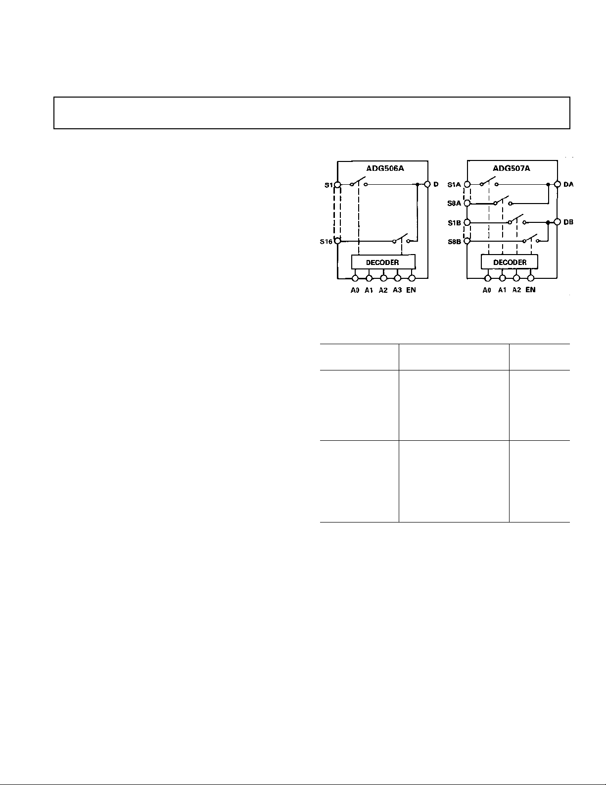
The ADG506A and ADG507A are CMOS monolithic analog
multiplexers with 16 channels and dual 8 channels, respectively.
The ADG506A switches one of 16 inputs to a common output,
depending on the state of four binary addresses and an enable
input. The ADG507A switches one of eight differential inputs to
a common differential output, depending on the state of three
binary addresses and an enable input. Both devices have TTL
and 5 V CMOS logic compatible digital inputs.
The ADG506A and ADG507A are designed on an enhanced
2
LC
MOS process, which gives an increased signal capability of
to VDD and enables operation over a wide range of supply
V
SS
voltages. The devices can operate comfortably anywhere in the
10.8 V to 16.5 V single or dual supply range. These multiplexers
also feature high switching speeds and low R
PRODUCT HIGHLIGHTS
1. Single/Dual Supply Specifications with a Wide Tolerance
The devices are specified in the 10.8 V to 16.5 V range for
both single and dual supplies.
2. Extended Signal Range
The enhanced LC
down and an increased analog signal range of V
3. Break-Before-Make Switching
Switches are guaranteed break-before-make so input signals
are protected against momentary shorting.
4. Low Leakage
Leakage currents in the range of 20 pA make these multiplexers
suitable for high precision circuits.
2
MOS processing results in a high break-
ON
.
to VDD.
SS
8-/16-Channel Analog Multiplexers
ADG506A/ADG507A
FUNCTIONAL BLOCK DIAGRAM
ORDERING GUIDE
1
Model
ADG506AKN –40°C to +85°C N-28
ADG506AKR –40°C to +85°C R-28
ADG506AKP –40°C to +85°C P-28A
ADG506ABQ –40°C to +85°C Q-28
ADG506ATQ –55°C to +125°C Q-28
ADG506ATE –55°C to +125°C E-28A
ADG507AKN –40°C to +85°C N-28
ADG507AKR –40°C to +85°C R-28
ADG507AKP –40°C to +85°C P-28A
ADG507AKRU –40°C to +85°C RU-28
ADG507ABQ –40°C to +85°C Q-28
ADG507ATQ –55°C to +125°C Q-28
ADG507ATE –55°C to +125°C E-28A
NOTES
1
To order MIL-STD-883, Class B processed parts, add /883B to part number.
See Analog Devices’ Military/Aerospace Reference Manual (1994) for military
data sheet.
2
E = Leadless Ceramic Chip Carrier (LCCC); N = Plastic DIP; P = Plastic
Leaded Chip Carrier (PLCC); Q = Cerdip; R = 0.3" Small Outline IC (SOIC);
RU = Thin Shrink Small Outline Package (TSSOP).
Temperature Package
Range Option
2
REV. C
Information furnished by Analog Devices is believed to be accurate and
reliable. However, no responsibility is assumed by Analog Devices for its
use, nor for any infringements of patents or other rights of third parties
which may result from its use. No license is granted by implication or
otherwise under any patent or patent rights of Analog Devices.
One Technology Way, P.O. Box 9106, Norwood, MA 02062-9106, U.S.A.
Tel: 781/329-4700 World Wide Web Site: http://www.analog.com
Fax: 781/326-8703 © Analog Devices, Inc., 1998

ADG506A/ADG507A–SPECIFICATIONS
Dual Supply
(VDD = +10.8 V to +16.5 V, VSS = –10.8 V to –16.5 V unless otherwise noted)
ADG506A ADG506A ADG506A
ADG507A ADG507A ADG507A
K Version B Version T Version
–40ⴗC to –40ⴗC to –55ⴗC to
Parameter +25ⴗC +85ⴗC +25ⴗC +85ⴗC +25ⴗC +125ⴗC Units Comments
ANALOG SWITCH
Analog Signal Range V
R
ON
V
SS
DD
SS
V
DD
V
280 280 280 Ω typ –10 V ≤ VS ≤ +10 V, I
V
V
SS
DD
V
SS
V
DD
V
SS
V
DDVDD
V
SS
V min
V max
450 600 450 600 450 600 Ω max
= 1 mA; Test Circuit 1
DS
300 400 300 400 Ω max VDD = 15 V (±10%), VSS = –15 V (±10%)
300 400 Ω max VDD = 15 V (±5%), VSS = –15 V (±5%)
R
Drift 0.6 0.6 0.6 %/°C typ –10 V ≤ VS ≤ +10 V, I
ON
R
Match 5 5 5 % typ –10 V ≤ VS ≤ +10 V, I
ON
I
(OFF), Off Input Leakage 0.02 0.02 0.02 nA typ V1 = ±10 V, V2 = ⫿10 V; Test Circuit 2
S
I
(OFF), Off Output Leakage 0.04 0.04 0.04 nA typ V1 = ±10 V, V2 = ⫿10 V; Test Circuit 3
D
ADG506A 1 200 1 200 1 200 nA max
1 50 1 50 1 50 nA max
= 1 mA
DS
= 1 mA
DS
ADG507A 1 100 1 100 1 100 nA max
I
(ON), On Channel Leakage 0.04 0.04 0.04 nA typ V1 = ±10 V, V2 = ⫿10 V; Test Circuit 4
D
ADG506A 1 200 1 200 1 200 nA max
ADG507A 1 100 1 100 1 100 nA max
I
, Differential Off Output
DIFF
Leakage (ADG507A Only) 25 25 25 nA max V1 = ±10 V, V2 = ⫿10 V; Test Circuit 5
DIGITAL CONTROL
V
, Input High Voltage 2.4 2.4 2.4 V min
INH
V
, Input Low Voltage 0.8 0.8 0.8 V max
INL
I
or I
INL
INH
CIN Digital Input Capacitance 8 8 8 pF max
DYNAMIC CHARACTERISTICS
t
TRANSITION
t
OPEN
tON (EN)
t
OFF
1
(EN)
1
1
1
OFF Isolation 68 68 68 dB typ VEN = 0.8 V, R
111µA max V
= 0 to V
IN
DD
200 200 200 ns typ V1 = ±10 V, V2 = +10 V; Test Circuit 6
300 400 300 400 300 400 ns max
50 50 50 ns typ Test Circuit 7
25 10 25 10 25 10 ns min
200 200 200 ns typ Test Circuit 8
300 400 300 400 300 400 ns max
200 200 200 ns typ Test Circuit 8
300 400 300 400 300 400 ns max
= 1 kΩ, C
50 50 50 dB min VS = 7 V rms, f = 100 kHz
L
= 15 pF,
L
CS (OFF) 5 5 5 pF typ VEN = 0.8 V
CD (OFF)
ADG506A 44 44 44 pF typ VEN = 0.8 V
ADG507A 22 22 22 pF typ
Q
, Charge Injection 4 4 4 pC typ R
INJ
= 0 Ω, V
S
= 0 V; Test Circuit 9
S
POWER SUPPLY
I
DD
I
SS
0.6 0.6 0.6 mA typ VIN = V
1.5 1.5 1.5 mA max
20 20 20 µA typ V
0.2 0.2 0.2 mA max
= VIN or V
IN
INL
or V
lNH
INH
Power Dissipation 10 10 10 mW typ
28 28 28 mW max
NOTES
1
Sample tested at +25°C to ensure compliance.
Specifications subject to change without notice.
–2–
REV. C

ADG506A/ADG507A
Single Supply
Parameter +25ⴗC +85ⴗC +25ⴗC +85ⴗC +25ⴗC +125ⴗC Units Comments
ANALOG SWITCH
Analog Signal Range V
R
ON
R
Drift 0.6 0.6 0.6 %/°C typ 0 V ≤ VS ≤ +10 V, I
ON
R
Match 5 5 5 % typ 0 V ≤ VS ≤ +10 V, I
ON
IS (OFF), Off Input Leakage 0.02 0.02 0.02 nA typ V1 = +10 V/0 V, V2 = 0 V/ +10 V;
ID (OFF), Off Output Leakage 0.04 0.04 0.04 nA typ V1 = +10 V/0 V, V2 = 0 V/ +10 V;
ADG506A 1 200 1 200 1 200 nA max Test Circuit 3
ADG507A 1 100 1 100 1 100 nA max
ID (ON), On Channel Leakage 0.04 0.04 0.04 nA typ V1 = +10 V/0 V, V2 = 0 V/ +10 V;
ADG506A 1 200 1 200 1 200 nA max Test Circuit 4
ADG507A 1 100 1 100 1 100 nA max
I
, Differential Off Output V1 = +10 V/0 V, V2 = 0 V/ +10 V;
DIFF
Leakage (ADG507A Only) 25 25 25 nA max Test Circuit 5
DIGITAL CONTROL
V
, Input High Voltage 2.4 2.4 2.4 V min
INH
V
, Input Low Voltage 0.8 0.8 0.8 V max
INL
I
or I
INL
INH
CIN Digital Input Capacitance 8 8 8 pF max
DYNAMIC CHARACTERISTICS
t
TRANSITION
t
OPEN
tON (EN)
t
OFF
OFF Isolation 68 68 68 dB typ VEN = 0.8 V, R
CS (OFF) 5 5 5 pF typ VEN = 0.8 V
CD (OFF)
Q
INJ
POWER SUPPLY
I
DD
Power Dissipation 10 10 10 mW typ
NOTES
1
Sample tested at +25°C to ensure compliance.
Specifications subject to change without notice.
1
1
1
1
(EN)
ADG506A 44 44 44 pF typ VEN = 0.8 V
ADG507A 22 22 22 pF typ
, Charge Injection 4 4 4 pC typ R
(VDD = +10.8 V to +16.5 V, VSS = GND = 0 V unless otherwise noted)
ADG506A ADG506A ADG506A
ADG507A ADG507A ADG507A
K Version B Version T Version
–40ⴗC to –40ⴗC to –55ⴗC to
V
SS
DD
SS
V
DD
V
500 500 500 Ω typ 0 V ≤ VS ≤ +10 V, I
V
V
SS
DD
V
SS
V
DD
V
SS
V
DDVDD
V
SS
700 1000 700 1000 700 1000 Ω max
1 50 1 50 1 50 nA max Test Circuit 2
111µA max V
300 300 300 ns typ V1 = +10 V/0 V, V2 = +10 V; Test Circuit 6
450 600 450 600 450 600 ns max
50 50 50 ns typ Test Circuit 7
25 10 25 10 25 10 ns min
250 250 250 ns typ Test Circuit 8
450 600 450 600 450 600 ns max
250 250 250 ns typ Test Circuit 8
450 600 450 600 450 600 ns max
50 50 50 dB min VS = 3.5 V rms, f = 100 kHz
0.6 0.6 0.6 mA typ VIN = V
1.5 1.5 1.5 mA max
25 25 25 mW max
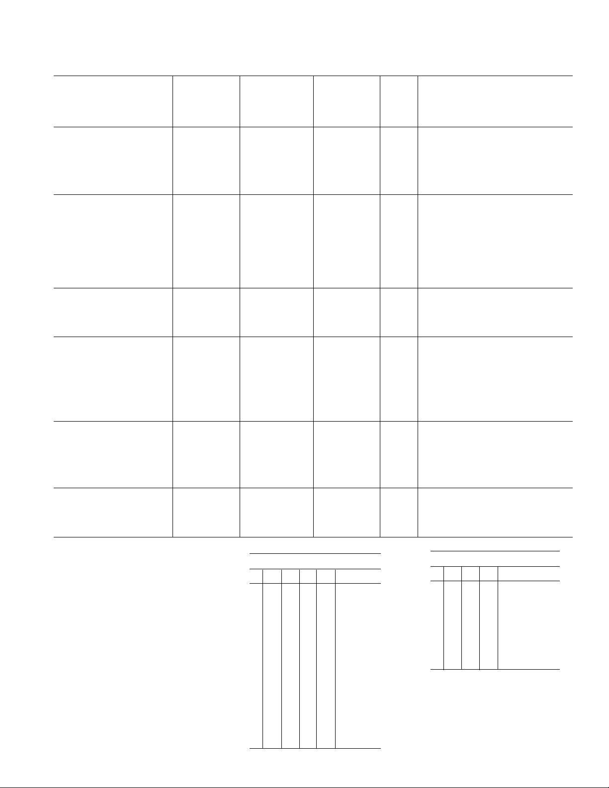
Truth Table (ADG506A)
A3 A2 A1 A0 EN On Switch
XXXX0 NONE
000011
000112
001013
001114
010015
010116
011017
011118
100019
1001110
1010111
1011112
1100113
1101114
1110115
1111116
V min
V max
X = Don’t Care
= 0.5 mA; Test Circuit 1
DS
= 0.5 mA
DS
= 0.5 mA
DS
= 0 to V
IN
= 0 Ω, V
S
DD
= 1 kΩ, C
L
= 0 V; Test Circuit 9
S
or V
INL
lNH
= 15 pF,
L
Truth Table (ADG507A)
A2 A1 A0 EN On Switch Pair
XXX0 NONE
00011
00112
01013
01114
10015
10116
11017
11118
REV. C
–3–
 Loading...