Analog Devices ADG465 Datasheet

Single Channel Protector
a
FEATURES
Fault and Overvoltage Protection up to ⴞ40␣ V
Signal Paths Open Circuit with Power Off
Signal Path Resistance of R
44 V Supply Maximum Ratings
Low On Resistance 80 ⍀ Typ
1 nA Max Path Current Leakage @ +25ⴗC
Low Power Dissipation 0.8␣ W Typ
Latchup-Proof Construction
APPLICATIONS
ATE Equipment
Sensitive Measurement Equipment
Hot-Insertion Rack Systems
ADC Input Channel Protection
GENERAL DESCRIPTION
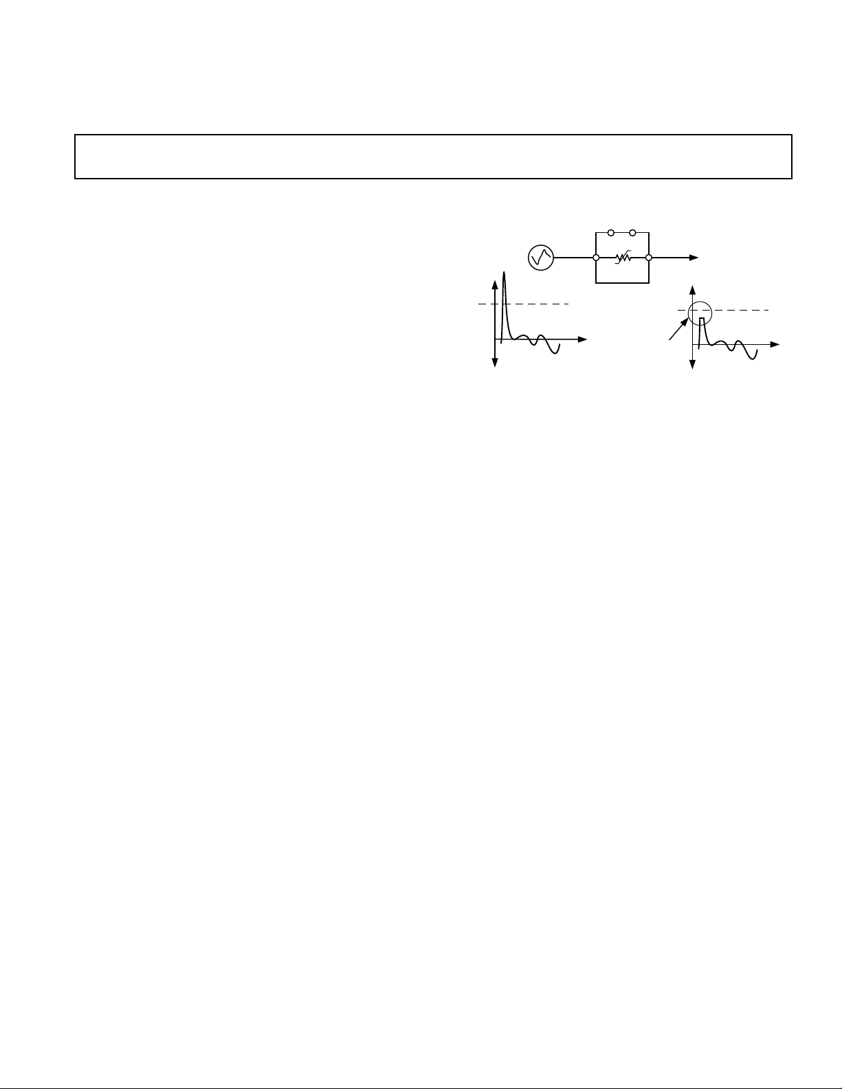
The ADG465 is a single channel protector in an SOT-23 package. The channel protector is placed in series with the signal
path, and will protect sensitive components from voltage transience in the signal path whether or not the power supplies are
present. Because the channel protection works regardless of the
presence of the supplies, the channel protectors are ideal for use
in applications where correct power sequencing cannot always
be guaranteed to protect analog inputs (e.g., hot-insertion rack
systems). This is discussed further, and some example circuits
are given, in the Applications section of this data sheet.
A channel protector consists of an n-channel MOSFET, a
p-channel MOSFET and an n-channel MOSFET, connected in
series. The channel protector behaves like a series resistor during normal operation, i.e., (V
+ 2 V) < VIN < (VDD – 1.5 V).
SS
When a channel’s analog input exceeds the power supplies
(including V
and VSS = 0 V), one of the MOSFETs will
DD
switch off, clamping the output to either V
Circuitry and signal source protection is provided in the event of
an overvoltage or power loss. The channel protectors can withstand overvoltage inputs from –40 V to +40 V. See the Circuit
Information section of this data sheet.
The ADG465 can operate from both bipolar and unipolar
supplies. The channels are normally on when power is connected, and open circuit when power is disconnected. With
power supplies of ±15 V, the on-resistance of the ADG465 is
80 Ω typ, with a leakage current of ±1 nA max. When power
is disconnected, the input leakage current is approximately
±5 nA typ.
The ADG465 is available in a 6-lead plastic surface mount
SOT-23 package, and an 8-lead µSOIC package.
with Power On
ON
+ 2 V or VDD – 1.5 V.
SS
in an SOT-23 Package
ADG465
FUNCTIONAL BLOCK DIAGRAM
VDDV
SS
V
V
IN
V
IN
V
DD
D1
ADG465
OUTPUT CLAMPED
@ V
PRODUCT HIGHLIGHTS
1. Fault Protection.
The ADG465 can withstand continuous voltage inputs from
–40 V to +40 V. When a fault occurs due to the power supplies being turned off, or due to an overvoltage being applied
to the ADG465, the output is clamped. When power is turned
off, current is limited to the nanoampere level.
2. Low Power Dissipation.
3. Low R
80 Ω typ.
ON
4. Trench Isolation Latchup-Proof Construction.
A dielectric trench separates the p- and n-channel MOSFETs
thereby preventing latchup.
DD
– 1.5V
V
S1
V
OUT
V
OUT
V
DD
REV. A
Information furnished by Analog Devices is believed to be accurate and
reliable. However, no responsibility is assumed by Analog Devices for its
use, nor for any infringements of patents or other rights of third parties
which may result from its use. No license is granted by implication or
otherwise under any patent or patent rights of Analog Devices.
One Technology Way, P.O. Box 9106, Norwood, MA 02062-9106, U.S.A.
Tel: 781/329-4700 World Wide Web Site: http://www.analog.com
Fax: 781/326-8703 © Analog Devices, Inc., 1998

ADG465–SPECIFICATIONS
Dual Supply
Parameter +25ⴗC B Units Test Conditions/Comments
FAULT PROTECTED CHANNEL
Fault-Free Analog Signal Range
R
ON
∆R
ON
LEAKAGE CURRENTS
Channel Output Leakage, I
(Without Fault Condition) ±0.1 ±1 nA typ
Channel Input Leakage, I
(With Fault Condition) ±0.2 ±0.4 nA typ V
Channel Input Leakage, I
(With Power Off and Fault) ±0.5 ±2 nA typ V
Channel Input Leakage, I
(With Power Off and Output S/C) ±0.005 ±0.1 µA typ V
POWER REQUIREMENTS
I
DD
I
SS
V
DD/VSS
NOTES
1
Temperature range is as follows: B Version: – 40°C to +85°C.
2
Guaranteed by design, not subject to production test.
Specifications subject to change without notice.
1
(VDD = +15 V, VSS = –15 V, GND = 0 V, unless otherwise noted)
2
VSS + 1.2 V min Output Open Circuit
– 0.8 V max
V
DD
80 Ω typ –10 V ≤ VS ≤ +10 V, I
95 115 Ω max
45 Ω max –5 V ≤ VS ≤ +5 V
S(ON)
±1 ±5 nA max
D(ON)
±2 ±5 nA max
D(OFF)
±2 ±10 nA max V
D(OFF)
±0.015 ±0.5 µA max
±0.05 µA typ
±0.5 ±5 µA max
±0.05 µA typ
±0.5 ±5 µA max
0 0 V min
±20 ±20 V max
VS = V
V
= ±10 V
D
= ±25 V
S
= Open Circuit
D
VDD = 0 V, V
= ±35 V
S
= Open Circuit
D
VDD = 0 V, V
= ±35 V, V
S
= 0 V
SS
= 0 V
SS
= 0 V
D
= 1 mA
S
–2–
–2–
REV. A
REV. A

ADG465
ABSOLUTE MAXIMUM RATINGS
(T
= +25°C unless otherwise noted)
A
VDD to VSS . . . . . . . . . . . . . . . . . . . . . . . . . . . . . . . . . . . +44 V
V
, VD, Analog Input Overvoltage with Power ON
S
. . . . . . . . . . . . . . . . . . . . . . . . . VSS – 20 V to VDD + 20 V
, VD, Analog Input Overvoltage with Power OFF
V
S
1
2
2
. . . . . . . . . . . . . . . . . . . . . . . . . . . . . . . . . . . –35 V to +35 V
Continuous Current, S or D . . . . . . . . . . . . . . . . . . . . .20 mA
Peak Current, S or D . . . . . . . . . . . . . . . . . . . . . . . . . . .40 mA
(Pulsed at 1 ms, 10% Duty Cycle Max)
Operating Temperature Range
Industrial (B Version) . . . . . . . . . . . . . . . . –40°C to +85°C
Storage Temperature Range . . . . . . . . . . . . –65°C to +125°C
Junction Temperature . . . . . . . . . . . . . . . . . . . . . . . . .+150°C
SOT-23 Package
, Thermal Impedance . . . . . . . . . . . . . . . . . . . 230°C/W
θ
JA
µSOIC Package
, Thermal Impedance . . . . . . . . . . . . . . . . . . . 205°C/W
θ
JA
Lead Temperature, Soldering
Vapor Phase (60 sec) . . . . . . . . . . . . . . . . . . . . . .+215°C
Infrared (15 sec) . . . . . . . . . . . . . . . . . . . . . . . . . .+220°C
NOTES
1
Stresses above those listed under Absolute Maximum Ratings may cause perma-
nent damage to the device. This is a stress rating only; functional operation of the
device at these or any other conditions above those listed in the operational
sections of this specification is not implied. Exposure to absolute maximum rating
conditions for extended periods may affect device reliability. Only one absolute
maximum rating may be applied at any one time.
2
Overvoltages at S or D will be clamped by the channel protector, see Circuit
Information section of the data sheet.
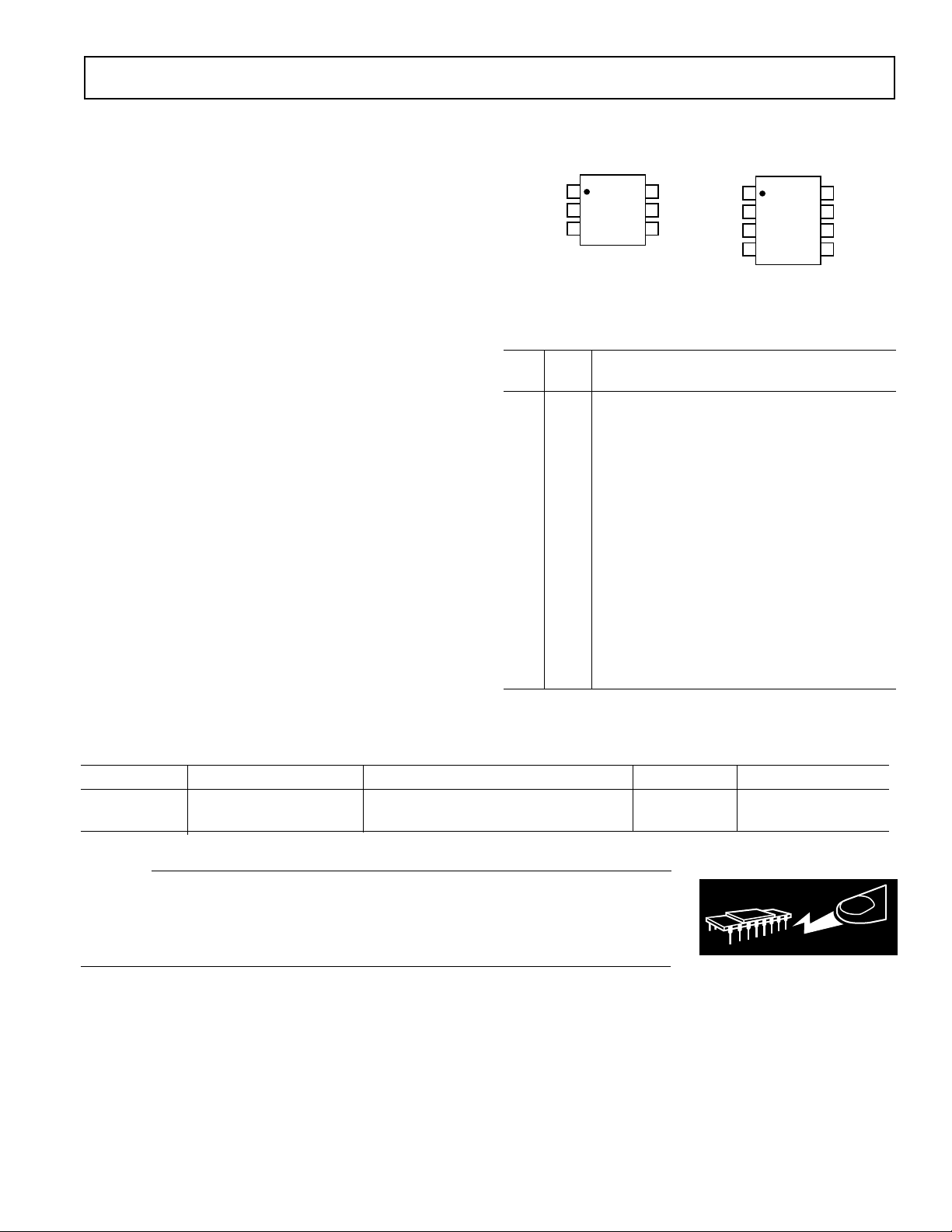
PIN CONFIGURATIONS
(RT-6)
V
1
D1
ADG465
NC
2
TOP VIEW
(Not to Scale)
V
3
SS
NC = NO CONNECT
6
V
DD
5
NC
4
V
S1
(RM-8)
1
NC
ADG465
V
2
DD
TOP VIEW
(Not to Scale)
V
3
S1
45
NC = NO CONNECT
PIN FUNCTION DESCRIPTIONS
Pin Pin
RT-6 RM-8 Pin Description
17 V
, this is one terminal of the channel protec-
D1
tor. The channel protector is bidirectional so this
terminal may be used as an input or an output.
2 1, 4 NC, this is a no connect pin.
36 V
, Negative Power Supply (0 V to –20 V).
SS
The clamping point for a negative overvoltage is
also defined by V
, see Overvoltage Protection
SS
section.
43 V
, this is one terminal of the channel protec-
S1
tor. The channel protector is bidirectional so this
terminal may be used as an output or an input.
5 5, 8 NC, this is a no connect pin.
62 V
, Positive Power Supply (0 V to 20 V). The
DD
clamping point for a positive overvoltage is also
defined by V
, see Overvoltage Protection
DD
section.
8
NC
V
7
D1
V
6
SS
NCNC
ORDERING GUIDE
Model Temperature Range Package Descriptions Brand Package Options
ADG465BRT –40°C to +85°C 6-Lead Plastic Surface Mount SOT-23 S1B RT-6
ADG465BRM –40°C to +85°C 8-Lead µSOIC S1B RM-8
CAUTION
ESD (electrostatic discharge) sensitive device. Electrostatic charges as high as 4000 V readily
accumulate on the human body and test equipment and can discharge without detection.
WARNING!
Although the ADG465 features proprietary ESD protection circuitry, permanent damage may
occur on devices subjected to high energy electrostatic discharges. Therefore, proper ESD
precautions are recommended to avoid performance degradation or loss of functionality.
REV. A
–3–
ESD SENSITIVE DEVICE
 Loading...