

Power-Off Protection ±5 V, +12 V, Quad
SPST Switches with 5 Ω On Resistance
FEATURES
Power-off protection
Switch guaranteed off with no power supplies present
Inputs are high impedance with no power
Switch turns off when input > V
Overvoltage protection up to 16 V
PSS robust
Negative signal capability passes signals down to −5.5 V
6.1 Ω maximum on resistance
1.4 Ω on-resistance flatness
±3 V to ±5.5 V dual supply
3 V to 12 V single supply
3 V logic compatible inputs
Rail-to-rail operation
16-lead TSSOP and 16-lead 3 mm × 3 mm LFCSP
APPLICATIONS
Hot swap applications
Data acquisition systems
Battery-powered systems
Automatic test equipment
Communication systems
Relay replacement
GENERAL DESCRIPTION
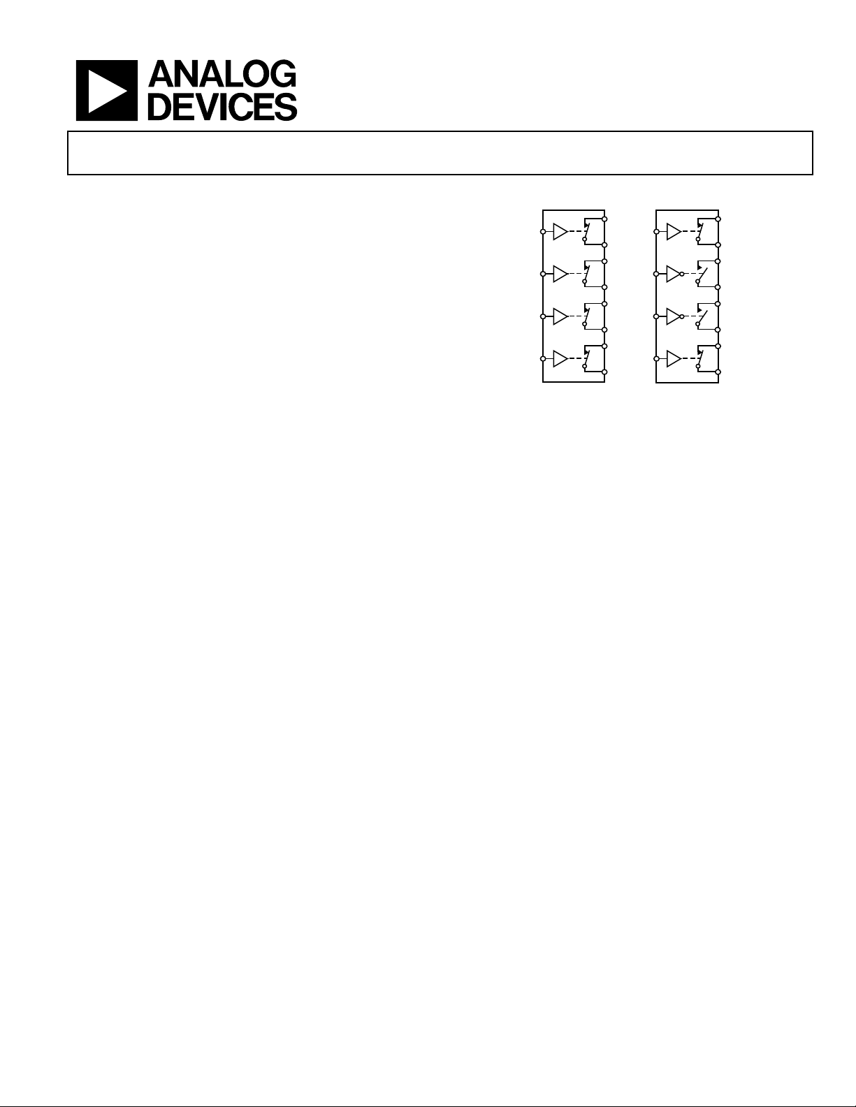
The ADG4612/ADG4613 contain four independent singlepole/single-throw (SPST) switches. The ADG4612 switches are
turned on with Logic 1 on the appropriate control input. The
ADG4613 has two switches with digital control logic similar to
that of the ADG4612; the logic is inverted on the other two
switches. Each switch conducts equally well in both directions
when on, and each switch has an input signal range that extends
to the supplies. The ADG4613 exhibits break-before-make
switching action for use in multiplexer applications.
When no power supplies are present, the switch remains in the
off condition, and the switch inputs are high impedance inputs,
ensuring that no current flows, which can damage the switch or
downstream circuitry. This is very useful in applications where
analog signals may be present at the switch inputs before power
is applied or where the user has no control over the power supply
sequence.
In the off condition, signal levels up to 16 V are blocked. Also,
when the analog input signal levels exceed V
turns off.
DD
+ VT
by VT, the switch
DD
ADG4612/ADG4613
FUNCTIONAL BLOCK DIAGRAM
S1
IN1
IN2
ADG4612
IN3
IN4
SWITCHES SHOWN FOR A LOGIC 1 INPUT.
D1
S2
D2
S3
D3
S4
D4
Figure 1.
IN1
IN2
ADG4613
IN3
IN4
The low on resistance of these switches make them ideal
solutions for data acquisition and gain switching applications
where low on resistance and distortion is critical. The onresistance profile is very flat over the full analog input range
ensuring excellent linearity and low distortion when switching
audio signals.
PRODUCT HIGHLIGHTS
1. Power-Off Protection On Both S and D Pins.
2. PSS Robustness.
3. Overvoltage Protection up to 16 V.
4. 5.2 Ω On Resistance.
5. 16-Lead TSSOP and 3 mm × 3 mm LFCSP Packages.
S1
D1
S2
D2
S3
D3
S4
D4
09005-001
Rev. 0
Information furnished by Analog Devices is believed to be accurate and reliable. However, no
responsibility is assumed by Anal og Devices for its use, nor for any infringements of patents or ot her
rights of third parties that may result from its use. Specifications subject to change without notice. No
license is granted by implication or otherwise under any patent or patent rights of Analog Devices.
Trademarks and registered trademarks are the property of their respective owners.
One Technology Way, P.O. Box 9106, Norwood, MA 02062-9106, U.S.A.
Tel: 781.329.4700 www.analog.com
Fax: 781.461.3113 ©2010 Analog Devices, Inc. All rights reserved.

ADG4612/ADG4613
TABLE OF CONTENTS
Features.............................................................................................. 1
Applications....................................................................................... 1
General Description ......................................................................... 1
Functional Block Diagram .............................................................. 1
Product Highlights ........................................................................... 1
Specifications..................................................................................... 3
5 V Dual Supply............................................................................ 3
12 V Single Supply........................................................................ 5
5 V Single Supply.......................................................................... 7
Continuous Current Per Channel, Sx or Dx............................. 8
Power Supply Operation.............................................................. 8
Absolute Maximum Ratings............................................................ 9
REVISION HISTORY
10/10—Revision 0: Initial Version
Thermal Resistance.......................................................................9
ESD Caution...................................................................................9
Pin Configurations and Function Descriptions......................... 10
Typical Performance Characteristics........................................... 11
Test Circuits..................................................................................... 14
Terminology.................................................................................... 16
Theory of Operation ...................................................................... 17
Bipolar Operation and Single-Supply Operation................... 18
Applications Information.............................................................. 19
Outline Dimensions....................................................................... 21
Ordering Guide .......................................................................... 22
Rev. 0 | Page 2 of 24

ADG4612/ADG4613
SPECIFICATIONS
5 V DUAL SUPPLY
VDD = +5 V ± 10%, VSS = −5 V ± 10%, GND = 0 V, unless otherwise noted.
Table 1.
Parame ter 25°C −40°C to +85°C Unit Test Conditions/Comments
ANALOG SWITCH
Analog Signal Range (Normal Mode) −5.5 V to VDD V V
On Resistance (RON) 5.2 Ω typ VS = ±4.5 V, IS = −10 mA; see Figure 22
6.1 7.6 Ω max VDD = +4.5 V, VSS = −4.5 V
On-Resistance Match Between Channels
(∆R
)
ON
0.05 Ω typ V
0.15 0.18 Ω max
On-Resistance Flatness (R
) 1.4 Ω typ VS = ±4.5 V, IS = −10 mA
FLAT (ON)
1.75 2.2 Ω max
LEAKAGE CURRENTS (NORMAL MODE) VDD = +5.5 V, VSS = −5.5 V
Source Off Leakage, IS (Off) ±5 nA typ
±10 ±300 nA max
Drain Off Leakage, ID (Off) ±5 nA typ
±10 ±300 nA max
Channel On Leakage, ID (On), IS (On) ±10 nA typ VS = VD = ±4.5 V; see Figure 24
±16 ±700 nA max
LEAKAGE CURRENTS (ISOLATION MODE)
Source Off Leakage, IS (Off) ±0.03 μA typ VDD = 0 V or floating, VSS = 0 V or floating, GND = 0 V
±0.1 ±2.5 μA max
±8 μA typ VDD = +5.5 V, VSS = −5.5 V or 0 V
±22 ±30 μAmax
Drain Off Leakage, ID (Off) ±0.03 μA typ VDD = 0 V or floating, VSS = 0 V or floating, GND = 0 V
±0.1 ±2.5 μA max
±8 μA typ VDD = +5.5 V, VSS = −5.5 V or 0 V
±22 ±30 μA max
DIGITAL INPUTS
Input High Voltage, V
Input Low Voltage, V
Input Current, I
INL
2.0 V min
INH
0.8 V max
INL
±0.015 μA typ VIN = V
±0.1 ±0.15 μA max
Input Current, I
±13 μA typ VIN = VDD
INH
±16 ±18 μA max
Logic Pull-Down Resistance, RPD 400 kΩ typ
Digital Input Capacitance, CIN 4 pF typ
DYNAMIC CHARACTERISTICS1
tON 73 ns typ RL = 300 Ω, CL = 35 pF
125 149 ns max VS = 3 V; see Figure 25
t
100 ns typ RL = 300 Ω, CL = 35 pF
OFF
125 149 ns max VS = 3 V; see Figure 25
to V
= 16 V maximum
DD
SS
= ±4.5 V, IS = −10 mA
S
V
= ±4.5 V, VD = ט4.5 V; see Figure 23
S
V
= ±4.5 V, VD = ט4.5 V; see Figure 23
S
= −5.5 V, VD = +10.5 V; or VS = +10.5 V, VD = −5.5 V;
V
S
see Figure 23
= −5.5 V, VD = +10.5 V; or VS = +10.5 V, VD = −5.5 V;
V
S
see Figure 23
= −5.5 V, VD = +10.5 V; or VS = +10.5 V, VD = −5.5 V;
V
S
see Figure 23
= −5.5 V, VD = +10.5 V; or VS = +10.5 V, VD = −5.5 V;
V
S
see Figure 23
GND
Rev. 0 | Page 3 of 24

ADG4612/ADG4613
Parame ter 25°C −40°C to +85°C Unit Test Conditions/Comments
Break-Before-Make Time Delay, tD 20 ns typ RL = 50 Ω, CL = 35 pF
(ADG4613 Only) 3 ns min VS1 = VS2 = 3 V; see Figure 26
Fault Response Time 295 ns typ VS = 2 V to 8 V, RL = 300 Ω, CL = 35 pF
Fault Recovery Time 1.2 μs typ VS = 2 V to 8 V, RL = 300 Ω, CL = 35 pF
Threshold Voltage, VT 1.8 V typ
Charge Injection 225 pC typ VS = 0 V, RS = 0 Ω, CL = 1 nF; see Figure 27
Off Isolation −54 dB typ RL = 50 Ω, CL = 5 pF, f = 1 MHz; see Figure 28
Channel-to-Channel Crosstalk −71 dB typ RL = 50 Ω, CL = 5 pF, f = 1 MHz; see Figure 29
Total Harmonic Distortion + Noise, THD + N 0.13 % typ
Insertion Loss −0.5 dB typ RL = 50 Ω, CL = 5 pF; f = 1 MHz; see Figure 30
−3 dB Bandwidth 293 MHz typ RL = 50 Ω, CL = 5 pF; see Figure 30
CS (Off) 13 pF typ VS = 0 V, f = 1 MHz
CD (Off) 13 pF typ VS = 0 V, f = 1 MHz
CD (On), CS (On) 50 pF typ VS = 0 V, f = 1 MHz
POWER REQUIREMENTS
Normal Mode Digital inputs = 0 V or VDD
IDD 90 μA typ VDD = +5.5 V, VSS = −5.5 V
140 165 μA max
ISS 27 μA typ VDD = +5.5 V, VSS = −5.5 V
50 58 μA max
Isolation Mode VDD = +5.5 V, VSS = −5.5 V or floating
IDD 90 μA typ Digital inputs = 0 V or 5.5 V
140 165 μA max VS = −5.5 V or +10.5 V
V
ISS 0.1 μA typ Digital inputs = 0 V or 5.5 V
0.2 6 μA max VS = −5.5 V or +10.5 V
1
Guaranteed by design; not subject to production test.
= 110 Ω, 6 V p-p, f = 20 Hz to 20 kHz;
R
L
see Figure 31
= 0 V or floating, VSS = −5.5 V
DD
Rev. 0 | Page 4 of 24

ADG4612/ADG4613
12 V SINGLE SUPPLY
VDD = 12 V ± 10%, VSS = 0 V, GND = 0 V, unless otherwise noted.
Table 2.
Parameter 25°C −40°C to +85°C Unit Test Conditions/Comments
ANALOG SWITCH
Analog Signal Range −5.5 V to VDD V V
On-Resistance (RON) 4.5 Ω typ VS = 0 V to +10 V, IS = −10 mA; see Figure 22
5.1 6.4 Ω max VDD = 10.8 V, VSS = 0 V
On-Resistance Match Between Channels
(∆R
)
ON
0.05 Ω typ VS = 0 V to +10 V, IS = −10 mA
0.15 0.18 Ω max
On-Resistance Flatness (R
) 1 Ω typ VS = 0 V to +10 V, IS = −10 mA
FLAT (ON)
1.25 1.6 Ω max
LEAKAGE CURRENTS
Normal Mode VDD = 13.2 V, VSS = 0 V
Source Off Leakage, IS (Off) ±3 nA typ VS = 1 V/10 V, VD = 10 V/1 V; see Figure 23
±10 ±200 nA max
Drain Off Leakage, ID (Off) ±3 nA typ VS = 1 V/10 V, VD = 10 V/1 V; see Figure 23
±10 ±200 nA max
Channel On Leakage, ID (On), IS (On) ±7 nA typ VS = VD = 1 V or 10 V; Figure 24
±11 ±300 nA max
Isolation Mode
Source Off Leakage, IS (Off) ±0.05 μA typ
±0.3 ±3 μA max VS = 1 V/16 V, VD = 16 V/1 V; see Figure 23
±10
μA typ
±28 ±38 μA max
Drain Off Leakage, ID (Off) ±0.05 μA typ
±0.3 ±3 μA max
±10 μA typ
±28 ±38 μA max
DIGITAL INPUTS
Input High Voltage, V
Input Low Voltage, V
Input Current, I
INL
2.0 V min
INH
0.8 V max
INL
±0.015 μA typ VIN = V
±0.1 ±0.15 μA max
Input Current, I
±13 μA typ VIN = 5 V
INH
±16 ±18 μA max
Input Current, I
±34 μA typ VIN = VDD
INH
±40 ±42 μA max
Logic Pull-Down Resistance, RPD 400 kΩ typ
Digital Input Capacitance, CIN 4 pF typ
DYNAMIC CHARACTERISTICS1
tON 46 ns typ RL = 300 Ω, CL = 35 pF
73 90 ns max VS = 8 V; see Figure 25
t
70 ns typ RL = 300 Ω, CL = 35 pF
OFF
91 103 ns max VS = 8 V; see Figure 25
to V
= 16 V maximum
DD
SS
= 0 V or floating, VSS = 0 V or floating,
V
DD
GND = 0 V
= 13.2 V, VSS = 0 V, VS = 16 V/1 V, VD = 1 V/16 V;
V
DD
see Figure 23
= 0 V or floating, VSS = 0 V or floating,
V
DD
GND = 0 V V
= 1 V/16 V, VD = 16 V/1 V;
S
see Figure 23
= 13.2 V, VSS = 0 V
V
DD
= 16 V/1 V, VD = 1 V/16 V; see Figure 23
V
S
GND
Rev. 0 | Page 5 of 24

ADG4612/ADG4613
Parameter 25°C −40°C to +85°C Unit Test Conditions/Comments
Break-Before-Make Time Delay, tD 17 ns typ RL = 50 Ω, CL = 35 pF
(ADG4613 Only) 11 ns min VS1 = VS2 = 8 V; see Figure 26
Fault Response Time 250 ns typ VS = 9 V to 15 V, RL = 300 Ω, CL = 35 pF
Fault Recovery Time 1.4 μs typ VS = 9 V to 15 V, RL = 300 Ω, CL = 35 pF
Threshold Voltage, VT 1.8 V typ
Charge Injection 292 pC typ VS = 6 V, RS = 0 Ω, CL = 1 nF; see Figure 27
Off Isolation −56 dB typ RL = 50 Ω, CL = 5 pF, f = 1 MHz; see Figure 28
Channel-to-Channel Crosstalk −74 dB typ RL = 50 Ω, CL = 5 pF, f = 1 MHz; see Figure 29
Total Harmonic Distortion + Noise, THD + N 0.26 % typ
Insertion Loss −0.27 dB typ RL = 50 Ω, CL = 5 pF; f = 1 MHz; see Figure 30
−3 dB Bandwidth 250 MHz typ RL = 50 Ω, CL = 5 pF; see Figure 30
CS (Off) 11.5 pF typ VS = 0 V, f = 1 MHz
CD (Off) 11.5 pF typ VS = 0 V, f = 1 MHz
CD (On), CS (On) 48 pF typ VS = 0 V, f = 1 MHz
POWER REQUIREMENTS
Normal Mode VDD = 13.2 V, VSS = 0 V
IDD 90 μA typ Digital inputs = 0 V or VDD
140 165 μA max
IDD 600 μA typ Digital inputs = 5 V
660 900 μA max
Isolation Mode VDD = 13.2 V, VSS = 0 V or floating
IDD 90 μA typ VS = 16 V or 1 V
140 165 μA max Digital inputs = 0 V or VDD
1
Guaranteed by design, not subject to production test.
= 110 Ω, 6 V p-p, f = 20 Hz to 20 kHz; see
R
L
Figure 31
Rev. 0 | Page 6 of 24

ADG4612/ADG4613
5 V SINGLE SUPPLY
VDD = 5 V ± 10%, VSS = 0 V, GND = 0 V, unless otherwise noted.
Table 3.
Parameter 25°C −40°C to +85°C Unit Test Conditions/Comments
ANALOG SWITCH
Analog Signal Range −5.5 V to VDD V V
On-Resistance (RON) 12.5 Ω typ VS = 0 V to +4.5 V, IS = −10 mA; see Figure 22
14.7 17 Ω max VDD = 4.5 V, VSS = 0 V,
On-Resistance Match Between Channels (∆RON) 0.15 Ω typ VS = 0 V to +4.5 V, IS = −10 mA
0.5 0.6 Ω max
On-Resistance Flatness (R
) 6.2 Ω typ VS = 0 V to +4.5 V, IS = −10 mA
FLAT (ON)
8 8.9 Ω max
LEAKAGE CURRENTS
Normal Mode VDD = 5.5 V, VSS = 0 V
Source Off Leakage, IS (Off) ±0.8 nA typ VS = 1 V/4.5 V, VD = 4.5 V/1 V; see Figure 23
±3 ±80 nA max
Drain Off Leakage, ID (Off) ±0.8 nA typ VS = 1 V/4.5 V, VD = 4.5 V/1 V; see Figure 23
±3 ±80 nA max
Channel On Leakage, ID (On), IS (On) ±2 nA typ VS = VD = 1 V or 4.5 V; see Figure 24
±5 ±120 nA max
Isolation Mode
Source Off Leakage, IS (Off) ±0.05 μA typ
±0.15 ±3 μA max VS = 1 V/16 V, VD = 16 V/1 V; see Figure 23
±10 μA typ VDD = 5.5 V, VSS = 0 V
±28 ±38 μA max VS = 1 V/16 V, VD = 16 V/1 V ; Figure 23
Drain Off Leakage, ID (Off) ±0.05 μA typ
±0.15 ±3 μA max VS = 1 V/16 V, VD = 16 V/1 V; see Figure 23
±10 μA typ VDD = 5.5 V, VSS = 0 V
±28 ±38 μA max VS = 1 V/16 V, VD = 16 V/1 V ; see Figure 23
DIGITAL INPUTS
Input High Voltage, V
Input Low Voltage, V
Input Current, I
2.0 V min
INH
0.8 V max
INL
±0.015 μA typ VIN = V
INL
±0.1 ±0.15 μA max
Input Current, I
±13 μA typ VIN = VDD
INH
±16 ±18 μA max
Logic Pull-Down Resistance, RPD 400 kΩ typ
Digital Input Capacitance, CIN 4 pF typ
DYNAMIC CHARACTERISTICS1
tON 116 ns typ RL = 300 Ω, CL = 35 pF
190 226 ns max VS = 3 V; see Figure 25
t
87 ns typ RL = 300 Ω, CL = 35 pF
OFF
120 136 ns max VS = 3 V; see Figure 25
Break-Before-Make Time Delay, tD 70 ns typ RL = 50 Ω, CL = 35 pF
(ADG4613 Only) 32 ns min VS1 = VS2 = 3 V; see Figure 26
Fault Response Time 240 ns typ VS = 2 V to 8 V, RL = 300 Ω, CL = 35 pF
Fault Recovery Time 1.2 μs typ VS = 2 V to 8 V, RL = 300 Ω, CL = 35 pF
Threshold Voltage, VT 1.8 V typ
Charge Injection 75 pC typ VS = 0 V, RS = 0 Ω, CL = 1 nF; see Figure 27
Off Isolation −54 dB typ RL = 50 Ω, CL = 5 pF, f = 100 kHz; see Figure 28
to V
= 16 V maximum
DD
SS
= 0 V or floating, VSS = 0 V or floating,
V
DD
GND = 0 V
= 0 V or floating, VSS = 0 V or floating,
V
DD
GND = 0 V
GND
Rev. 0 | Page 7 of 24
ADG4612/ADG4613
Parameter 25°C −40°C to +85°C Unit Test Conditions/Comments
Channel-to-Channel Crosstalk −71 dB typ RL = 50 Ω, CL = 5 pF, f = 100 kHz; see Figure 29
Total Harmonic Distortion + Noise, THD + N 0.85 % typ
Insertion Loss −0.5 dB typ RL = 50 Ω, CL = 5 pF; f = 1 MHz; see Figure 30
−3 dB Bandwidth 293
MHz
typ
CS (Off) 14 pF typ VS = 0 V, f = 1 MHz
CD (Off) 14 pF typ VS = 0 V, f = 1 MHz
CD (On), CS (On) 50 pF typ VS = 0 V, f = 1 MHz
POWER REQUIREMENTS
Normal Mode VDD = 5.5 V, VSS = 0 V
IDD 90 μA typ Digital inputs = 0 V or VDD
140 165 μA max
Isolation Mode VDD = 5.5 V, VSS = 0 V or floating
IDD 90 μA typ Digital inputs = 0 V or 5.5 V
140 165 μA max VS = 1 V/16 V, VD = 16 V/1 V
1
Guaranteed by design, not subject to production test.
CONTINUOUS CURRENT PER CHANNEL, SX OR DX
Table 4.
Parameter 25°C 85°C Unit
CONTINUOUS CURRENT, Sx OR Dx
VDD = +5 V, VSS = −5 V
TSSOP (θJA = 112°C/W) 109 52 mA maximum
LFCSP (θJA = 48.7°C/W) 160 83 mA maximum
VDD = 12 V, VSS = 0 V
TSSOP (θJA = 112°C/W) 113 56 mA maximum
LFCSP (θJA = 48.7°C/W) 175 87 mA maximum
VDD = 5 V, VSS = 0 V
TSSOP (θJA = 112°C/W) 78 39 mA maximum
LFCSP (θJA = 48.7°C/W) 118 56 mA maximum
= 110 Ω, f = 20 Hz to 20 kHz, VS = 3.5 V p-p;
R
L
see Figure 31
RL = 50 Ω, CL = 5 pF; see Figure 30
POWER SUPPLY OPERATION
Temperature range is −40°C to +105°C, unless otherwise noted.
Table 5.
Parameter Min Max Unit Comments
POWER SUPPLY
V
to VSS 16 V GND = 0 V
DD
V
2.7 16 V GND = 0 V
DD
VSS −5.5 0 V GND = 0 V
DUAL SUPPLY
VSS/VDD −5.5 +10.5 V V
SINGLE SUPPLY
VDD 0 16 V V
Analog Signal Range, VD, VS
Normal Mode −5.5 VDD V V
Isolation Mode −5.5 +16 V
Rev. 0 | Page 8 of 24
to V
= 16 V, GND = 0 V
DD
SS
to V
= 16 V, GND = 0 V, V
DD
SS
to V
= 16 V maximum
DD
SS
Most negative (V
(V
,VD, Inx, or VDD) = 16 V maximum
S
,VD, or VSS) to most positive
S
SS
= 0 V

ADG4612/ADG4613
ABSOLUTE MAXIMUM RATINGS
TA = 25°C, unless otherwise noted.
Table 6.
Parameter Rating
VDD to VSS 18 V
VDD to GND −0.3 V to +18 V
VSS to GND +0.3 V to −7 V
Analog Inputs; VS to VD 18 V
Analog Inputs; VD , VS −7 V to +18 V
Most Negative (VS,VD or VSS) to
Most Positive (V
Digital Inputs, INx GND − 0.3 V to +18 V
Peak Current, Sx or Dx
Continuous Current, Sx or Dx1 Data + 15%
Operating Temperature Range −40°C to +105°C
Storage Temperature Range −65°C to +150°C
Junction Temperature 150°C
Reflow Soldering Peak
Temperature, Pb-free
1
See . Table 4
, Inx, or VDD)
S,VD
18 V
350 mA (pulsed at 1 ms,
10% duty cycle max)
260 (0/−5)°C
Stresses above those listed under Absolute Maximum Ratings
may cause permanent damage to the device. This is a stress
rating only; functional operation of the device at these or any
other conditions above those listed in the operational sections
of this specification is not implied. Exposure to absolute
maximum rating conditions for extended periods may affect
device reliability.
Only one absolute maximum rating may be applied at any one
time.
THERMAL RESISTANCE
θJA is specified for a 4-layer board and, where applicable, with
the exposed pad soldered to the board.
Table 7. Thermal Resistance
Package Type θJA Unit
16-Lead TSSOP 112 °C/W
16-Lead LFCSP 48.7 °C/W
ESD CAUTION
Rev. 0 | Page 9 of 24

ADG4612/ADG4613
PIN CONFIGURATIONS AND FUNCTION DESCRIPTIONS
IN1
D1
D2
1
IN1
2
D1
3
S1
ADG4612/
4
V
SS
ADG4613
5
GND
S4
D4
IN4 IN3
TOP VIEW
(Not to S cale)
6
7
8
NC = NO CONNECT
Figure 2. TSSOP Pin Configuration
16
IN2
15
D2
14
S2
13
V
DD
12
NC
11
S3
10
D3
9
09005-002
1S1
2V
SS
3GND
4S4
NOTES
1. EXPOSED PAD TIEDTO SUBSTRATE, GND.
2. NC = NO CONNECT.
Figure 3. LFCSP Pin Configuration
Table 8. Pin Function Descriptions
Pin No.
TSSOP LFCSP
Mnemonic Description
1 15 IN1 Logic Control Input 1. This pin has an internal 400 kΩ pull-down resistor to GND.
2 16 D1 Drain Terminal 1. Can be an input or output.
3 1 S1 Source Terminal 1. Can be an input or output.
4 2 VSS Most Negative Power Supply Potential.
5 3 GND Ground (0 V) Reference.
6 4 S4 Source Terminal 4. Can be an input or output.
7 5 D4 Drain Terminal 4. Can be an input or output.
8 6 IN4 Logic Control Input 4. This pin has an internal 400 kΩ pull-down resistor to GND.
9 7 IN3 Logic Control Input 3. This pin has an internal 400 kΩ pull-down resistor to GND.
10 8 D3 Drain Terminal 3. Can be an input or output.
11 9 S3 Source Terminal 3. Can be an input or output.
12 10 NC No Connection.
13 11 VDD Most Positive Power Supply Potential.
14 12 S2 Source Terminal 2. Can be an input or output.
15 13 D2 Drain Terminal 2. Can be an input or output.
16 14 IN2 Logic Control Input 2. This pin has an internal 400 kΩ pull-down resistor to GND.
N/A 0 EPAD
The exposed pad is connected to the substrate GND. For best heat dissipation, it is
recommended that this pad be connected to GND. If heat dissipation is not a concern,
it is possible to leave the pad floating. Connecting the exposed pad to V
equal to GND) can cause current to flow and can damage the part.
IN2
14
15
16
PIN 1
INDICATOR
ADG4612/
ADG4613
TOP VIEW
(Not to Scale)
7
5
6
3
D4
IN4
IN
13
12 S2
11 V
DD
10 NC
9S3
8
D3
09005-003
(if VSS is not
SS
Table 9. ADG4612 Truth Table
ADG4612 INx Switch Condition
1 On
0 Off
Table 10. ADG4613 Truth Table
ADG4613 INx S1, S4 S2, S3
0 Off On
1 On Off
Rev. 0 | Page 10 of 24

ADG4612/ADG4613
TYPICAL PERFORMANCE CHARACTERISTICS
9
TA = 25°C
8
7
6
5
4
3
ON RESISTANCE ()
2
1
0
–6 –4 –2 0 2 4 6
VS OR VD VOLTAGE (V)
Figure 4. On Resistance as a Function of V
14
TA = 25°C
V
DD
V
= 5.5V
= 0V
SS
VDD = 4.5V
V
= 0V
SS
= 5V
V
DD
V
= 0V
SS
12
10
8
6
ON RESISTANCE ()
4
V
= +4.5V
DD
V
= –4.5V
SS
VDD = +5V
V
= –5V
SS
VDD = +3V
V
= –3V
SS
V
V
, VD (Dual Supply)
S
VDD = 10.8V
V
= 0V
SS
= +5.5V
DD
= –5.5V
SS
V
DD
V
SS
= 12V
= 0V
09005-004
12
VDD = +3V
V
= –3V
SS
10
8
6
4
ON RESISTANCE ()
2
0
–6 –5 –4 –3 –2 –1 0 1 2 3
Figure 7. On Resistance as a Function of V
TA = +105°C
= +25°C
T
A
OR VD VOLTAGE (V)
V
S
T
= –40°C
A
, VD for Different Temperatures,
S
3 V Dual Supply
6
5
4
3
2
ON RESISTANCE ()
VDD = +12V
V
= 0V
SS
T
= +25°C
A
TA = +105°C
T
= –40°C
A
T
= +85°C
A
T
= +85°C
A
09005-007
2
0
–6–4–20246810121416
Figure 5. On Resistance as a Function of V
7
VDD = +5V
V
= –5V
SS
6
5
4
3
ON RESISTANCE ()
2
1
0
–6 –4 –2 0 2 4
VS OR VD VOLTAGE (V)
Figure 6. On Resistance as a Function of V
VDD = 13.2V
V
= 0V
SS
VS OR VD VOLTAGE (V)
TA = +105°C
T
= +25°C
A
, VD for Different Temperatures,
S
, VD (Single Supply)
S
T
= +85°C
A
= –40°C
T
A
5 V Dual Supply
VDD = 16V
V
= 0V
SS
1
0
09005-005
–4 –2 0 2 4 6 8 10 12
Figure 8. On Resistance as a Function of V
OR VD VOLTAGE (V)
V
S
, VD for Different Temperatures,
S
09005-008
12 V Single Supply
14
VDD = +5V
V
= 0V
SS
12
10
8
6
ON RESISTANCE ()
4
2
0
–6 –4 –2 0 2 4
09005-006
Figure 9. On Resistance as a Function of V
TA = +105°C
= +85°C
T
A
T
= +25°C
A
VS OR VD VOLTAGE (V)
, VD for Different Temperatures,
S
T
= –40°C
A
09005-009
5 V Single Supply
Rev. 0 | Page 11 of 24

ADG4612/ADG4613
100
0
VDD = +5V
–100
V
= –5V
SS
V
= 1V/4.5V
BIAS
–200
–300
–400
, IS (ON) +, +
I
D
(OFF) +, –
LEAKAGE CURRENT (nA)
–500
–600
–700
0 20406080100
TEMPERATURE (°C)
I
S
, (OFF) –, +
I
D
I
(OFF) +, –
D
(OFF) – , +
I
S
ID, IS (ON) –, –
09005-010
Figure 10. Leakage Currents as a Function of Temperature, 5 V Dual Supply
100
0
VDD = +3V
V
= –3V
SS
V
= 1V/2V
–100
BIAS
–200
–300
LEAKAGE CURRENT (nA)
–400
–500
0 20406080100
TEMPERATURE (°C)
, IS (ON) +, +
I
D
(OFF) +, –
I
S
, (OFF) –, +
I
D
I
(OFF) +, –
D
(OFF) – , +
I
S
ID, IS (ON) –, –
09005-011
Figure 11. Leakage Currents as a Function of Temperature, 3 V Dual Supply
300
VDD = 12V
V
= 0V
SS
200
V
= 1V/10V
BIAS
100
0
–100
, IS (ON) ++
I
–200
LEAKAGE CURRENT (nA)
–300
–400
0 20406080100
TEMPERATURE (°C)
D
(OFF) +–
I
S
, (OFF) –+
I
D
I
(OFF) +–
D
(OFF) – +
I
S
ID, IS (ON) ––
09005-112
Figure 12. Leakage Currents as a Function of Temperature,
12 V Single Supply
800
V
= 1V/4.5V
600
400
BIAS
VDD = +5V
V
= 0V
SS
200
0
–200
–400
LEAKAGE CURRENT (nA)
–600
–800
–1000
0 20406080100
TEMPERATURE (°C)
, IS (ON) +, +
I
D
(OFF) +, –
I
S
, (OFF)–, +
I
D
I
(OFF) +, –
D
(OFF) –, +
I
S
ID, IS (ON) –, –
09005-013
Figure 13. Leakage Currents as a Function of Temperature, 5 V Single Supply
0.0020
0.0018
0.0016
VDD = +12V, VSS = 0V
VDD = +5V, VSS = –5V
VDD = +5V, VSS = 0V
VDD = +3V, VSS = 0V
(A)
DD
I
0.0014
0.0012
0.0010
0.0008
0.0006
0.0004
0.0002
0
024681012
LOGIC (V)
Figure 14. I
vs. Logic Level
DD
500
TA = 25°C
450
400
350
300
250
V
200
150
CHARGE INJECTI ON (pC)
DD
V
SS
100
50
0
–5 –3 –1 1 3 5 7 9 11
VDD = +5V
V
= 0V
SS
= +5V
= –5V
VS (V)
I
PER LOGI C INPUT
DD
T
= 25°C
A
VDD = +12V
VDD = +12V
V
= 0V
V
= 0V
SS
SS
09005-115
09005-012
Figure 15. Charge Injection vs. Source Voltage
Rev. 0 | Page 12 of 24

ADG4612/ADG4613
A
140
120
t
(+5V)
ON
100
80
t
OFF
60
TIME (ns)
40
t
(+12V)
ON
20
0
–40 –20 0 20 40 60 80 100
0
= +5V
V
DD
V
= –5V
SS
–20
TA = 25°C
–40
TION (dB)
–60
–80
OFF ISOL
–100
–120
(+5V)
Figure 16. t
10k 100k 1M 10M 100M 1G1k
t
(±5V)
OFF
t
(±5V)
ON
TEMPERATURE (°C)
Times vs. Temperature
ON/tOFF
FREQUENCY (Hz)
t
(±12V)
OFF
Figure 17. Off Isolation vs. Frequency
09005-017
09005-014
1.0
LOAD =110
T
= 25°C
A
0.9
VDD = 5V, VSS = 0V, VS = 3.5V p-p
0.8
0.7
0.6
0.5
0.4
THD + N (%)
= 12V, VSS = 0V, VS = 5V rms
V
DD
0.3
0.2
V
0.1
0
= 5V, VSS = 5V, VS = 5V rms
DD
0 5k 10k 15k 20k
FREQUENCY (Hz)
Figure 19. THD + N vs. Frequency
2000
1800
1600
t
RECOVERY
1400
1200
1000
TIME (ns)
800
600
t
RESPONSE
400
200
0
–40 –20 0 20 40 60 80 100
(+12V)
(+12V)
t
RESPONSE
t
(+5V)
RECOVERY
t
TEMPERATURE (°C)
RECOVERY
t
RESPONSE
(+5V)
(±5V)
(±5V)
Figure 20. Fault Response Time/Fault Recovery Time
09005-121
09005-122
0
VDD = +5V
–10
V
= –5V
SS
T
= 25°C
A
–20
–30
–40
–50
–60
CROSSTALK (dB)
–70
–80
–90
–100
10k 100k 1M 10M 100M 1G
FREQUENCY (Hz)
Figure 18. Crosstalk vs. Frequency
09005-015
ACPSRR (dB)
–20
–40
–60
–80
–100
–120
0
VDD = +5V
V
= –5V
SS
T
= 25°C
A
NO DECOUPLI NG
CAPACITORS
FREQUENCY (Hz)
Figure 21. ACPSRR vs. Frequency
DECOUPLING
CAPACITORS
100k 1M 10M10k1k
09005-123
Rev. 0 | Page 13 of 24

ADG4612/ADG4613
V
V
V
V
V
V
V
V
V
TEST CIRCUITS
I
DS
V1
Sx Dx
S
RON = V1/I
DS
09005-020
Figure 22. On Resistance
IS (OFF) ID (OFF)
Sx Dx
A A
S
V
D
09005-021
Figure 23. Off Leakage
Sx Dx
NC
NC = NO CONNECT
ID(ON)
A
V
D
09005-022
Figure 24. On Leakage
DD
SS
0.1µF
V
DD
Sx Dx
S
INx
GND
0.1µF
V
SS
V
R
L
300
C
L
35pF
OUT
V
V
OUT
IN
ADG4612
50% 50%
90% 90%
t
ON
t
OFF
09005-023
Figure 25. Switching Times
DD
0.1µF
SS
0.1µF
V
IN
0V
50% 50%
V
V
DD
ADG4613
GND
SS
V
OUT1
C
R
50
R
V
OUT2
C
L
L
35pF
50
L
L
35pF
IN1,
IN2
S1 D1
S2 D2
S1
S2
Figure 26. Break-Before-Make Time Delay, t
V
V
OUT1
OUT2
0V
90%
0V
D
90%
t
D
t
90%
D
90%
09005-024
Rev. 0 | Page 14 of 24

ADG4612/ADG4613
VDDV
V
V
V
V
V
V
V
SS
V
V
DD
SS
C
1nF
V
OUT
L
R
S
V
S
Sx Dx
INx
GND
V
IN
V
OUT
ADG4612
Q
INJ
ON
= CL × V
OUT
V
OFF
OUT
09005-025
Figure 27. Charge Injection
DD
0.1µF
V
DD
INx
V
IN
Sx
GND
SS
0.1µF
V
SS
50
Dx
OFF ISOLATION = 20 log
NETWORK
ANALYZER
50
V
OUT
R
L
50
V
S
V
OUT
V
S
09005-026
Figure 28. Off Isolation
DD
0.1µF
V
INx
IN
SS
V
DD
SS
Sx
Dx
GND
INSERTION LOSS = 20 log
0.1µF
NETWORK
ANALYZER
50
R
L
50
WITH SWITCH
V
OUT
V
WITHOUT SWITCH
OUT
V
S
V
OUT
09005-028
Figure 30. Bandwidth
DD
0.1µF
NETWORK
ANALYZER
V
OUT
R
50
L
V
S1
S2
V
S
CHANNEL-TO-CHANNEL CROSSTALK = 20 log
Figure 29. Channel-to-Channel Crosstalk
V
DD
V
SS
0.1µF
V
DD
SS
D
R
50
0.1µF
V
INx
V
IN
GND
V
OUT
V
S
09005-027
SS
0.1µF
V
DD
SS
AUDIO PRECISION
R
S
Sx
V
S
V p-p
V
OUT
09005-029
GND
Dx
R
L
110
Figure 31. THD + Noise
Rev. 0 | Page 15 of 24

ADG4612/ADG4613
TERMINOLOGY
t
IDD
I
represents the positive supply current.
DD
I
SS
I
represents the negative supply current.
SS
, VS
V
D
V
and VS represent the analog voltage on Terminal D and
D
Ter m in a l S , res pe c ti v ely.
R
ON
R
represents the ohmic resistance between Terminal D and
ON
Ter m in a l S .
ΔR
ON
ΔR
represents the difference between the RON of any two
ON
channels.
R
FLAT (ON)
Flatness that is defined as the difference between the maximum
and minimum value of on resistance measured over the specified
analog signal range is represented by R
(Off)
I
S
I
(Off) is the source leakage current with the switch off.
S
(Off)
I
D
I
(Off) is the drain leakage current with the switch off.
D
(On), IS (On)
I
D
I
(On) and IS (On) represent the channel leakage currents with
D
FLAT (ON)
.
the switch on.
V
INL
V
is the maximum input voltage for Logic 0.
INL
V
INH
V
is the minimum input voltage for Logic 1.
INH
, I
INL
INL
INH
and I
represent the low and high input currents of the
INH
I
I
digital inputs.
C
(Off)
D
(Off) represents the off switch drain capacitance, which is
C
D
measured with reference to ground.
C
(Off)
S
C
(Off) represents the off switch source capacitance, which is
S
measured with reference to ground.
C
(On), CS (On)
D
C
(On) and CS (On) represent on switch capacitances, which
D
are measured with reference to ground.
C
IN
C
is the digital input capacitance.
IN
t
ON
t
represents the delay between applying the digital control
ON
input and the output switching on.
OFF
t
represents the delay between applying the digital control
OFF
input and the output switching off.
t
D
t
represents the off time measured between the 80% point of
D
both switches when switching from one address state to
another.
Fault Response Time
Fault response time is the delay between a fault condition (V
V
) on an analog input and the corresponding output below VDD.
DD
>
S
Fault Recovery Time
Fault recovery time is, in recovering from a fault condition, the
delay between 50% of the input signal to 90% of the output
signal.
Charge Injection
A measure of the glitch impulse transferred from the digital
input to the analog output during switching.
Off Isolation
Off isolation is a measure of unwanted signal coupling through
an off switch.
Charge Injection
Charge injection is a measure of the glitch impulse transferred
from the digital input to the analog output during switching.
Crosstalk
Crosstalk is a measure of unwanted signal that is coupled
through from one channel to another as a result of parasitic
capacitance.
Bandwidth
Bandwidth is the frequency at which the output is attenuated
by 3 dB.
On Response
On response is the frequency response of the on switch.
Insertion Loss
Insertion loss is the loss due to the on resistance of the switch.
Total Harmonic Distortion + Noise (THD + N)
The ratio of the harmonic amplitude plus noise of the signal to
the fundamental is represented by THD + N.
AC Power Supply Rejection Ratio (ACPSRR)
ACPSRR is the ratio of the amplitude of signal on the output to
the amplitude of the modulation. This is a measure of the ability
of the part to avoid coupling noise and spurious signals that appear
on the supply voltage pin to the output of the switch. The dc
voltage on the device is modulated by a sine wave of 0.62 V p-p.
Rev. 0 | Page 16 of 24

ADG4612/ADG4613
THEORY OF OPERATION
V
by a threshold voltage, VT, the switch turns off and is in
The ADG4612/ADG4613 contain four independent singlepole/single-throw (SPST) switches. Each switch is rail-to-rail
and conducts equally well in both directions when on.
The ADG4612/ADG4613 has two modes of operation: normal
mode and isolation mode.
The operation modes are made possible by a special detection
circuitry that monitors the voltage levels at the source or drain
terminals and V
relative to ground. Depending on these
DD
voltage levels, the device operates in normal mode or isolation
mode accordingly.
Isolation mode is a useful feature that isolates the inputs from
the outputs where input signals may be present before supplies
or during positive fault conditions that can occur in applications.
Normal Mode
In normal mode, the switch functions as a normal 4 × SPST
switch, whereby the switch is controlled by the logic input pins,
IN1 to IN4.
The following three conditions need to be satisfied for the
switch to be in the on condition;
• V
• Input signal, V
≥ 2.7 V; and
DD
, VD < VDD + VT ; and
S
• Logic input, INx set to on level
When the switch is in the on condition, if the signal range is
from V
to −5.5 V, the signals present on the switch inputs are
DD
passed through to the switch output. If the analog input exceeds
Table 11. Switch Operation Mode
V
, VD
VDD V
Floating X 0 V −5.5 V to +10.5 V All switches off Isolation
0 V to 16 V Inputs isolated from outputs
0 V to 0.8 V X 0 V −5.5 V to +10.5 V All switches off Isolation
0 V to 16 V Inputs isolated from outputs
VDD ≥ 2.7 V X 0 V VS, VD > VDD + VT All switches off Isolation
Inputs isolated from outputs
VDD ≥ 2.7 V to 16 V 0 V to −5.5 V 0 V VDD to VDD – 16 V Switch state is determined by logic
1
X = don’t care; for example, floating, 0 V to −5.5 V.
1
GND
SS
S
(Input Voltage, Sx or Dx) Switch Condition
DD
isolation mode.
If the analog input signal exceeds the negative supply, V
, when
SS
the switch is off, the switch blocks a signal up to −5.5 V. If the
switch is on, the switch remains on, and this signal is passed to
the output. See the Negative Fault Condition; Negative Signal
Handling section for more details.
Isolation Mode
In isolation mode, all switches are in the off condition. The
switch inputs are isolated from the switch outputs. The switch
inputs are high impedance inputs with greater than 475 kΩ
impedance to V
ground and across the switch. This prevents
DD
any current from flowing that can damage the switch. This is
very useful in applications where analog signals may be present
at the switch inputs before power is present or where the user
has no control over the power supply sequence.
The switch is in isolation mode when
• No power supplies are present, that is, when V
or V
≤ 1 V; or
DD
• Input signal, V
The negative supply rail, V
, VD > VDD + VT
S
, can be floating or 0 V to −5.5 V.
SS
is floating
DD
The ground pin must be connected to the ground potential.
Switch
Mode
levels, INx
Normal
Rev. 0 | Page 17 of 24

ADG4612/ADG4613
BIPOLAR OPERATION AND SINGLE-SUPPLY
OPERATION
The ADG4612/ADG4613 have a maximum operational range
from V
DD to VSS
to drain, V
the signal range can exceed the power supply rails, but the voltage
between the most negative voltage on the device (V
should be within 16 V of the most positive voltage (V
or V
). These voltage ratings should be adhered to at all times
DD
for guaranteed functionality. See Tab l e 5 for guaranteed supply
ranges. Signal ranges and power supply ranges exceeding 16 V
may affect the long-term reliability of the device.
The ground pin must always be connected to the GND
potential to ensure proper functionality in isolation and
normal operation mode.
The minimum V
is 2.7 V. The maximum recommended V
The minimum supply voltage recommended on V
and the maximum voltage allowable on V
given that the V
−5.5 V, the V
of 16 V. The maximum signal range from source
to VD , is also 16 V. During operation of the device,
S
or VSS)
S,VD
, VD, INx,
S
voltage that the part is guaranteed operational
DD
voltage is 16 V.
DD
is −5.5 V,
SS
is 0 V. Therefore,
SS
to V
DD
= +10.5 V maximum.
DD
range is 16 V maximum when, VSS =
SS
Positive Fault Condition
If the analog input exceeds VDD by a threshold voltage, VT, then
the switch turns off and is in isolation mode. The part can handle a
fault of up to 16 V, referenced to the most negative signal. For
example, if V
an overvoltage of up to 16 V. If V
= 5 V, VSS = 0 V, then the switch protects against
DD
= −5 V and VDD = +5 V, then
SS
the switch protects against an overvoltage of up to +11 V.
Negative Fault Condition; Negative Signal Handling
The ADG4612/ADG4613 are not damaged if the analog inputs
exceed the negative supply, V
. If the switch is in the off condition,
SS
the switch blocks a signal up to −5.5 V. If the switch is in the on
condition, the switch remains on, and the negative signal is passed
to the output; therefore, the ADG4612/ADG4613 can pass a
negative signal up to −5.5 V with V
= 0 V. The user must ensure
SS
that the downstream circuitry can handle this signal level. Also,
the user should ensure the voltage between the most negative
voltage on the device (V
positive voltage (V
,VD or VSS) is within 16 V of the most
S
, VD, INx, or VDD).
S
Rev. 0 | Page 18 of 24

ADG4612/ADG4613
V
V
APPLICATIONS INFORMATION
GND
DD
LOAD
CURRENT
Dx
R
L
V
SS
line can be pulled
DD
DD
LOAD
CURRENT
Dx
09005-031
There are many application scenarios that benefit from the
functionality offered on the ADG4612/ADG4613 switches.
The ADG4612/ADG4613 offer power-off protection, ensuring
the switch is guaranteed off and inputs are high impedance with no
power supplies present. This isolation mode is a useful feature
that isolates the inputs from the outputs where input signals
may be present before supplies. The isolation mode also protects
the system against positive fault conditions that can occur in
applications, ensuring that the switch turns off and protects
downstream circuitry. For example, a module can be connected
to a live backplane, supplying signals to the board before supplies
are present. This is common in hot swap applications where a
card could be hot plugged in a shelf where there are others cards
already working and powered on.
The ADG4612/ADG4613 allow negative signals, down to −5.5 V
to be passed without a negative supply. This can be very useful
in applications that need to pass negative signals but do not
have a negative supply available. This cannot be done with
conventional CMOS switches because ESD protection diodes
turn on and clamp the signals.
Theses features ensure the system is very robust to power
supply sequencing issues that can be present in conventional
CMOS devices.
LIVE BACKPLANE
HOT SWAP M ODULES
HOT SWAP MO DUL ES
HOT SWAP MO DUL ES
CONTROLLER
V
> V
S
D
FORWARD
CURRENT
FLOWS
FORWARD
CURRENT
Sx
R
S
V
S
Figure 33. ESD Protection Diodes on Conventional CMOS Switch
Some users add external diodes or add current-limiting resistors to
protect the device against the conditions shown in Figure 33.
However, these solutions all have disadvantages in that they add
extra board area, extra component count, and cost. The system
level performance can also be affected by the higher on resistance
from the current-limiting resistors or the higher leakage from
external Schottky diodes. Using external diodes for protection
still creates the problem where a floating V
up to a diode drop from the input signal.
VS > V
D
FORWARD
CURRENT
FLOWS
FORWARD
CURRENT
Sx
POWER SUPPLY
SW
Figure 32. Typical Application
Signals on Inputs with No Power Present
In conventional CMOS switches, ESD protection diodes can be
found on the analog and digital inputs to V
and GND or VSS
DD
(see Figure 33, for example). If an input voltage is present on the
switch inputs with no power supplies applied, current can flow
through the ESD protection diodes. If this current is not limited
to a safe level, it is possible to damage the ESD protection diodes
and, hence, the switch. Input signals may pass through the switch
to the output affecting downstream circuitry. The user may also
be exceeding the absolute maximum ratings of the devices, and,
therefore, affecting the long-term reliability of the device.
Rev. 0 | Page 19 of 24
R
S
V
S
GND
V
SS
09005-030
Figure 34. External Protection Added to Protect Switch Against Damage If
Signals Present on Inputs Without Power Supplies
R
L
09005-032
The ADG4612/ADG4613 eliminate the concerns shown in
Figure 34. There are no internal ESD diodes from the analog or
digital inputs to V
or VSS. If signals are present on the ADG4612/
DD
ADG4613 inputs before power is present, the switch is in isolation
mode, which means that the inputs have high impedance to
V
, GND, and the output. This prevents current flow and
DD
protects the device from damage.

ADG4612/ADG4613
Power Supply Sequencing
Another benefit of the ADG4612/ADG4613 is it eliminates
concerns about the power supply sequence. The part can be
powered up in any sequence without damage. For devices with
conventional CMOS switches, it is recommend that power supplies
are powered up before analog or digital inputs are present. The
ADG4612/ADG4613 do not have any power supply sequencing
requirements, thereby making them a very robust design. However,
a ground must first be present for the device to function in isolation
mode and normal mode.
V
Supply
DD
Another area of concern with conventional CMOS switches that
have analog signals present before the part is powered up is that
the V
supply can be pulled up through the internal ESD
DD
protection diodes. The V
the input voltage level minus a diode drop, V
This voltage can be high enough to power up other chips that
are connected to this supply rail in a system, potentially damaging
other components in that system.
The ADG4612/ADG4613 architecture ensures that the V
is isolated from the analog inputs, thereby preventing the supplies
from being pulled to a higher potential when a signal is present
on the inputs without any power having been applied.
supply normally gets pulled up to
DD
~VS, VD − V
DD
DD
.
DIODE
supply
Rev. 0 | Page 20 of 24

ADG4612/ADG4613
OUTLINE DIMENSIONS
5.10
5.00
4.90
0.15
0.05
4.50
4.40
4.30
PIN 1
16
0.65
BSC
COPLANARITY
COMPLIANT TO JEDEC S T ANDARDS MO-153-AB
0.10
0.30
0.19
9
81
1.20
MAX
SEATING
PLANE
6.40
BSC
0.20
0.09
8°
0°
0.75
0.60
0.45
Figure 35. 16-Lead Thin Shrink Small Outline Package [TSSOP]
(RU-16)
Dimensions shown in millimeters
PIN 1
INDICATOR
0.80
0.75
0.70
SEATING
PLANE
3.10
3.00 SQ
2.90
0.50
BSC
0.50
0.40
0.30
0.05 MAX
0.02 NOM
0.20 REF
0.30
0.23
0.18
13
12
9
8
BOTTOMVIEWTOP VIEW
COPLANARITY
0.08
1
P
N
I
D
C
I
A
N
I
16
1
EXPOSED
PAD
5
FORPROPERCONNECTIONOF
THE EXPOSED PAD, REFER TO
THE PIN CONFIGURATION AND
FUNCTION DESCRIPTIONS
SECTION OF THIS DATA SHEET.
1.75
1.60 SQ
1.45
4
0.20 MIN
R
O
T
COMPLIANTTOJEDEC STANDARDS MO-220-WEED-6.
Figure 36. 16-Lead Lead Frame Chip Scale Package [LFCSP_WQ]
3 mm × 3 mm Body, Very Thin Quad
(CP-16-22)
Dimensions shown in millimeters
Rev. 0 | Page 21 of 24
01-13-2010-D

ADG4612/ADG4613
ORDERING GUIDE
Model1 Temperature Range Package Description Package Option Branding
ADG4612BRUZ −40°C to +105°C Thin Shrink Small Outline Package [TSSOP] RU-16
ADG4612BRUZ-REEL7 −40°C to +105°C Thin Shrink Small Outline Package [TSSOP] RU-16
ADG4612BCPZ-REEL7 −40°C to +105°C Lead Frame Chip Scale Package [LFCSP_WQ] CP-16-22 LG5
EVAL-ADG4612EBZ Evaluation Board
ADG4613BRUZ −40°C to +105°C Thin Shrink Small Outline Package [TSSOP] RU-16
ADG4613BRUZ-REEL7 −40°C to +105°C Thin Shrink Small Outline Package [TSSOP] RU-16
ADG4613BCPZ-REEL7 −40°C to +105°C Lead Frame Chip Scale Package [LFCSP_WQ] CP-16-22 S3Y
1
Z = RoHS Compliant Part.
Rev. 0 | Page 22 of 24

ADG4612/ADG4613
NOTES
Rev. 0 | Page 23 of 24

ADG4612/ADG4613
NOTES
©2010 Analog Devices, Inc. All rights reserved. Trademarks and
registered trademarks are the property of their respective owners.
D09005-0-10/10(0)
Rev. 0 | Page 24 of 24
 Loading...