S
www.BDTIC.com/ADI
LC2MOS
FEATURES
Low on resistance (4 Ω)
On resistance flatness (0.2 Ω)
44 V supply maximum ratings
±15 V analog signal range
Fully specified at ±5 V, 12 V, ±15 V
Ultralow power dissipation (18 μW)
ESD 2 kV
Continuous current (100 mA)
Fast switching times
70 ns
t
ON
60 ns
t
OFF
TTL-/CMOS-compatible
Pin-compatible upgrade for ADG411/ADG412/ADG413
and ADG431/ADG432/ADG433
APPLICATIONS
Relay replacement
Audio and video switching
Automatic test equipment
Precision data acquisition
Battery-powered systems
Sample-and-hold systems
Communication systems
PBX, PABX systems
Avio nics
GENERAL DESCRIPTION
The ADG451/ADG452/ADG453 are monolithic CMOS
devices comprising four independently selectable switches.
They are designed on an enhanced LC
provides low power dissipation yet gives high switching
speed and low on resistance.
The on resistance profile is very flat over the full analog input
r
ange, ensuring excellent linearity and low distortion when
switching audio signals. Fast switching speed, coupled with high
signal bandwidth, makes the parts suitable for video signal
switching. CMOS construction ensures ultralow power dissipation, making the parts ideally suited for portable and batterypowered instruments.
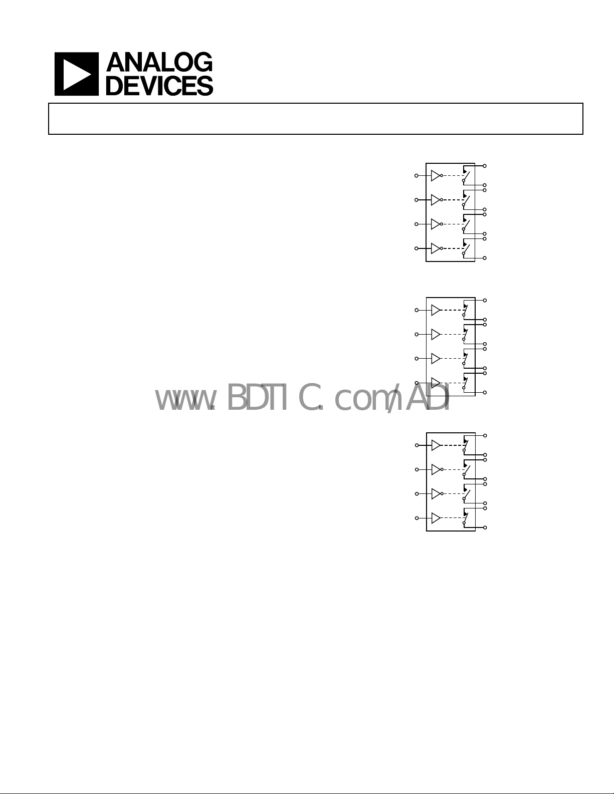
The ADG451/ADG452/ADG453 contain four independent,
gle-pole/single-throw (SPST) switches. The ADG451 and
sin
ADG452 differ only in that the digital control logic is inverted. The
ADG451 switches are turned on with a logic low on the appropriate
control input, while a logic high is required for the ADG452.
Rev. C
Information furnished by Analog Devices is believed to be accurate and reliable. However, no
responsibility is assumed by Anal og Devices for its use, nor for any infringements of patents or ot her
rights of third parties that may result from its use. Specifications subject to change without notice. No
license is granted by implication or otherwise under any patent or patent rights of Analog Devices.
Trademarks and registered trademarks are the property of their respective owners.
2
MOS process that
5 Ω RON SPST Switches
ADG451/ADG452/ADG453
FUNCTIONAL BLOCK DIAGRAMS
IN1
IN2
ADG451
IN3
IN4
WITCHES SHOWN FOR A LOGIC 1 INPUT.
Figure 1. ADG451
IN1
IN2
ADG452
IN3
IN4
SWITCHES SHOWN FOR A LOGIC 1 INPUT.
Figure 2. ADG452
IN1
IN2
ADG453
IN3
IN4
SWITCHES SHOWN FOR A LOGIC 1 INPUT.
Figure 3. ADG453
The ADG453 has two switches with digital control logic similar
to that of the ADG451, while the logic is inverted on the other
two switches.
Each switch conducts equally well in both
and each has an input signal range that extends to the supplies.
In the off condition, signal levels up to the supplies are blocked.
The ADG453 exhibits break-before-make switching action for
us
e in multiplexer applications. Inherent in the design is low
charge injection for minimum transients when switching the
digital inputs.
One Technology Way, P.O. Box 9106, Norwood, MA 02062-9106, U.S.A.
Tel: 781.329.4700 www.analog.com
Fax: 781.461.3113 ©2006 Analog Devices, Inc. All rights reserved.
S1
D1
S2
D2
S3
D3
S4
D4
05239-001
S1
D1
S2
D2
S3
D3
S4
D4
05239-101
S1
D1
S2
D2
S3
D3
S4
D4
05239-102
directions when on,

ADG451/ADG452/ADG453
www.BDTIC.com/ADI
TABLE OF CONTENTS
Features.............................................................................................. 1
Absolute Maximum Ratings ............................................................7
Applications....................................................................................... 1
General Description ......................................................................... 1
Functional Block Diagrams............................................................. 1
Revision History ............................................................................... 2
Product Highlights ........................................................................... 3
Specifications..................................................................................... 4
15 V Dual Supply.......................................................................... 4
12 V Single Supply........................................................................ 5
5 V Dual Supply............................................................................ 6
REVISION HISTORY
10/06—Rev. B to Rev. C
Changes to Table 4............................................................................ 9
Changes to Ordering Guide.......................................................... 18
12/04—Rev. A to Rev. B
pdated Format..................................................................Universal
U
Changes to Specifications Section.................................................. 3
Changes to Absolute Maximum Ratings Section......................... 8
Changes to Pin Configuration and Function
Descriptions Section ........................................................................ 9
Updated Outline Dimensions....................................................... 16
Changes to Ordering Guide.......................................................... 17
ESD Caution...................................................................................7
Pin Configuration and Function Descriptions..............................8
Typical Performance Characteristics..............................................9
Terminology.................................................................................... 11
Applications..................................................................................... 12
Test Circuits..................................................................................... 13
Outline Dimensions....................................................................... 15
Ordering Guide .......................................................................... 16
2/98—Rev. 0 to Rev. A
10/97—Revision 0: Initial Version
Rev. C | Page 2 of 16

ADG451/ADG452/ADG453
www.BDTIC.com/ADI
PRODUCT HIGHLIGHTS
1. Low RON (5 Ω maximum).
2. Ultralow Power Dissipation.
3. Extended Signal Range.
e ADG451/ADG452/ADG453 are fabricated on an enhanced
Th
2
LC
MOS process, giving an increased signal range that fully
extends to the supply rails.
4. Break-Before-Make Switching.
revents channel shorting when the switches are
This p
configured as a multiplexer (ADG453 only.)
5. Single-Supply Operation.
F
or applications in which the analog signal is unipolar, the
ADG451/ADG452/ADG453 can be operated from a single
rail power supply. The parts are fully specified with a single
12 V power supply and remain functional with single supplies
as low as 5.0 V.
6. Dual-Supply Operation.
or applications where the analog signal is bipolar, the
F
ADG451/ADG452/ADG453 can be operated from a dual
power supply ranging from ±4.5 V to ±20 V.
Rev. C | Page 3 of 16

ADG451/ADG452/ADG453
www.BDTIC.com/ADI
SPECIFICATIONS
15 V DUAL SUPPLY
VDD = 15 V, VSS = −15 V, VL = 5 V, GND = 0 V. All specifications T
Table 1.
B Version
Parameter 25°C T
ANALOG SWITCH
Analog Signal Range VSS to VDD V
On Resistance (RON) 4 Ω typ VD = −10 V to +10 V, IS = −10 mA
5 7 Ω max
On Resistance Match Between Channels (ΔRON) 0.1 Ω typ VD = ±10 V, IS = −10 mA
0.5 0.5 Ω max
On Resistance Flatness (R
) 0.2 Ω typ VD = −5 V, 0 V, +5 V, IS = −10 mA
FLAT(ON)
0.5 0.5 Ω max
LEAKAGE CURRENTS
2
Source Off Leakage, IS (OFF) ±0.02 nA typ VD = ±10 V, VS = ±10 V; see Figure 17
±0.5 ±2.5 nA max
Drain Off Leakage, ID (OFF) ±0.02 nA typ VD = ±10 V, VS = ±10 V; see Figure 17
±0.5 ±2.5 nA max
Channel On Leakage, ID, IS (ON) ±0.04 nA typ VD = VS = ±10 V; see Figure 18
±1 ±5 nA max
DIGITAL INPUTS
Input High Voltage, V
Input Low Voltage, V
Input Current, I
INL
2.4 V min
INH
0.8 V max
INL
or I
0.005 μA typ VIN = V
INH
±0.5 μA max
DYNAMIC CHARACTERISTICS
3
tON 70 ns typ RL = 300 Ω, CL = 35 pF, VS = ±10 V; see Figure 19
180 220 ns max
t
60 ns typ RL = 300 Ω, CL = 35 pF, VS = ±10 V; see Figure 19
OFF
140 180 ns max
Break-Before-Make Time Delay, tD (ADG453 Only) 15 ns typ RL = 300 Ω, CL = 35 pF, VS1 = VS2 = +10 V; see Figure 20
5 5 ns min
Charge Injection 20 pC typ VS = 0 V, RS = 0 Ω, CL = 1.0 nF; see Figure 21
30 pC max
Off Isolation 65 dB typ RL = 50 Ω, CL = 5 pF, f = 1 MHz; see Figure 22
Channel-to-Channel Crosstalk −90 dB typ
CS (OFF) 37 pF typ f = 1 MHz
CD (OFF) 37 pF typ f = 1 MHz
CD, CS (ON) 140 pF typ f = 1 MHz
POWER REQUIREMENTS VDD = 16.5 V, VSS = −16.5 V; digital inputs = 0 V or 5 V
IDD 0.0001 μA typ
0.5 5 μA max
ISS 0.0001 μA typ
0.5 5 μA max
IL 0.0001 μA typ
0.5 5 μA max
3
I
GND
0.0001 μA typ
0.5 5 μA max
1
Temperature range for B version is −40°C to +85°C.
2
T
= 70°C.
MAX
3
Guaranteed by design, not subject to production test.
MIN
1
to T
MIN
to T
MAX
, unless otherwise noted.
MAX
Unit Test Conditions/Comments
or V
INL
R
= 50 Ω, CL = 5 pF, f = 1 MHz; see Figure 23
L
; all others = 2.4 V or 0.8 V, respectively
INH
Rev. C | Page 4 of 16

ADG451/ADG452/ADG453
www.BDTIC.com/ADI
12 V SINGLE SUPPLY
VDD = 12 V, VSS = 0 V, VL = 5 V, GND = 0 V. All specifications T
Table 2.
B Version
Parameter 25°C T
ANALOG SWITCH
Analog Signal Range 0 V to VDD V
On Resistance (RON) 6 Ω typ VD = 0 V to +10 V, IS = −10 mA
8 10 Ω max
On Resistance Match Between Channels (ΔRON) 0.1 Ω typ VD = 10 V, IS = −10 mA
0.5 0.5 Ω max
On Resistance Flatness (R
LEAKAGE CURRENTS
2, 3
) 1.0 1.0 Ω typ VD = 0 V, 5 V, IS = −10 mA
FLAT(ON)
Source Off Leakage, IS (OFF) ±0.02 nA typ VD = 0 V, 10 V, VS = 0 V, 10 V; see Figure 17
±0.5 ±2.5 nA max
Drain Off Leakage, ID (OFF) ±0.02 nA typ VD = 0 V, 10 V, VS = 0 V, 10 V; see Figure 17
±0.5 ±2.5 nA max
Channel On Leakage, ID, IS (ON) ±0.04 nA typ VD = VS = 0 V, 10 V; see Figure 18
±1 ±5 nA max
DIGITAL INPUTS
Input High Voltage, V
Input Low Voltage, V
Input Current, I
INL
2.4 V min
INH
0.8 V max
INL
or I
0.005 μA typ VIN = V
INH
±0.5 μA max
DYNAMIC CHARACTERISTICS
4
tON 100 ns typ RL = 300 Ω, CL = 35 pF, VS = 8 V; see Figure 19
220 260 ns max
t
80 ns typ RL = 300 Ω, CL = 35 pF, VS = 8 V; see Figure 19
OFF
160 200 ns max
Break-Before-Make Time Delay, tD (ADG453 Only) 15 ns typ
10 10 ns min
Charge Injection 10 pC typ VS = 6 V, RS = 0 Ω, CL = 1.0 nF; see Figure 21
Channel-to-Channel Crosstalk −90 dB typ
CS (OFF) 60 pF typ f = 1 MHz
CD (OFF) 60 pF typ f = 1 MHz
CD, CS (ON) 100 pF typ f = 1 MHz
POWER REQUIREMENTS VDD = 13.2 V; digital inputs = 0 V or 5 V
IDD 0.0001 μA typ
0.5 5 μA max
IL 0.0001 μA typ
0.5 5 μA max VL = 5.5 V
4
I
GND
0.0001 μA typ
0.5 5 μA max VL = 5.5 V
1
Temperature range for B version is −40°C to +85°C.
2
T
= 70°C.
MAX
3
Tested with dual supplies.
4
Guaranteed by design, not subject to production test.
MIN
to T
MIN
, unless otherwise noted.
MAX
1
to T
Unit Test Conditions/Comments
MAX
or V
INH
INL
= 300 Ω, CL = 35 pF, VS1 = VS2 = 8 V;
R
L
see Figure 20
R
= 50 Ω, CL = 5 pF, f = 1 MHz; see Figure 23
L
Rev. C | Page 5 of 16
 Loading...