High Performance 4/8 Channel
S1
S8
A0
D
A1 A2 EN
ADG438F
1 OF 8
DECODER
A0
ADG439F
A1 EN
S1A
DA
S4A
S1B
S4B
DB
1 OF 4
DECODER
a
FEATURES
Fast Switching Times
t
250 ns max
ON
t
150 ns max
OFF
Fault and Overvoltage Protection (–40 V, +55 V)
All Switches OFF with Power Supply OFF
Analog Output of ON Channel Clamped Within Power
Supplies If an Overvoltage Occurs
Latch-Up Proof Construction
Break Before Make Construction
TTL and CMOS Compatible Inputs
APPLICATIONS
Data Acquisition Systems
Industrial and Process Control Systems
Avionics Test Equipment
Signal Routing Between Systems
High Reliability Control Systems
Fault-Protected Analog Multiplexers
ADG438F/ADG439F*
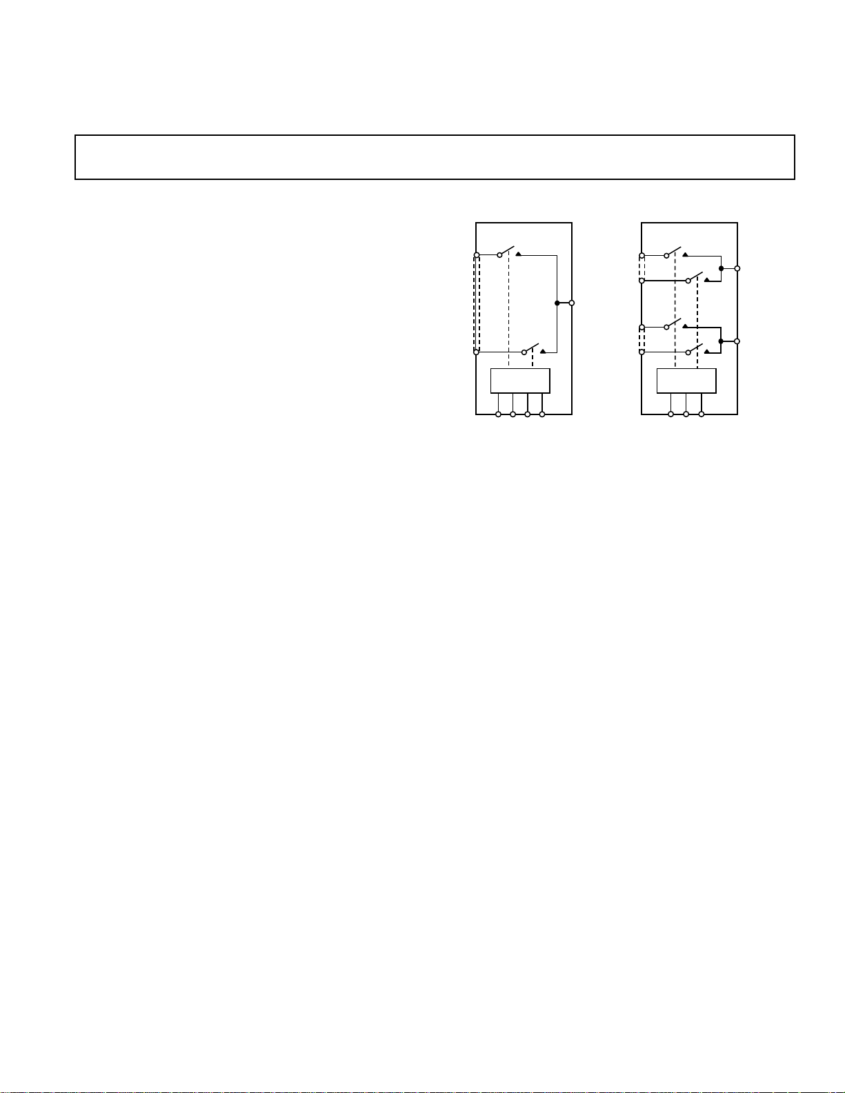
FUNCTIONAL BLOCK DIAGRAMS
GENERAL DESCRIPTION
The ADG438F/ADG439F are CMOS analog multiplexers, the
ADG438F comprising 8 single channels and the ADG439F
comprising four differential channels. These multiplexers provide fault protection. Using a series n-channel, p-channel, nchannel MOSFET structure, both device and signal source
protection is provided in the event of an overvoltage or power
loss. The multiplexer can withstand continuous overvoltage
inputs from –40 V to +55 V. During fault conditions, the multiplexer input (or output) appears as an open circuit and only a
few nanoamperes of leakage current will flow. This protects not
only the multiplexer and the circuitry driven by the multiplexer,
but also protects the sensors or signal sources which drive the
multiplexer.
The ADG438F switches one of eight inputs to a common output as determined by the 3-bit binary address lines A0, A1 and
A2. The ADG439F switches one of four differential inputs to a
common differential output as determined by the 2-bit binary
address lines A0 and A1. An EN input on each device is used to
enable or disable the device. When disabled, all channels are
switched OFF.
*Patent Pending.
REV. D
Information furnished by Analog Devices is believed to be accurate and
reliable. However, no responsibility is assumed by Analog Devices for its
use, nor for any infringements of patents or other rights of third parties
which may result from its use. No license is granted by implication or
otherwise under any patent or patent rights of Analog Devices.
PRODUCT HIGHLIGHTS
1. Fault Protection.
The ADG438F/ADG439F can withstand continuous voltage inputs up to –40 V or +55 V. When a fault occurs due
to the power supplies being turned off, all the channels
are turned off and only a leakage current of a few nanoamperes flows.
2. ON channel turns OFF while fault exists.
3. Low R
ON.
4. Fast Switching Times.
5. Break-Before-Make Switching.
Switches are guaranteed break-before-make so that input
signals are protected against momentary shorting.
6. Trench Isolation Eliminates Latch-up.
A dielectric trench separates the p- and n-channel MOSFETs
thereby preventing latch-up.
7. Improved OFF Isolation.
Trench isolation enhances the channel-to-channel isolation
of the ADG438F/ADG439F.
One Technology Way, P.O. Box 9106, Norwood, MA 02062-9106, U.S.A.
Tel: 781/329-4700 World Wide Web Site: http://www.analog.com
Fax: 781/326-8703 © Analog Devices, Inc., 2000

ADG438F/ADG439F–SPECIFICATIONS
1
Dual Supply
(V
= +15 V, V
DD
= –15 V, GND = 0 V, unless otherwise noted)
SS
B Version
–40ⴗC to –40ⴗC to
Parameter +25ⴗC +85ⴗC +105ⴗC Units Test Conditions/Comments
ANALOG SWITCH
Analog Signal Range V
R
ON
∆R
ON
R
Drift 0.6 %/°C typ V
ON
RON Match 3 3 3 % max V
+ 1.2 VSS + 1.2 V min
SS
VDD – 0.8 VDD – 0.8 V max
400 400 Ω max –10 V < V
5 5 % max –5 V < VS < +5 V, IS = 1 mA;
S
S
< +10 V, IS = 1 mA;
S
= 0 V, IS = 1 mA
= ±10 V, I
= 1 mA
S
LEAKAGE CURRENTS
Source OFF Leakage I
Drain OFF Leakage I
ADG438F ±0.5 ±5 ±30 nA max Test Circuit 3
(OFF) ±0.01 nA typ VD = ±10 V, V
S
(OFF) ±0.01 nA typ VD = ±10 V, V
D
±0.5 ±2 ±5 nA max Test Circuit 2
= ⫿10 V;
S
= ⫿10 V;
S
ADG439F ±0.5 ±5 ±15 nA max
Channel ON Leakage ID, I
ADG438F ±0.5 ±5 ±30 nA max Test Circuit 4
(ON) ±0.01 nA typ V
S
= V
S
= ±10 V;
D
ADG439F ±0.5 ±5 ±15 nA max
FAULT
Output Leakage Current ±0.02 nA typ V
(With Overvoltage) ±0.1 ±2 ±10 µA max
Input Leakage Current ±0.005 µA typ VS = ±25 V, V
(With Overvoltage) ±0.1 ±1 ±2 µA max
Input Leakage Current ±0.001 µA typ VS = ±25 V, V
(With Power Supplies OFF) ±0.1 ±1 ±4 µA max Test Circuit 6
= –33 V, +33 V or +50 V, VD = 0 V, Test Circuit 3
S
= ⫿10 V, Test Circuit 5
D
= VEN = A0, A1, A2 = 0 V
D
DIGITAL INPUTS
Input High Voltage, V
Input Low Voltage, V
Input Current
I
or I
INL
CIN, Digital Input Capacitance 5 pF typ
INH
DYNAMIC CHARACTERISTICS
t
TRANSITION
t
OPEN
t
(EN) 200 ns typ R
ON
t
(EN) 110 ns typ R
OFF
t
, Settling Time
SETT
0.1% 0.5 0.5 µs typ RL = 1 kΩ, C
INH
INL
2
170 ns typ R
220 300 320 ns max V
10 10 10 ns min R
250 300 300 ns max VS = +5 V; Test Circuit 9
150 180 180 ns max VS = +5 V; Test Circuit 9
0.01% 1.7 1.7 µs typ V
Charge Injection 4 pC typ VS =0V,R
OFF Isolation 80 dB typ R
Channel-to-Channel Crosstalk 85 dB typ R
2.4 2.4 V min
0.8 0.8 V max
±1 ±1 µA max V
= 0 or V
IN
= 1 MΩ, C
L
= ±10 V, V
S1
= 1 kΩ, C
L
VS = +5 V; Test Circuit 8
= 1 kΩ, C
L
= 1 kΩ, C
L
= +5 V
S
= 1 kΩ, C
L
VS = 7 V rms; Test Circuit 11
= 1 kΩ, C
L
VS = 7 V rms; Test Circuit 12
DD
= 35 pF;
L
= ⫿10 V; Test Circuit 7
S8
= 35 pF;
L
= 35 pF;
L
= 35 pF;
L
= 35 pF;
L
=0Ω,C
S
= 1 nF; Test Circuit 10
L
= 15 pF, f = 100 kHz;
L
= 15 pF, f = 100 kHz;
L
CS (OFF) 5 pF typ
CD (OFF)
ADG438F 50 pF typ
ADG439F 25 pF typ
POWER REQUIREMENTS
I
DD
I
SS
NOTES
1
Temperature range is as follows: B Version: –40°C to +105°C.
2
Guaranteed by design, not subject to production test.
Specifications subject to change without notice.
0.05 mA typ VIN = 0 V or 5 V
0.15 0.25 0.25 mA max
0.01 mA typ
0.02 0.04 0.04 mA max
–2– REV. D

ADG438F/ADG439F
ABSOLUTE MAXIMUM RATINGS*
(T
= +25°C unless otherwise noted)
A
VDD to VSS . . . . . . . . . . . . . . . . . . . . . . . . . . . . . . . . . . .+44 V
to GND . . . . . . . . . . . . . . . . . . . . . . . . . . –0.3 V to +25 V
V
DD
to GND . . . . . . . . . . . . . . . . . . . . . . . . . . . +0.3 V to –25 V
V
SS
, VA Digital Input . . . . . . . – 0.3 V to VDD + 2 V or 20 mA,
V
EN
Whichever Occurs First
, Analog Input Overvoltage with Power ON . . . . . VSS – 25 V
V
S
, Analog Input Overvoltage with Power OFF
V
S
to V
+ 40 V
DD
. . . . . . . . . . . . . . . . . . . . . . . . . . . . . . . . . . . .–40 V to +55 V
Continuous Current, S or D . . . . . . . . . . . . . . . . . . . . . 20 mA
Peak Current, S or D
(Pulsed at 1 ms, 10% Duty Cycle max) . . . . . . . . . . . 40 mA
Operating Temperature Range
Industrial (B Version) . . . . . . . . . . . . . . . . –40°C to +105°C
Storage Temperature Range . . . . . . . . . . . . . –65°C to +150°C
Junction Temperature . . . . . . . . . . . . . . . . . . . . . . . . . +150°C
Plastic Package
, Thermal Impedance . . . . . . . . . . . . . . . . . . . . 117°C/W
θ
JA
Lead Temperature, Soldering (10 sec) . . . . . . . . . . . +260°C
SOIC Package
, Thermal Impedance
θ
JA
Narrow Body . . . . . . . . . . . . . . . . . . . . . . . . . . . 125°C/W
Wide Body . . . . . . . . . . . . . . . . . . . . . . . . . . . . . . 90°C/W
Lead Temperature, Soldering
Vapor Phase (60 sec) . . . . . . . . . . . . . . . . . . . . . . +215°C
Infrared (15 sec) . . . . . . . . . . . . . . . . . . . . . . . . . . +220°C
*Stresses above those listed under Absolute Maximum Ratings may cause perma-
nent damage to the device. This is a stress rating only; functional operation of the
device at these or any other conditions above those listed in the operational
sections of this specification is not implied. Exposure to absolute maximum rating
conditions for extended periods may affect device reliability. Only one absolute
maximum rating may be applied at any one time.
ORDERING GUIDE
Model Temperature Range Package Option*
ADG438FBN –40°C to +105°C N-16
ADG438FBR –40°C to +105°C R-16N
ADG439FBN –40°C to +105°C N-16
ADG439FBR –40°C to +105°C R-16N
ADG439FBRW –40°C to +105°C R-16W
*N = Plastic DIP; R-16N = 0.15" Small Outline IC (SOIC); R-16W = 0.3"
Small Outline IC (SOIC).
Table I. ADG438F Truth Table
A2 A1 A0 EN ON SWITCH
XXX0 NONE
00011
00112
01013
01114
10015
10116
11017
11118
X = Don’t Care
Table II. ADG439F Truth Table
A1 A0 EN ON SWITCH PAIR
X X 0 NONE
0011
0112
1013
1114
X = Don’t Care
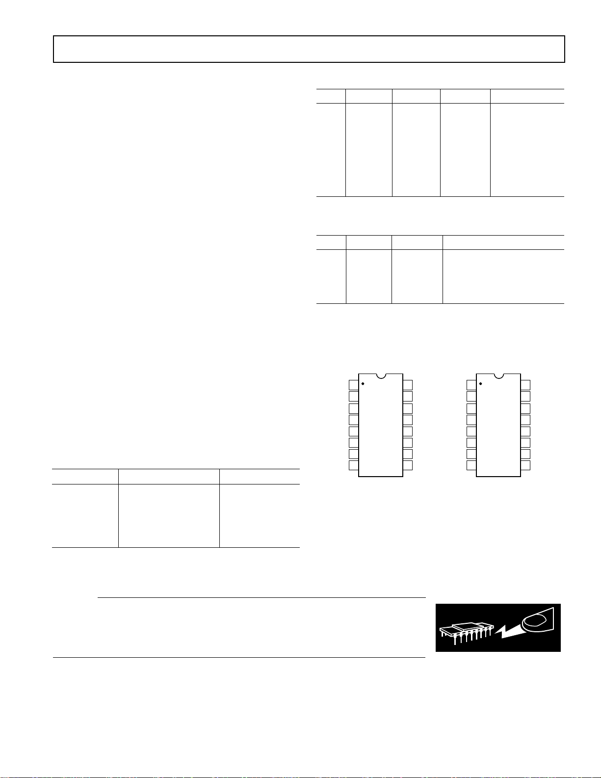
ADG438F/ADG439F PIN CONFIGURATIONS
DIP/SOIC DIP/SOIC
1
A0
2
EN
3
V
SS
ADG438F
4
S1
TOP VIEW
5
S2
(Not to Scale)
S3
6
7
S4
DS8
89
16
A1
15
A2
GND
14
V
13
DD
S5
12
S6
11
S7
10
1
A0
2
EN
V
3
SS
4
S1A
5
S2A
6
S3A
7
S4A
89
DA
ADG439F
TOP VIEW
(Not to Scale)
16
A1
15
GND
14
V
DD
S1B
13
12
S2B
11
S3B
10
S4B
DB
CAUTION
ESD (electrostatic discharge) sensitive device. Electrostatic charges as high as 4000 V readily
accumulate on the human body and test equipment and can discharge without detection.
Although the ADG438F/ADG439F features proprietary ESD protection circuitry, permanent
damage may occur on devices subjected to high energy electrostatic discharges. Therefore, proper
ESD precautions are recommended to avoid performance degradation or loss of functionality.
–3–REV. D
WARNING!
ESD SENSITIVE DEVICE
 Loading...