Analog Devices ADG417 Datasheet

LC2MOS Precision
ADG417
IN
D
S
SWITCH SHOWN FOR A
LOGIC "1" INPUT
a
FEATURES
44 V Supply Maximum Ratings
V
to VDD Analog Signal Range
SS
Low On Resistance (<35 ⍀)
Ultralow Power Dissipation (<35 W)
Fast Switching Times
t
(160 ns max)
ON
t
(100 ns max)
OFF
Break-Before-Make Switching Action
Plug-In Replacement for DG417
APPLICATIONS
Precision Test Equipment
Precision Instrumentation
Battery Powered Systems
Sample Hold Systems
GENERAL DESCRIPTION
The ADG417 is a monolithic CMOS SPST switch. This switch
is designed on an enhanced LC
power dissipation yet gives high switching speed, low on resistance and low leakage currents.
The on resistance profile of the ADG417 is very flat over the
full analog input range ensuring excellent linearity and low
distortion. The part also exhibits high switching speed and high
signal bandwidth. CMOS construction ensures ultralow power
dissipation making the parts ideally suited for portable and
battery powered instruments.
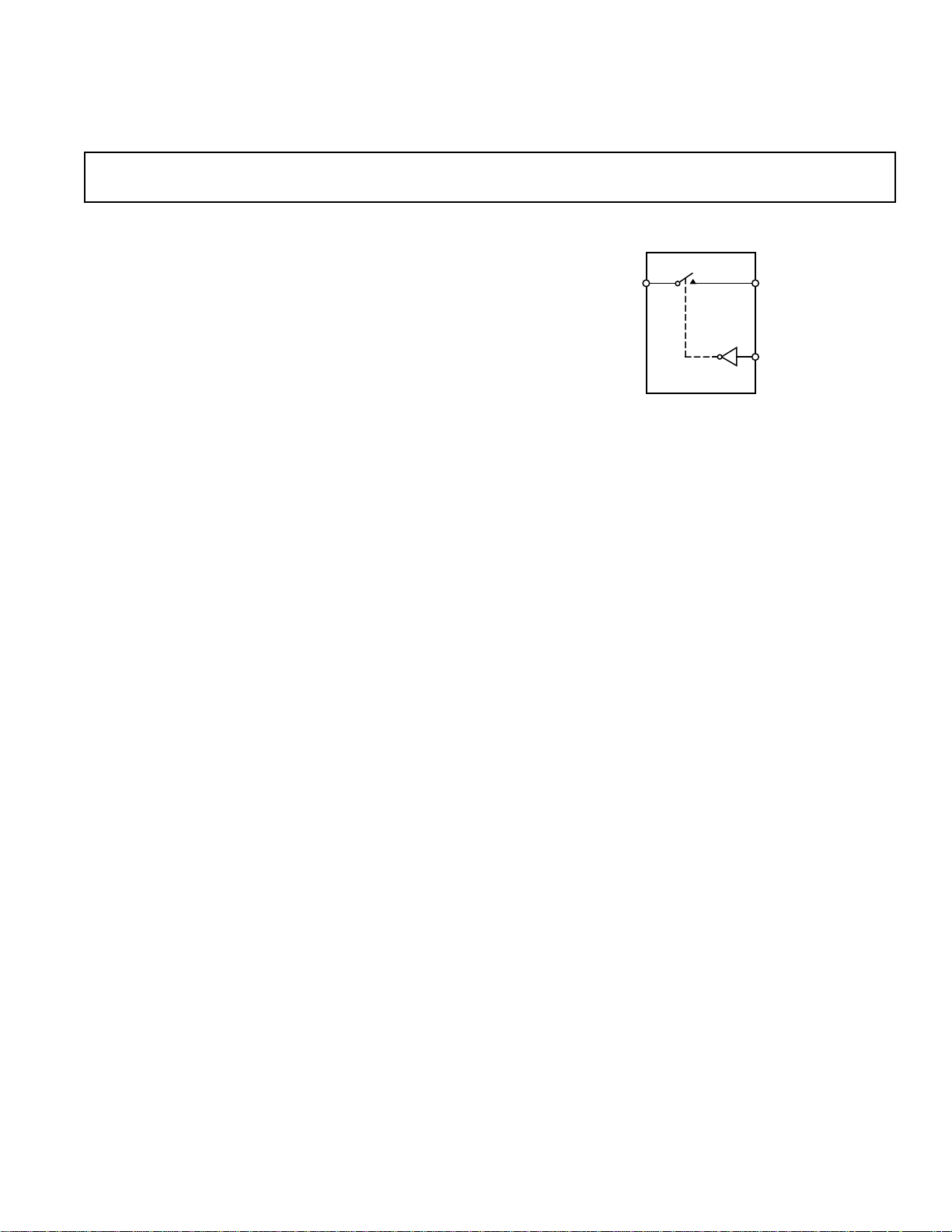
The ADG417 switch, which is turned ON with a logic low on
the control input, conducts equally well in both directions when
ON and has an input signal range that extends to the supplies.
In the OFF condition, signal levels up to the supplies are
blocked. The ADG417 exhibits break-before-make switching
action for use in multiplexer applications. Inherent in the design
is low charge injection for minimum transients when switching
the digital input.
2
MOS process that provides low
Mini-DIP Analog Switch
ADG417
FUNCTIONAL BLOCK DIAGRAM
PRODUCT HIGHLIGHTS
1. Extended Signal Range
The ADG417 is fabricated on an enhanced LC
giving an increased signal range that extends to the supply
rails.
2. Ultralow Power Dissipation
3. Low R
4. Single Supply Operation
ON
For applications where the analog signal is unipolar, the
ADG417 can be operated from a single rail power supply.
The part is fully specified with a single +12 V power supply
and will remain functional with single supplies as low as
+5 V.
2
MOS process,
REV. A
Information furnished by Analog Devices is believed to be accurate and
reliable. However, no responsibility is assumed by Analog Devices for its
use, nor for any infringements of patents or other rights of third parties
which may result from its use. No license is granted by implication or
otherwise under any patent or patent rights of Analog Devices.
One Technology Way, P.O. Box 9106, Norwood, MA 02062-9106, U.S.A.
Tel: 781/329-4700 World Wide Web Site: http://www.analog.com
Fax: 781/326-8703 © Analog Devices, Inc., 1998

ADG417–SPECIFICATIONS
1
(V
Dual Supply
= +15 V ⴞ 10%, V
DD
Parameter +25ⴗC +85ⴗC +25ⴗC +125ⴗC Units Test Conditions/Comments
ANALOG SWITCH
Analog Signal Range V
R
ON
LEAKAGE CURRENTS V
Source OFF Leakage I
Drain OFF Leakage I
Channel ON Leakage I
(OFF) ±0.1 ±0.1 nA typ VD = ±15.5 V, V
S
(OFF) ±0.1 ±0.1 nA typ VD = ±15.5 V, V
D
, I
(ON) ±0.1 ±0.1 nA typ V
D
S
DIGITAL INPUTS
Input High Voltage, V
Input Low Voltage, V
INH
INL
Input Current
I
or I
INL
INH
DYNAMIC CHARACTERISTICS
t
ON
t
OFF
2
Charge Injection 7 7 pC typ V
OFF Isolation 80 80 dB typ R
C
(OFF) 6 6 pF typ
S
C
(OFF) 6 6 pF typ
D
CD, CS (ON) 55 55 pF typ
POWER REQUIREMENTS V
I
DD
I
SS
I
L
NOTES
1
Temperature ranges are as follows: B Version: –40°C to +85°C; T Version: –55°C to +125°C.
2
Guaranteed by design, not subject to production test.
Specifications subject to change without notice.
= –15 V ⴞ 10%, VL = +5 V ⴞ 10%, GND = 0 V, unless otherwise noted)
SS
B Version T Version
–40ⴗC to –55ⴗC to
SS
to V
DD
VSS to V
DD
V
25 25 Ω typ VD = ±12.5 V, I
35 45 35 45 Ω max V
= +13.5 V, VSS = –13.5 V
DD
= +16.5 V, VSS = –16.5 V
DD
±0.25 ±5 ±0.25 ±15 nA max Test Circuit 2
±0.25 ±5 ±0.25 ±15 nA max Test Circuit 2
= V
= ±15.5 V;
S
D
±0.4 ±5 ±0.4 ±30 nA max Test Circuit 3
2.4 2.4 V min
0.8 0.8 V max
±0.005 ±0.005 µA typ V
IN
= V
INL
or V
±0.5 ±0.5 µA max
100 100 ns typ R
160 200 145 200 ns max V
60 60 ns typ R
100 150 100 150 ns max V
= 300 Ω, C
L
= ±10 V; Test Circuit 4
S
= 300 Ω, C
L
= ±10 V; Test Circuit 4
S
= 0 V, R
S
C
= 10 nF; Test Circuit 5
L
= 50 Ω, f = 1 MHz;
L
= 0 Ω,
L
Test Circuit 6
= +16.5 V, VSS = –16.5 V
0.0001 0.0001 µA typ V
DD
= 0 V or 5 V
IN
1 2.5 1 2.5 µA max
0.0001 0.0001 µA typ
1 2.5 1 2.5 µA max
0.0001 0.0001 µA typ V
= +5.5 V
L
1 2.5 1 2.5 µA max
= –10 mA
S
= ⫿15.5 V;
S
= ⫿15.5 V;
S
INH
= 35 pF;
L
= 35 pF;
L
–2–
REV. A

ADG417
TOP VIEW
(Not to Scale)
8
7
6
5
1
2
3
4
S
NC
GND
D
V
SS
IN
V
L
V
DD
ADG417
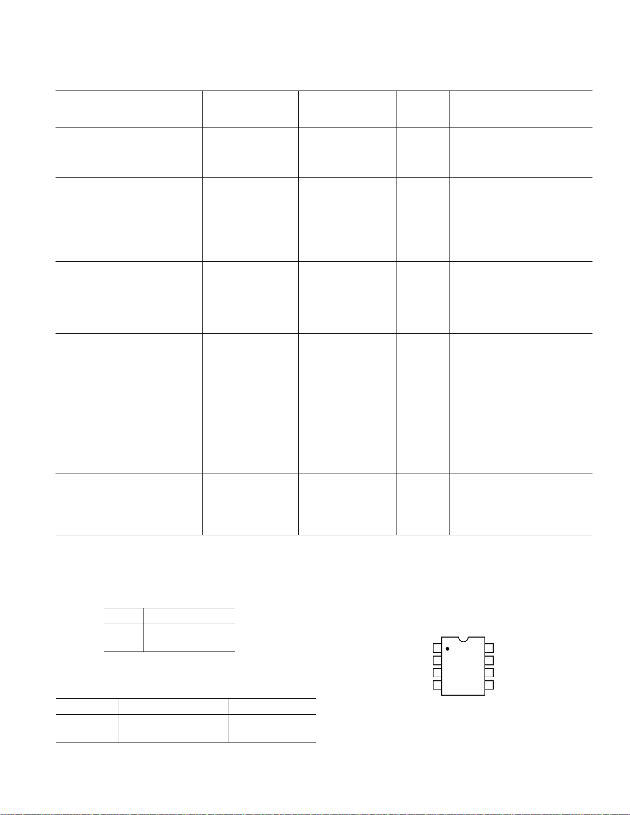
NC = NO CONNECT
Single Supply
Parameter +25ⴗC +85ⴗC +25ⴗC +125ⴗC Units Test Conditions/Comments
ANALOG SWITCH
Analog Signal Range 0 to V
R
ON
LEAKAGE CURRENT V
Source OFF Leakage I
Drain OFF Leakage I
Channel ON Leakage I
DIGITAL INPUTS
Input High Voltage, V
Input Low Voltage, V
Input Current
I
or I
INL
INH
DYNAMIC CHARACTERISTICS
t
ON
t
OFF
Charge Injection 11 11 pC typ V
OFF Isolation 80 80 dB typ R
C
(OFF) 13 13 pF typ
S
C
(OFF) 13 13 pF typ
D
CD, CS (ON) 65 65 pF typ
POWER REQUIREMENTS V
I
DD
I
L
NOTES
1
Temperature ranges are as follows: B Version: –40°C to +85°C; T Version: –55°C to +125°C.
2
Guaranteed by design, not subject to production test.
Specifications subject to change without notice.
1
(V
= +12 V ⴞ 10%, V
DD
(OFF) ±0.1 ±0.1 nA typ V
S
(OFF) ±0.1 ±0.1 nA typ V
D
, I
(ON) ±0.1 ±0.1 nA typ V
D
S
INH
INL
2
= 0 V, VL = +5 V ⴞ 10%, GND = 0 V, unless otherwise noted)
SS
B Version T Version
–40ⴗC to –55ⴗC to
DD
0 to V
DD
V
40 40 Ω typ V
60 70 Ω max V
±0.25 ±5 ±0.25 ±15 nA max Test Circuit 2
±0.25 ±5 ±0.25 ±15 nA max Test Circuit 2
±0.4 ±5 ±0.4 ±30 nA max Test Circuit 3
2.4 2.4 V min
0.8 0.8 V max
±0.005 ±0.005 µA typ V
±0.5 ±0.5 µA max
180 250 180 250 ns max R
85 110 85 110 ns max R
0.0001 0.0001 µA typ V
12.5 12.5 µA max
0.0001 0.0001 µA typ V
12.5 12.5 µA max
= +3 V, +8.5 V, IS = –10 mA
D
= +10.8 V
DD
= +13.2 V
DD
= 12.2 V/1 V, VS = 1 V/12.2 V;
D
= 12.2 V/1 V, VS = 1 V/12.2 V;
D
= VD = 12.2 V/1 V;
S
= V
INL
or V
= 0 Ω,
S
INH
= 35 pF;
L
= 35 pF;
L
IN
= 300 Ω, C
L
V
= +8 V; Test Circuit 4
S
= 300 Ω, C
L
V
= +8 V; Test Circuit 4
S
= 0 V, R
S
C
= 10 nF; Test Circuit 5
L
= 50 Ω, f = 1 MHz;
L
Test Circuit 6
= +13.2 V
DD
= 0 V or 5 V
IN
= +5.5 V
L
Table I. Truth Table
Logic Switch Condition
0ON
1 OFF
ORDERING GUIDE
Model Temperature Range Package Options*
ADG417BN –40°C to +85°C N-8
ADG417BR –40°C to +85°C SO-8
*N = Plastic DIP, SO = 0.15" Small Outline IC (SOIC).
REV. A –3–
PIN CONFIGURATION
DIP/SOIC
 Loading...