

LC2MOS
FEATURES
44 V supply maximum ratings
±15 V analog signal range
Low on resistance (< 35 Ω)
Ultralow power dissipation (35 µW)
Fast switching times
t
< 175 ns
ON
t
< 145 ns
OFF
TTL-/CMOS-compatible
Plug-in replacement for DG411/DG412/DG413
APPLICATIONS
Audio and video switching
Automatic test equipment
Precision data acquisition
Battery-powered systems
Sample-and-hold systems
Communication systems
GENERAL DESCRIPTION
The ADG411, ADG412, and ADG413 are monolithic CMOS
devices comprising four independently selectable switches.
They are designed on an enhanced LC
provides low power dissipation yet gives high switching speed
and low on resistance.
The on resistance profile is very flat over the full analog input
range ensuring excellent linearity and low distortion when
switching audio signals. Fast switching speed coupled with high
signal bandwidth also make the parts suitable for video signal
switching. CMOS construction ensures ultralow power
dissipation, making the parts ideally suited for portable and
battery-powered instruments.
2
MOS process which
Precision Quad SPST Switches
ADG411/ADG412/ADG413
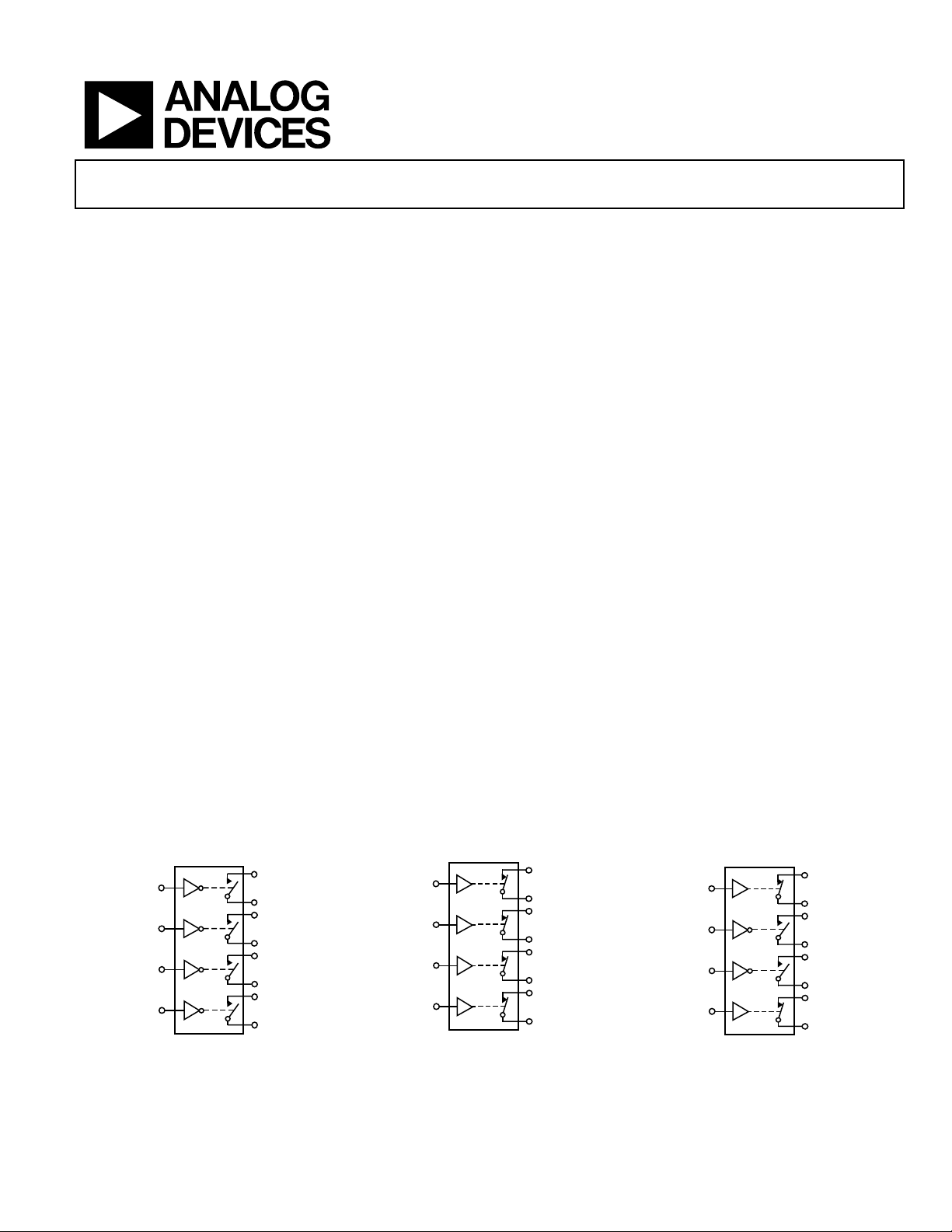
The ADG411, ADG412, and ADG413 contain four independent
SPST switches. The ADG411 and ADG412 differ only in that
the digital control logic is inverted. The ADG411 switches are
turned on with a logic low on the appropriate control input,
while a logic high is required for the ADG412. The ADG413
has two switches with digital control logic similar to that of the
ADG411 while the logic is inverted on the other two switches.
Each switch conducts equally well in both directions when on,
and each has an input signal range that extends to the supplies.
In the off condition, signal levels up to the supplies are blocked.
All switches exhibit break-before-make switching action for use
in multiplexer applications. Inherent in the design is low charge
injection for minimum transients when switching the digital
inputs.
PRODUCT HIGHLIGHTS
1. Extended signal range
The ADG411, ADG412, and ADG413 are fabricated on an
enhanced LC
extends fully to the supply rails.
2. Ultralow power dissipation
3. Low R
4. Break-before-make switching
This prevents channel shorting when the switches are
configured as a multiplexer.
5. Single-supply operation
For applications where the analog signal is unipolar, the
ADG411, ADG412, and ADG413 can be operated from a
single-rail power supply. The parts are fully specified with a
single 12 V power supply and remain functional with single
supplies as low as 5 V.
2
MOS, giving an increased signal range which
ON
FUNCTIONAL BLOCK DIAGRAMS
IN1
IN2
ADG411
IN3
IN4
SWITCHES SHOWN FOR A LOGIC 1 INPUT
Rev. C
Information furnished by Analog Devices is believed to be accurate and reliable.
However, no responsibility is assumed by Analog Devices for its use, nor for any
infringements of patents or other rights of third parties that may result from its use.
Specifications subject to change without notice. No license is granted by implication
or otherwise under any patent or patent rights of Analog Devices. Trademarks and
registered trademarks are the property of their respective owners.
Figure 1. ADG411
S1
D1
S2
D2
S3
D3
S4
D4
00024-001
IN1
IN2
IN3
IN4
SWITCHES SHOWN FOR A LOGIC 1 INPUT
Figure 2. ADG412
ADG412
S1
D1
S2
D2
S3
D3
S4
D4
00024-002
One Technology Way, P.O. Box 9106, Norwood, MA 02062-9106, U.S.A.
Tel: 781.329.4700
Fax: 781.326.8703 © 2004 Analog Devices, Inc. All rights reserved.
www.analog.com
IN1
IN2
ADG413
IN3
IN4
SWITCHES SHOWN FOR A LOGIC 1 INPUT
Figure 3. ADG413
S1
D1
S2
D2
S3
D3
S4
D4
00024-003

ADG411/ADG412/ADG413
TABLE OF CONTENTS
Specifications..................................................................................... 3
Typical Perfor m a n c e C haracter i s t ic s ..............................................7
Dual Supply ................................................................................... 3
Single Supply ................................................................................. 4
Absolute Maximum Ratings............................................................ 5
ESD Caution.................................................................................. 5
Pin Configurations and Function Descriptions ........................... 6
REVISION HISTORY
11/04—Rev. B to Rev. C
Format Updated..................................................................Universal
Change to Package Drawing (Figure 23)..................................... 13
Changes to Ordering Guide.......................................................... 14
7/04—Rev. A to Rev. B
Changes to ORDERING GUIDE .....................................................5
Updated OUTLINE DIMENSIONS ...............................................11
Te r mi n ol o g y .......................................................................................9
Applications..................................................................................... 10
Test C ir c uit s ..................................................................................... 11
Outline Dimensions ....................................................................... 13
Ordering Guide .......................................................................... 14
Rev. C | Page 2 of 16
ADG411/ADG412/ADG413
SPECIFICATIONS
DUAL SUPPLY
VDD = 15 V ± 10%, VSS = –15 V ± 10%, VL = 5 V ± 10%, GND = 0 V, unless otherwise noted.
Table 1.
B Version T Version
Parameter +25°C −40°C to +85°C +25°C −55°C to +125°C Unit Test Conditions/Comments
ANALOG SWITCH
Analog Signal Range VDD to V
R
ON
25 25 Ω typ VD = ±8.5 V, IS = −10 mA;
SS
V
DD
to V
SS
35 45 35 45 Ω max VDD = +13.5 V, VSS = −13.5 V
LEAKAGE CURRENTS
Source OFF Leakage IS (OFF) ±0.1 ±0.1 nA typ
±0.25 ±0.25 ±0.25 ±20 nA max Figure 15
Drain OFF Leakage ID (OFF) ±0.1 ±0.1 nA typ
±0.25 ±5 ±0.25 ±20 nA max Figure 15
Channel ON Leakage ID, IS (ON) ±0.1 ±0.1 nA typ VD = VS = +15.5 V/−15.5 V;
±0.4 ±10 ±0.4 ± 40 nA max Figure 16
DIGITAL INPUTS
Input High Voltage, V
Input Low Voltage, V
INH
INL
2.4 2.4 V min
0.8 0.8 V max
Input Current
I
or I
INL
INH
0.005 0.005 µA typ VIN = V
±0.5 ±0.5 µA max
DYNAMIC CHARACTERISTICS
t
ON
2
110 110 ns typ RL = 300 Ω, CL = 35 pF;
175 175 ns max VS = ±10 V; Figure 17
t
OFF
100 100 ns typ RL = 300 Ω, CL = 35 pF;
145 145 ns max VS = ±10 V; Figure 17
Break-Before-Make Time Delay,
(ADG413 Only)
t
D
25 25 ns typ
Charge Injection 5 5 pC typ
OFF Isolation 68 68 dB typ
Channel-to-Channel Crosstalk 85 85 dB typ
CS (OFF) 9 9 pF typ f = 1 MHz
CD (OFF) 9 9 pF typ f = 1 MHz
CD, CS (ON) 35 35 pF typ f = 1 MHz
POWER REQUIREMENTS
I
DD
0.0001 0.0001 µA typ
1 5 1 5 µA max
I
SS
0.0001 0.0001 µA typ
1 5 1 5 µA max
I
L
0.0001 0.0001 µA typ
1 5 1 5 µA max
1
Temperature ranges are as follows: B versions: −40°C to +85°C; T versions: −55°C to +125°C.
2
Guaranteed by design; not subject to production test.
1
V
VDD = +16.5 V, VSS = −16.5 V
= +15.5 V/−15.5 V,
V
D
V
= −15.5 V/+15.5 V;
S
= +15.5 V/−15.5 V,
V
D
= −15.5 V/+15.5 V;
V
S
or V
INL
INH
= 300 Ω, CL = 35 pF;
R
L
= VS2 = 10 V; Figure 18
V
S1
= 0 V, RS = 0 Ω, CL = 10 nF;
V
S
Figure 19
= 50 Ω, CL = 5 pF, f = 1 MHz;
R
L
Figure 20
= 50 Ω, CL = 5 pF, f = 1 MHz;
R
L
Figure 21
= +16.5 V, VSS = −16.5 V;
V
DD
Digital inputs = 0 V or 5 V
Rev. C | Page 3 of 16
ADG411/ADG412/ADG413
SINGLE SUPPLY
VDD = 12 V ± 10%, VSS = 0 V, VL = 5 V ± 10%, GND = 0 V, unless otherwise noted.
Table 2.
B Version T Version
Parameter +25°C −40°C to + 85°C +25°C −55°C to +125°C Unit Test Conditions/Comments
ANALOG SIGNAL RANGE 0 V to V
R
ON
40 40 Ω typ 0 < VD = 8.5 V, IS = −10 mA;
DD
0 V to V
80 100 80 100 Ω max VDD = 10.8 V
LEAKAGE CURRENTS VDD = 13.2 V
Source OFF Leakage IS (OFF) ±0.1 ±0.1 nA typ VD = 12.2 V/1 V, VS = 1 V/12.2 V;
±0.25 ±5 ±0.25 ±20 nA max Figure 15
Drain OFF Leakage ID (OFF) ±0.1 ±0.1 nA typ VD = 12.2 V/1 V, VS = 1 V/12.2 V;
±0.25 ±5 ±0.25 ±20 nA max Figure 15
Channel ON Leakage ID, IS (ON) ±0.1 ±0.1 nA typ VD = VS = 12.2 V/1 V;
±0.4 ±10 ±0.4 ±40 nA max Figure 16
DIGITAL INPUTS
Input High Voltage, V
Input Low Voltage, V
INH
INL
2.4 2.4 V min
0.8 0.8 V max
Input Current
I
or I
INL
INH
0.005 0.005 µA typ VIN = V
±0.5 ±0.5 µA max
DYNAMIC CHARACTERISTICS
t
ON
2
175 175 ns typ RL = 300 Ω, CL = 35 pF;
250 250 ns max VS = 8 V; Figure 17
t
OFF
95 95 ns typ RL = 300 Ω, CL = 35 pF;
125 125 ns max VS = 8 V; Figure 17
Break-Before-Make Time
Delay, t
(ADG413 Only)
D
25 25 ns typ
Charge Injection 25 25 pC typ
OFF Isolation 68 68 dB typ
Channel-to-Channel Crosstalk 85 85 dB typ
CS (OFF) 9 9 pF typ f = 1 MHz
CD (OFF) 9 9 pF typ f = 1 MHz
CD, CS (ON) 35 35 pF typ f = 1 MHz
POWER REQUIREMENTS
I
DD
0.0001 0.0001 µA typ
1 5 1 5 µA max
I
L
0.0001 0.0001 µA typ
1 5 1 5 µA max VL = 5.25 V
1
Temperature ranges are as follows: B versions:−40°C to +85°C; T versions: −55°C to +125°C.
2
Guaranteed by design; not subject to production test.
Table 3. Truth Table (ADG411/ADG412)
ADG411 In ADG412 In Switch Condition
0 1 ON
1 0 OFF
Table 4. Truth Table (ADG413)
Logic Switch 1, 4 Switch 2, 3
0 OFF ON
1 ON OFF
1
DD
V
INL
= 300 Ω, CL = 35 pF;
R
L
= VS2 = +10 V; Figure 18
V
S1
= 0 V, RS = 0 Ω, CL = 10 nF;
V
S
or V
INH
Figure 19
= 50 Ω, CL = 5 pF, f = 1 MHz;
R
L
Figure 20
= 50 Ω, CL = 5 pF, f = 1 MHz;
R
L
Figure 21
= 13.2 V;
V
DD
Digital inputs = 0 V or 5 V
Rev. C | Page 4 of 16
ADG411/ADG412/ADG413
ABSOLUTE MAXIMUM RATINGS
TA = 25°C, unless otherwise noted.
Table 5.
Parameters Ratings
VDD to V
SS
VDD to GND −0.3 V to +25 V
VSS to GND +0.3 V to −25 V
VL to GND −0.3 V to VDD + 0.3 V
Analog, Digital Inputs
Continuous Current, S or D 30 mA
Peak Current, S or D (Pulsed at 1 ms,
10% Duty Cycle max)
Operating Temperature Range
Industrial (B Version) −40°C to +85°C
Extended (T Version) −55°C to +125°C
Storage Temperature Range −65°C to +150°C
Junction Temperature 150°C
CERDIP Package, Power Dissipation 900 mW
θJA Thermal Impedance 76°C/W
Lead Temperature, Soldering (10 s) 300°C
PDIP, Power Dissipation 470 mW
θJA Thermal Impedance 117°C/W
Lead Temperature, Soldering (10 s) 260°C
SOIC Package, Power Dissipation 600 mW
θJA Thermal Impedance 77°C/W
TSSOP Package, Power Dissipation 450 mW
θJA Thermal Impedance 115°C/W
θJC Thermal Impedance 35°C/W
Lead Temperature, Soldering
Vapor Phase (60 s) 215°C
Infrared (15 s) 220°C
________________________________________
1
Overvoltages at IN, S, or D are clamped by internal diodes. Current should
be limited to the maximum ratings given.
1
44 V
VSS − 2 V to VDD + 2 V or
30 mA, whichever
occurs first
100 mA
Stresses above those listed under Absolute Maximum Ratings
may cause permanent damage to the device. This is a stress
rating only; functional operation of the device at these or any
other conditions above those listed in the operational sections
of this specification is not implied. Exposure to absolute
maximum rating conditions for extended periods may affect
device reliability. Only one absolute maximum rating may be
applied at any one time.
ESD CAUTION
ESD (electrostatic discharge) sensitive device. Electrostatic charges as high as 4000 V readily accumulate on
the human body and test equipment and can discharge without detection. Although this product features
proprietary ESD protection circuitry, permanent damage may occur on devices subjected to high energy
electrostatic discharges. Therefore, proper ESD precautions are recommended to avoid performance
degradation or loss of functionality.
Rev. C | Page 5 of 16

ADG411/ADG412/ADG413
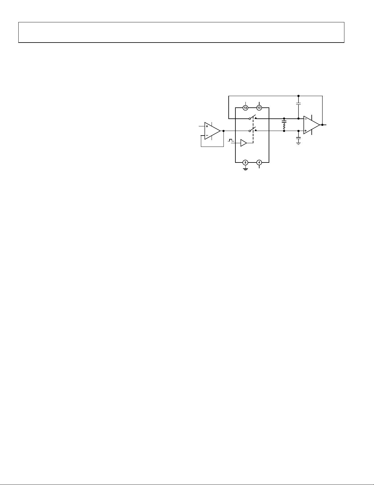
PIN CONFIGURATION AND FUNCTION DESCRIPTIONS
IN1
V
GND
IN4
D1
S1
SS
S4
D4
1
2
ADG411/
3
ADG412/
ADG413
4
TOP VIEW
5
(Not to Scale)
6
7
8
16
IN2
15
D2
14
S2
13
V
DD
12
V
L
11
S3
10
D3
9
IN3
Figure 4. Pin Configuration
Table 6. Pin Function Descriptions
Pin No. Mnemonic Description
1, 8, 9, 16 IN1–IN4 Logic Control Input.
2, 7, 10, 15 D1–D4 Drain Terminal. Can be an input or output.
3, 6, 11, 14 S1–S4 Source Terminal. Can be an input or output.
4 V
SS
Most Negative Power Supply Potential in Dual Supplies. In single supply applications, it may be
connected to GND.
5 GND Ground (0 V) Reference.
12 V
13 V
L
DD
Logic Power Supply (5 V).
Most Positive Power Supply Potential.
00024-004
Rev. C | Page 6 of 16
ADG411/ADG412/ADG413
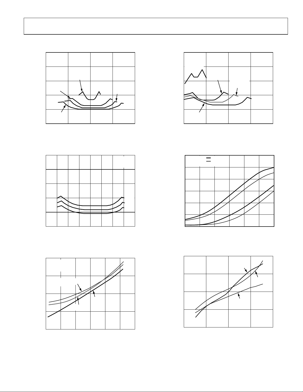
TYPICAL PERFORMANCE CHARACTERISTICS
50
40
V
= +5V
DD
= –5V
V
30
V
= +10V
(Ω)
ON
R
DD
V
= –10V
SS
20
SS
V
V
T
A
V
L
DD
SS
= 25°C
= +5V
= +12V
= –12V
50
VDD = +5V
40
V
= 0V
SS
V
= +10V
DD
= 0V
V
30
)
Ω
(
ON
R
20
SS
V
V
DD
SS
= +12V
= 0V
T
A
V
L
= 25°C
= +5V
10
V
= +15V
DD
= –15V
V
SS
0
–20 20
Figure 5. On Resistance as a Function of V
VD OR VS– DRAIN OR SOURCE VOLTAGE (V)
D
50
40
30
(Ω)
ON
R
20
10
0
–20 –15 –10 –5 0 5 10 15 20
Figure 6. On Resistance as a Function of V
VD OR VS– DRAIN OR SOURCE VOLTAGE (V)
(VS) for Different Temperatures
D
10
VDD = +15V
V
= –15V
SS
= +5V
V
L
1
= ±15V
V
0.1
0.01
LEAKAGE CURRENT (nA)
D
V
S
= ±15V
I
S
(OFF)
(ON)
I
D
ID (OFF)
100–10
(VS) Dual Supplies
VDD = +15V
= –15V
V
SS
V
= +5V
L
125°C
85°C
25°C
00024-005
00024-006
10
= +15V
V
DD
= 0V
V
SS
0
02
VD OR VS– DRAIN OR SOURCE VOLTAGE (V)
Figure 8. On Resistance as a Function of V
15105
(VS) Single Supply
D
00024-008
0
100m
VDD = +15V
= –15V
V
SS
= +5V
V
L
10m
1m
(A)
100µ
SUPPLY
I
10µ
1µ
100n
10 100 1k 10k 100k 1M 10M
4 SW
1 SW
FREQUENCY (Hz)
I+, I–
I
L
00024-009
Figure 9. Supply Current vs. Input Switching Frequency
0.04
VDD = +15V
= –15V
V
0.02
–0.02
LEAKAGE CURRENT (nA)
SS
T
= 25°C
A
= +5V
V
L
0
I
D
I
D
(ON)
(OFF)
I
S
(OFF)
0.001
100 1k 10k 100k 1M 100M
FREQUENCY (Hz)
Figure 7. Leakage Currents as a Function of Temperature
00024-007
Rev. C | Page 7 of 16
–0.04
–20 20100–10
VD OR VS– DRAIN OR SOURCE VOLTAGE (V)
Figure 10. Leakage Currents as a Function of V
(VS)
D
00024-010
ADG411/ADG412/ADG413
120
100
80
OFF ISOLATION (dB)
60
VDD = +15V
= –15V
V
SS
V
= +5V
L
110
100
90
80
CROSSTALK (dB)
70
VDD = +15V
= –15V
V
SS
= +5V
V
L
40
100 10M1M100k10k1k
FREQUENCY (Hz)
Figure 11. Off Isolation vs. Frequency
00024-011
60
100 10M1M100k10k1k
FREQUENCY (Hz)
Figure 12. Cross talk vs. Frequency
00024-012
Rev. C | Page 8 of 16

ADG411/ADG412/ADG413
TERMINOLOGY
R
ON
t
ON
Ohmic resistance between D and S.
(OFF)
I
S
Source leakage current with the switch OFF.
(OFF)
I
D
Drain leakage current with the switch OFF.
, IS (ON)
I
D
Channel leakage current with the switch ON.
(VS)
V
D
Analog voltage on terminals D, S.
(OFF)
C
S
OFF switch source capacitance.
(OFF)
C
D
OFF switch drain capacitance.
, CS (ON)
C
D
ON switch capacitance.
Delay between applying the digital control input and the output
switching on.
t
OFF
Delay between applying the digital control input and the output
switching off.
t
D
OFF time or ON time measured between the 90% points of
both switches, when switching from one address state to
another.
Crosstalk
A measure of unwanted signal which is coupled through from
one channel to another as a result of parasitic capacitance.
Off Isolation
A measure of unwanted signal coupling through an OFF switch.
Charge Injection
A measure of the glitch impulse transferred from the digital
input to the analog output during switching.
Rev. C | Page 9 of 16
ADG411/ADG412/ADG413
APPLICATIONS
Figure 13 illustrates a precise, fast, sample-and-hold circuit. An
AD845 is used as the input buffer while the output operational
amplifier is an AD711. During the track mode, SW1 is closed
and the output V
mode, SW1 is opened and the signal is held by the hold
capacitor C
H
Due to switch and capacitor leakage, the voltage on the hold
capacitor decreases with time. The ADG411/ADG412/ADG413
minimizes this droop due to its low leakage specifications. The
droop rate is further minimized by the use of a polystyrene
hold capacitor. The droop rate for the circuit shown is typically
30 µV/µs.
A second switch, SW2, which operates in parallel with SW1, is
included in this circuit to reduce pedestal error. Since both
switches are at the same potential, they have a differential effect
on the op amp AD711, which minimizes charge injection
effects. Pedestal error is also reduced by the compensation
network R
and CC. This compensation network also reduces
C
follows the input signal VIN. In the hold
OUT
.
the hold time glitch while optimizing the acquisition time.
Using the illustrated op amps and component values, the
pedestal error has a maximum value of 5 mV over the ±10 V
input range. Both the acquisition and settling times are 850 ns.
+15V +5V
+15V
V
IN
AD845
–15V
SW1
S
SW2
S
ADG411
ADG412
ADG413
–15V
Figure 13. Fast, Accurate Sample-and-Hold
2200pF
+15V
D
D
C
C
R
C
75
Ω
2200pF
1000pF
C
H
AD711
–15V
V
OUT
00024-013
Rev. C | Page 10 of 16

ADG411/ADG412/ADG413
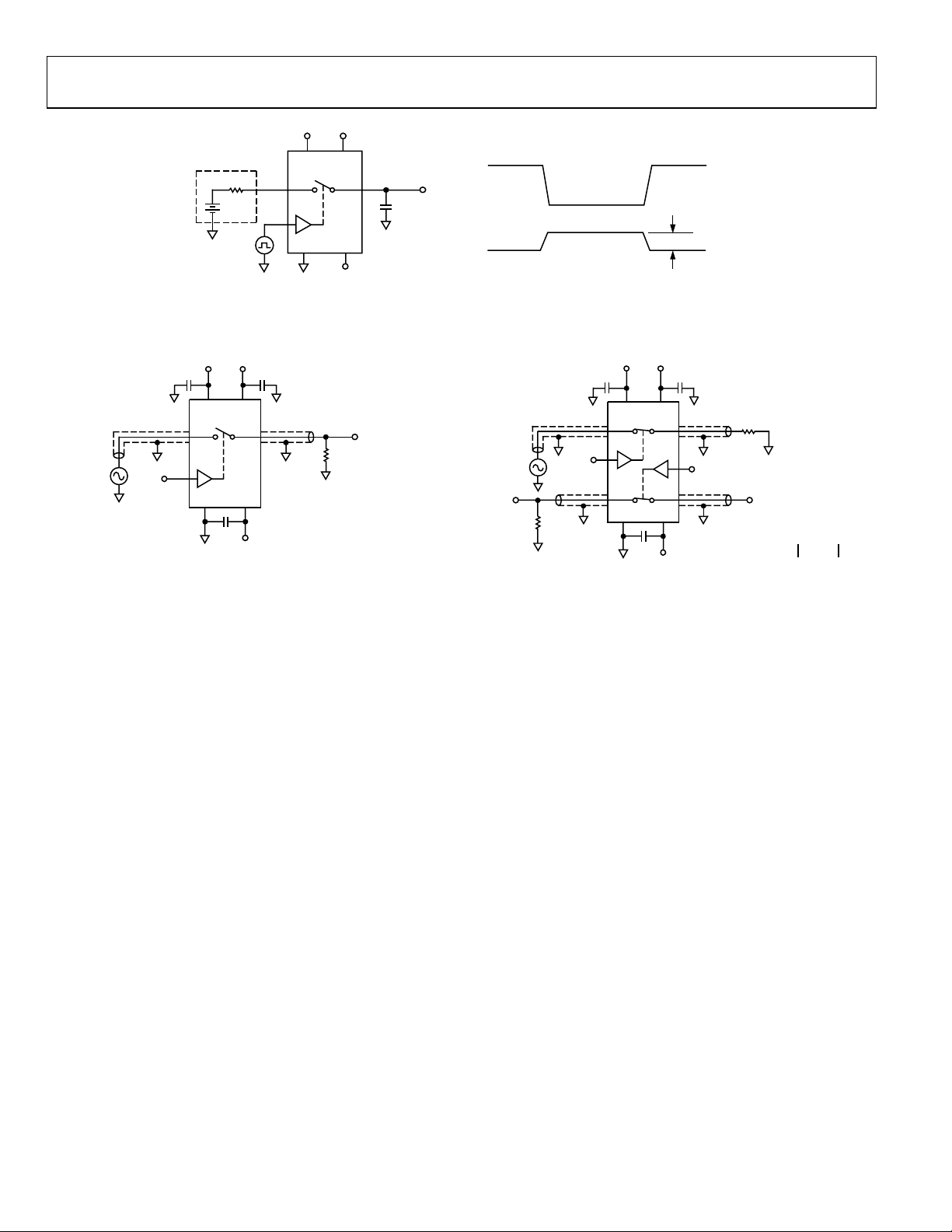
TEST CIRCUITS
I
DS
V1
SD
IS (OFF) ID (OFF)
SD
A A
SD
ID (ON)
A
V
S
RON = V1/I
DS
Figure 14. On Resistance
00024-014
V
S
V
D
00024-015
Figure 15. Off Leakage
V
S
Figure 16. On Leakage
V
D
00024-016
+15V +5V
0.1µF 0.1µF
3V
V
DDVL
S
D
R
V
S
IN
V
GND
SS
0.1µF
–15V
L
300Ω
C
L
35pF
V
OUT
V
ADG411
IN
V
IN
ADG412
V
OUT
50% 50%
3V
50% 50%
90% 90%
t
ON
t
OFF
00024-017
Figure 17. Switching Times
+15V +5V
0.1µF 0.1µF
V
DDVL
V
V
S1 D1
S1
S2
S2
IN1, IN2
V
IN
GND
0.1µF
V
–15V
D2
R
C
L2
300Ω
35pF
SS
V
L2
OUT2
R
L1
300Ω
C
L1
35pF
V
OUT1
Figure 18. Break-Before-Make Time Delay
V
V
V
OUT1
OUT2
3V
IN
0V
0V
0V
50% 50%
90%
90%
t
D
t
90%
D
90%
00024-018
Rev. C | Page 11 of 16
ADG411/ADG412/ADG413
V
V
R
S
V
S
+15V +5V
V
IN
GND
DDVL
SD
V
SS
–15V
C
L
10nF
3V
V
OUT
V
IN
V
OUT
Q
INJ
= CL× ∆V
OUT
∆
V
OUT
00024-019
Figure 19. Charge Injection
+15V +5V
F 0.1µF
0.1µ
V
DDVL
SD
IN
V
S
IN
V
GND
SS
0.1µF
–15V
V
OUT
R
L
50
Ω
00024-020
OUT
V
S
R
L
50Ω
Figure 20. Off Isolation
+15V +5V
0.1µF 0.1µF
V
DDVL
S
D
V
IN1
S
D
V
GND
0.1µF
SS
CHANNEL-TO-CHANNEL
CROSSTALK = 20 × LOG V
–15V
50Ω
V
IN2
Figure 21. Channel-to-Channel Crosstalk
NC
S/VOUT
00024-021
Rev. C | Page 12 of 16
ADG411/ADG412/ADG413
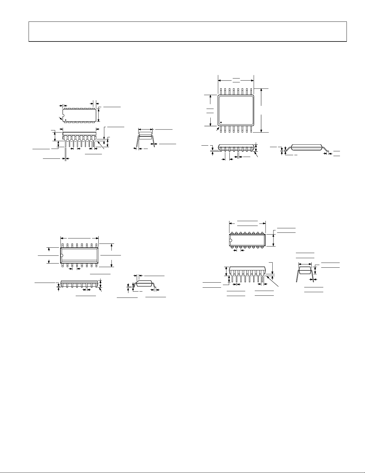
OUTLINE DIMENSIONS
0.005
(0.13)
MIN
PIN 1
0.200 (5.08)
MAX
0.200 (5.08)
0.125 (3.18)
0.023 (0.58)
0.014 (0.36)
CONTROLLING DIMENSIONS ARE IN INCHES; MILLIMETER DIMENSIONS
(IN PARENTHESES) ARE ROUNDED-OFF INCH EQUIVALENTS FOR
REFERENCE ONLY AND ARE NOT APPROPRIATE FOR USE IN DESIGN
0.098 (2.49)
MAX
16
1
0.840 (21.34) MAX
0.100
0.070 (1.78)
(2.54)
0.030 (0.76)
BSC
9
8
0.310 (7.87)
0.220 (5.59)
0.060 (1.52)
0.015 (0.38)
0.150 (3.81)
MIN
SEATING
PLANE
15°
0°
Figure 22. 16-Lead Ceramic Dual In-Line Package [CERDIP]
(Q-16)
Dimensions shown in inches and (millimeters)
10.00 (0.3937)
9.80 (0.3858)
4.00 (0.1575)
3.80 (0.1496)
0.25 (0.0098)
0.10 (0.0039)
COPLANARITY
CONTROLLING DIMENSIONS ARE IN MILLIMETERS; INCH DIMENSIONS
(IN PARENTHESES) ARE ROUNDED-OFF MILLIMETER EQUIVALENTS FOR
REFERENCE ONLY AND ARE NOT APPROPRIATE FOR USE IN DESIGN
16
1
1.27 (0.0500)
BSC
0.51 (0.0201)
0.10
0.31 (0.0122)
COMPLIANT TO JEDEC STANDARDS MS-012AC
9
6.20 (0.2441)
5.80 (0.2283)
8
1.75 (0.0689)
1.35 (0.0531)
SEATING
PLANE
0.25 (0.0098)
0.17 (0.0067)
0.50 (0.0197)
0.25 (0.0098)
8°
0°
1.27 (0.0500)
0.40 (0.0157)
Figure 23. 16-Lead Standard Small Outline Package [SOIC]
Narrow Body
(R-16)
Dimensions shown in millimeters and (inches)
0.320 (8.13)
0.290 (7.37)
0.015 (0.38)
0.008 (0.20)
× 45°
4.50
4.40
4.30
PIN 1
0.15
0.05
0.65
BSC
Figure 24. 16-Lead Thin Shrink Small Outline Package [TSSOP]
0.180 (4.57)
0.150 (3.81)
0.130 (3.30)
0.110 (2.79)
CONTROLLING DIMENSIONS ARE IN INCHES; MILLIMETER DIMENSIONS
(IN PARENTHESES) ARE ROUNDED-OFF INCH EQUIVALENTS FOR
REFERENCE ONLY AND ARE NOT APPROPRIATE FOR USE IN DESIGN
5.10
5.00
4.90
16
COPLANARITY
COMPLIANT TO JEDEC STANDARDS MO-153AB
0.10
0.30
0.19
9
81
1.20
MAX
SEATING
PLANE
6.40
BSC
0.20
0.09
8°
0°
(RU-16)
Dimensions shown in millimeters
0.785 (19.94)
0.765 (19.43)
0.745 (18.92)
16
1
0.100 (2.54)
BSC
0.015 (0.38)
MAX
0.022 (0.56)
0.018 (0.46)
0.014 (0.36)
COMPLIANT TO JEDEC STANDARDS MO-095AC
0.060 (1.52)
0.050 (1.27)
0.045 (1.14)
9
8
MIN
0.295 (7.49)
0.285 (7.24)
0.275 (6.99)
SEATING
PLANE
0.325 (8.26)
0.310 (7.87)
0.300 (7.62)
0.015 (0.38)
0.010 (0.25)
0.008 (0.20)
Figure 25. 16-Lead Plastic Dual In-Line Package [PDIP]
(N-16)
Dimensions shown in inches and (millimeters)
0.75
0.60
0.45
0.150 (3.81)
0.135 (3.43)
0.120 (3.05)
Rev. C | Page 13 of 16

ADG411/ADG412/ADG413
ORDERING GUIDE
Model Temperature Range Package Description Package Option
ADG411BN −40°C to +85°C P-DIP N-16
ADG411BR −40°C to +85°C SOIC R-16A
ADG411BR-REEL −40°C to +85°C SOIC R-16A
ADG411BR-REEL7 −40°C to +85°C SOIC R-16A
ADG411BRZ
ADG411BRZ-REEL
ADG411BRZ-REEL7
ADG411BRU −40°C to +85°C TSSOP RU-16
ADG411BRU-REEL −40°C to +85°C TSSOP RU-16
ADG411BRU-REEL7 −40°C to +85°C TSSOP RU-16
ADG411BRUZ
ADG411BRUZ-REEL
ADG411BRUZ-REEL7
ADG411TQ −55°C to +125°C CERDIP Q-16
ADG411BCHIPS DIE
ADG412BN −40°C to +85°C P-DIP N-16
ADG412BR −40°C to +85°C SOIC R-16A
ADG412BR-REEL −40°C to +85°C SOIC R-16A
ADG412BR-REEL7 −40°C to +85°C SOIC R-16A
ADG412BRZ
ADG412BRZ-REEL
ADG412BRZ-REEL7
ADG412BRU −40°C to +85°C TSSOP RU-16
ADG412BRU-REEL −40°C to +85°C TSSOP RU-16
ADG412BRU-REEL7 −40°C to +85°C TSSOP RU-16
ADG412BRUZ
ADG412BRUZ-REEL
ADG412BRUZ-REEL7
ADG412TQ −55°C to +125°C CERDIP Q-16
ADG412TCHIPS DIE
ADG413BN −40°C to +85°C P-DIP N-16
ADG413BR −40°C to +85°C SOIC R-16A
ADG413BR-REEL −40°C to +85°C SOIC R-16A
ADG413BRZ
ADG413BRZ-REEL
ADG413BRUZ
ADG413BRUZ-500RL7
ADG413BRUZ-REEL
ADG413BRUZ-REEL7
1
Z = Pb-free part.
1
1
1
1
1
1
1
1
1
1
1
1
1
1
1
1
1
1
−40°C to +85°C SOIC R-16A
−40°C to +85°C SOIC R-16A
−40°C to +85°C SOIC R-16A
−40°C to +85°C TSSOP RU-16
−40°C to +85°C TSSOP RU-16
−40°C to +85°C TSSOP RU-16
−40°C to +85°C SOIC R-16A
−40°C to +85°C SOIC R-16A
−40°C to +85°C SOIC R-16A
−40°C to +85°C TSSOP RU-16
−40°C to +85°C TSSOP RU-16
−40°C to +85°C TSSOP RU-16
−40°C to +85°C SOIC R-16A
−40°C to +85°C SOIC R-16A
−40°C to +85°C TSSOP RU-16
−40°C to +85°C TSSOP RU-16
−40°C to +85°C TSSOP RU-16
−40°C to +85°C TSSOP RU-16
Rev. C | Page 14 of 16

ADG411/ADG412/ADG413
NOTES
Rev. C | Page 15 of 16

ADG411/ADG412/ADG413
NOTES
© 2004 Analog Devices, Inc. All rights reserved. Trademarks and
registered trademarks are the property of their respective owners.
C00024–0–11/04(C)
Rev. C | Page 16 of 16
 Loading...