

LC2MOS 4-/8-Channel
www.BDTIC.com/ADI
High Performance Analog Multiplexers
FEATURES
44 V supply maximum ratings
to VDD analog signal range
V
SS
Low on resistance (100 Ω maximum)
Low power (I
Fast switching
Break-before-make switching action
Plug-in replacement for DG408/DG409
APPLICATIONS
Audio and video routing
Automatic test equipment
Data acquisition systems
Battery-powered systems
Sample-and-hold systems
Communication systems
GENERAL DESCRIPTION
The ADG408/ADG409 are monolithic CMOS analog multiplexers
comprising eight single channels and four differential channels,
respectively. The ADG408 switches one of eight inputs to a
common output as determined by the 3-bit binary address lines
A0, A1, and A2. The ADG409 switches one of four differential
inputs to a common differential output, as determined by the
2-bit binary address lines A0 and A1. An EN input on both devices
is used to enable or disable the device. When the device is disabled,
all channels are switched off.
The ADG408/ADG409 are designed on an enhanced LC
process that provides low power dissipation yet gives high
switching speed and low on resistance. Each channel conducts
equally well in both directions when on and has an input signal
range that extends to the supplies. In the off condition, signal
levels up to the supplies are blocked. All channels exhibit breakbefore-make switching action, preventing momentary shorting
when switching channels. Inherent in the design is low
charge injection for minimum transients when switching the
digital inputs.
SUPPLY
< 75 μA)
2
MOS
ADG408/ADG409
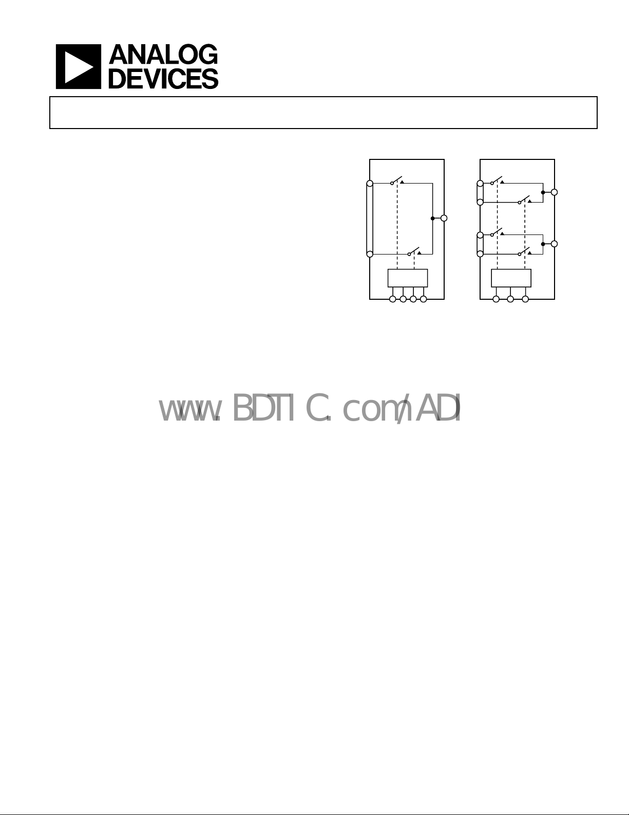
FUNCTIONAL BLOCK DIAGRAMS
ADG408
S1
S8
1-OF-8
DECODER
S1A
S4A
D
S1B
S4B
Figure 1.
PRODUCT HIGHLIGHTS
1. Extended Signal Range. The ADG408/ADG409 are
fabricated on an enhanced LC
increased signal range that extends to the supply rails.
w Power Dissipation.
2. Lo
3. Lo
4. S
analog signal is unipolar, the ADG408/ADG409 can be
operated from a single rail power supply. The parts are
fully specified with a single 12 V power supply and remain
functional with single supplies as low as 5 V.
.
w R
ON
ingle-Supply Operation. For applications where the
ADG409
1-OF-4
DECODER
A0 A1 E NA0 A1 A2 EN
2
MOS process, giving an
DA
DB
00027-001
The ADG408/ADG409 are improved replacements for the
D
G408/DG409 analog multiplexers.
Rev. C
Information furnished by Analog Devices is believed to be accurate and reliable. However, no
responsibility is assumed by Anal og Devices for its use, nor for any infringements of patents or ot her
rights of third parties that may result from its use. Specifications subject to change without notice. No
license is granted by implication or otherwise under any patent or patent rights of Analog Devices.
Trademarks and registered trademarks are the property of their respective owners.
One Technology Way, P.O. Box 9106, Norwood, MA 02062-9106, U.S.A.
Tel: 781.329.4700 www.analog.com
Fax: 781.461.3113 ©2006 Analog Devices, Inc. All rights reserved.

ADG408/ADG409
www.BDTIC.com/ADI
TABLE OF CONTENTS
Features.............................................................................................. 1
Absolute Maximum Ratings ............................................................6
Applications....................................................................................... 1
Functional Block Diagrams............................................................. 1
General Description ......................................................................... 1
Product Highlights ........................................................................... 1
Revision History ............................................................................... 2
Specifications..................................................................................... 3
Dual Supply................................................................................... 3
Single Supply................................................................................. 4
REVISION HISTORY
10/06—Rev. B to Rev. C
Updated Format..................................................................Universal
Changes to Table 3............................................................................ 6
Inserted Table 4 and Table 5............................................................ 7
Updated Outline Dimensions....................................................... 14
Changes to Ordering Guide.......................................................... 15
ESD Caution...................................................................................6
Pin Configurations and Function Descriptions............................7
Typical Performance Characteristics..............................................8
Test Circuits..................................................................................... 11
Terminology.................................................................................... 13
Outline Dimensions....................................................................... 14
Ordering Guide .......................................................................... 16
3/03—Rev. A to Rev. B
C
hanges to Ordering Guide.............................................................4
Updated Outline Dimensions....................................................... 11
2/01—Revision 0: Initial Version
Rev. C | Page 2 of 16
ADG408/ADG409
www.BDTIC.com/ADI
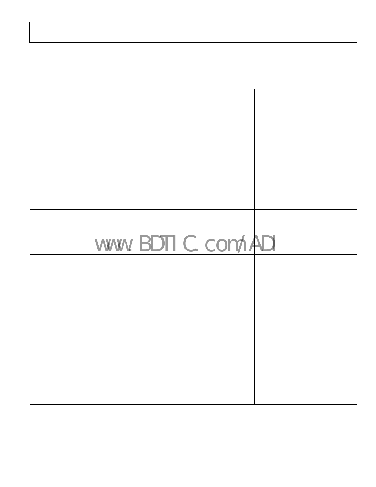
SPECIFICATIONS
DUAL SUPPLY
VDD = 15 V, VSS = −15 V, GND = 0 V, unless otherwise noted.
Table 1.
B Version T Version
−40ºC to
Parameter +25ºC
ANALOG SWITCH
Analog Signal Range VSS to VDD VSS to VDD V
RON 40 40 Ω typ
100 125 100 125 Ω max
∆RON 15 15 Ω max
LEAKAGE CURRENTS
Source Off Leakage IS (OFF) ±0.5 ±50 ±0.5 ±50 nA max VD = ±10 V, VS = 10 V; see mFigure 19
Drain Off Leakage ID (OFF) VD = ±10 V; VS = 10 V; see m Figure 20
ADG408 ±1 ±100 ±1 ±100 nA max
ADG409 ±1 ±50 ±1 ±50 nA max
Channel On Leakage ID, IS (ON) VS = VD = ±10 V; see Figure 21
ADG408 ±1 ±100 ±1 ±100 nA max
ADG409 ±1 ±50 ±1 ±50 nA max
DIGITAL INPUTS
Input High Voltage, V
Input Low Voltage, V
Input Current
I
or I
±10 ±10 μA max VIN = 0 or VDD
INL
INH
CIN, Digital Input Capacitance 8 8 pF typ f = 1 MHz
DYNAMIC CHARACTERISTICS
t
250 250 ns max VS1 = ±10 V, VS8 = 10 V; see m Figure 22
t
V
tON (EN) 85 125 85 125 ns typ RL = 300 Ω CL = 35 pF;
150 225 150 225 ns max VS = 5 V; see Figure 24
t
150 150 ns max VS = 5 V; see Figure 24
Charge Injection 20 20 pC typ VS = 0 V, RS = 0 Ω, CL = 10 nF; see Figure 25
OFF Isolation
V
Channel-to-Channel Crosstalk 85 85 dB typ RL = 1 kΩ, f = 100 kHz; see Figure 27
CS (OFF) 11 11 pF typ f = 1 MHz
CD (OFF) f = 1 MHz
CD, CS (ON) f = 1 MHz
120 120 ns typ RL = 300 Ω, CL = 35 pF;
TRANSITION
10 10 10 10 ns min RL = 300 Ω, CL = 35 pF;
OPEN
(EN) 65 65 ns typ RL = 300 Ω, CL = 35 pF;
OFF
ADG408 40 40 pF typ
ADG409 20 20 pF typ
ADG408 54 54 pF typ
ADG409 34 34 pF typ
2.4 2.4 V min
INH
0.8 0.8 V max
INL
1
−75
+85ºC +25ºC
−75
−55ºC to
+125ºC Unit Test Conditions/Comments
V
= ±10 V, IS = −10 mA
D
V
= +10 V, −10 V
D
= 5 V; see Figure 23
S
dB typ RL = 1 kΩ, f = 100 kHz;
= 0 V; see Figure 26
EN
Rev. C | Page 3 of 16
ADG408/ADG409
www.BDTIC.com/ADI
B Version T Version
−40ºC to
Parameter +25ºC
+85ºC
+25ºC
POWER REQUIREMENTS
IDD 1 1 μA typ VIN = 0 V, VEN = 0 V
5 5 μA max
ISS 1 1 μA typ
5 5 μA max
IDD 100 100 μA typ VIN = 0 V, VEN = 2.4 V
200 500 200 500 μA max
1
Guaranteed by design, not subject to production test.
SINGLE SUPPLY
VDD = 12 V, VSS = 0 V, GND = 0 V, unless otherwise noted.
Table 2.
B Version T Version
−40ºC to
Parameter +25ºC
ANALOG SWITCH
Analog Signal Range 0 to VDD 0 to VDD V
RON 90 90 Ω typ VD = 3 V, 10 V, IS = –1 mA
LEAKAGE CURRENTS
Source Off Leakage IS (OFF) ±0.5 ±50 ±0.5 ±50 nA max VD = 8 V/0 V, VS = 0 V/8 V; see Figure 19
Drain Off Leakage ID (OFF) VD = 8 V/0 V, VS = 0 V/8 V; see Figure 20
ADG408 ±1 ±100 ±1 ±100 nA max
ADG409 ±1 ±50 ±1 ±50 nA max
Channel On Leakage ID, IS (ON) VS = VD = 8 V/0 V; see Figure 21
ADG408 ±1 ±100 ±1 ±100 nA max
ADG409 ±1 ±50 ±1 ±50 nA max
DIGITAL INPUTS
Input High Voltage, V
Input Low Voltage, V
2.4 2.4 V min
INH
0.8 0.8 V max
INL
Input Current
I
or I
±10 ±10 μA max VIN = 0 or VDD
INL
INH
C
Digital Input Capacitance 8 8 pF typ f = 1 MHz
IN,
DYNAMIC CHARACTERISTICS
t
130 130 ns typ RL = 300 Ω, CL = 35 pF;
TRANSITION
1
V
t
OPEN
10 10 ns typ
V
tON (EN) 140 140 ns typ RL = 300 Ω CL = 35 pF;
V
t
(EN) 60 60 ns typ RL = 300 Ω, CL = 35 pF;
OFF
V
Charge Injection 5 5 pC typ VS = 0 V, RS = 0Ω, CL = 10 nF; see Figure 25
Off Isolation –75 –75 dB typ RL = 1 kΩ f = 100 kHz;
V
+85ºC +25°C
−55ºC to
+125ºC
Unit Test Conditions/Comments
−55ºC to
+125ºC Unit Test Conditions/Comments
= 8 V/0 V, VS8 = 0 V/8 V; see Figure 22
S1
RL = 300 Ω, CL = 35 pF;
= 5 V; see Figure 23
S
= 5 V; see Figure 24
S
= 5 V; see Figure 24
S
= 0 V; see Figure 26
EN
Rev. C | Page 4 of 16
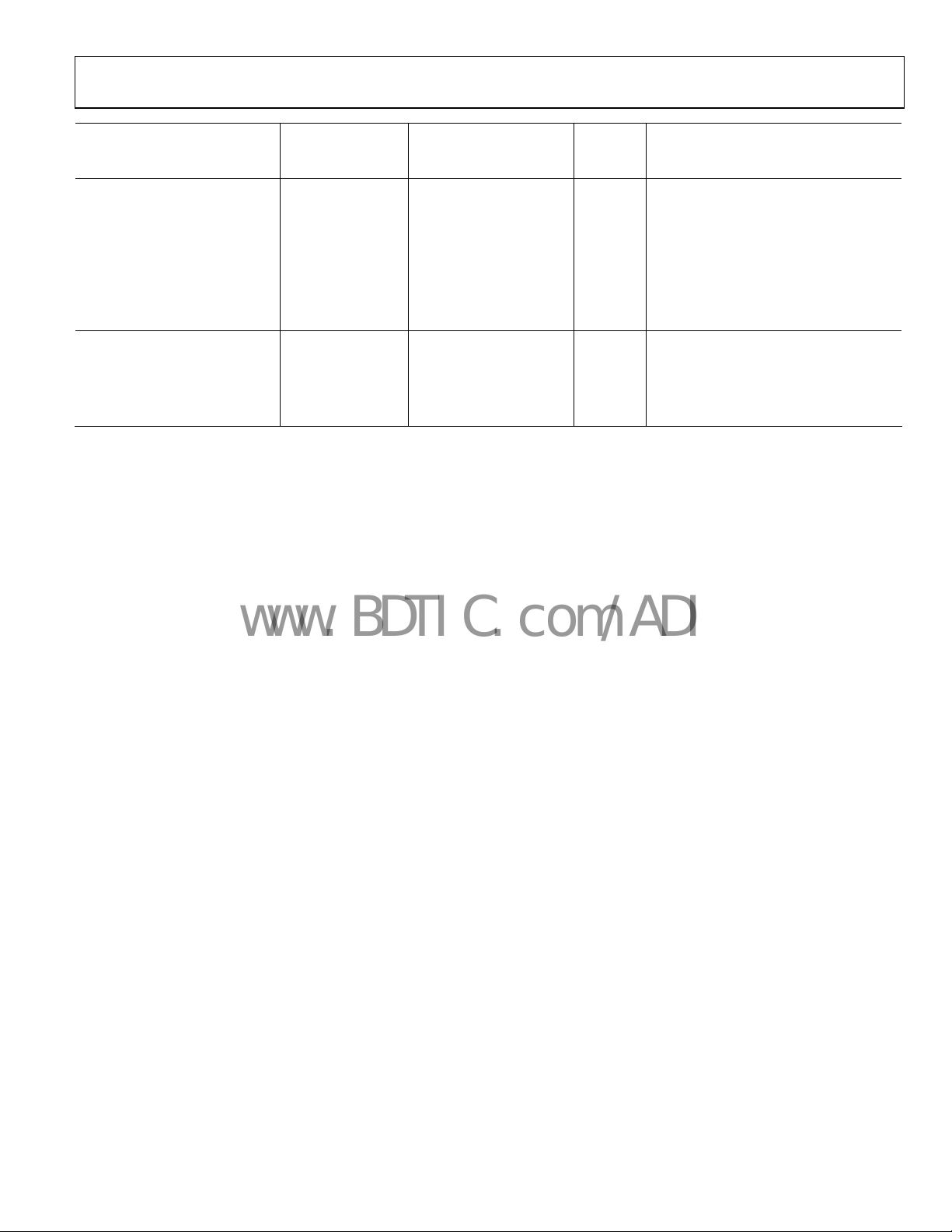
ADG408/ADG409
www.BDTIC.com/ADI
B Version T Version
−40ºC to
Parameter +25ºC
Channel-to-Channel Crosstalk 85 85 dB typ RL = 1 kΩ, f = 100 kHz; see Figure 27
CS (OFF) 11 11 pF typ f = 1 MHz
CD (OFF) f = 1 MHz
ADG408 40 40 pF typ
ADG409 20 20 pF typ
CD, CS (ON) f = 1 MHz
ADG408 54 54 pF typ
ADG409 34 34 pF typ
POWER REQUIREMENTS
IDD 1 1 μA typ VIN = 0 V, VEN = 0 V
5 5 μA max
IDD 100 100 μA typ VIN = 0 V, VEN = 2.4 V
200 500 200 500 μA max
1
Guaranteed by design, not subject to production test.
+85ºC
+25°C
−55ºC to
+125ºC
Unit Test Conditions/Comments
Rev. C | Page 5 of 16

ADG408/ADG409
www.BDTIC.com/ADI
ABSOLUTE MAXIMUM RATINGS
TA = 25°C, unless otherwise noted.
Table 3.
Parameter Rating
VDD to VSS 44 V
VDD to GND −0.3 V to +32 V
V
to GND +0.3 V to −32 V
SS
Analog, Digital Inputs
Continuous Current, S or D 20 mA
Peak Current, S or D
(Pulsed at 1 ms, 10% Duty Cycle
Maximum)
Operating Temperature Range
Industrial (B Version) −40° C to +85°C
Extended (T Version) −55° C to +125°C
Storage Temperature Range −65° C to +150°C
Junction Temperature 150°C
CERDIP Package, Power Dissipation 900 mW
θJA, Thermal Impedance 76°C/W
Lead Temperature, Soldering
(10 sec)
PDIP Package, Power Dissipation 470 mW
θ
Thermal Impedance 117°C/W
JA,
Lead Temperature, Soldering
(10 sec)
TSSOP Package, Power Dissipation 450 mW
θJA, Thermal Impedance 155°C/W
θJC, Thermal Impedance 50°C/W
SOIC Package, Power Dissipation 600 mW
θJA, Thermal Impedance 77°C/W
Lead Temperature, Soldering
Vapor Phase (60 sec) 215°C
Infrared (15 sec) 220°C
− 2 V to VDD + 2 V or 20 mA,
V
SS
whichever occurs first
40 mA
300°C
260°C
Stresses above those listed under Absolute Maximum Ratings
ma
y cause permanent damage to the device. This is a stress
rating only; functional operation of the device at these or any
other conditions above those indicated in the operational
section of this specification is not implied. Exposure to absolute
maximum rating conditions for extended periods may affect
device reliability.
ESD CAUTION
Rev. C | Page 6 of 16

ADG408/ADG409
V
www.BDTIC.com/ADI
PIN CONFIGURATIONS AND FUNCTION DESCRIPTIONS
A0
A0
EN
SS
S1
S2
S3
S4
D
1
2
3
ADG408
4
TOP VIEW
(Not to Scale)
5
6
7
8
16
A1
A2
15
GND
14
13
V
DD
S5
12
S6
11
10
S7
S8
9
00027-002
Figure 2. ADG408 Pin Configuration
Table 4. ADG408 Pin Function Descriptions
Pin
No.
Mnemonic Description
1 A0 Logic Control Input.
2 EN
Active High Digital Input. When low, the
evice is disabled and all switches are off.
d
When high, Ax logic inputs determine on
switches.
3 VSS
Most Negative Power Supply Potential in
Supplies. In single-supply applications,
Dual
it can be connected to ground.
4 S1
Source Terminal 1. Can be an input or
an output.
5 S2
Source Terminal 2. Can be an input or
an output.
6 S3
Source Terminal 3. Can be an input or
an output.
7 S4
Source Terminal 4. Can be an input or
an output.
8 D
Drain Terminal. Can be an input or an
output.
9 S8
Source Terminal 8. Can be an input or
an output.
10 S7
Source Terminal 7. Can be an input or
an output.
11 S6
Source Terminal 6. Can be an input or
an output.
12 S5
Source Terminal 5. Can be an input or
an output.
13 VDD Most Positive Power Supply Potential.
14 GND Ground (0 V) Reference.
15 A2 Logic Control Input.
16 A1 Logic Control Input.
Table 6. ADG408 Truth Table
A2 A1 A0 EN ON SWITCH
X X X 0 NONE
0 0 0 1 1
0 0 1 1 2
0 1 0 1 3
0 1 1 1 4
1 0 0 1 5
1 0 1 1 6
1 1 0 1 7
1 1 1 1 8
1
EN
2
3
V
ADG409
SS
DA
TOP VIEW
4
(Not to Scale)
5
6
7
8
S1A
S2A
S3A
S4A
Figure 3. ADG409 Pin Configuration
Table 5. ADG409 Pin Function Descriptions
Pin
No.
Mnemonic Description
1 A0 Logic Control Input.
2 EN
Active High Digital Input. When low, the
evice is disabled and all switches are off.
d
When high, Ax logic inputs determine on
switches.
3 VSS
Most Negative Power Supply Potential in
Supplies. In single-supply applications,
Dual
it can be connected to ground.
4 S1A
Source Terminal 1A. Can be an input or
an output.
5 S2A
Source Terminal 2A. Can be an input or
an output.
6 S3A
Source Terminal 3A. Can be an input or
an output.
7 S4A
Source Terminal 4A. Can be an input or
an output.
8 DA
Drain Terminal A. Can be an input or an
output.
9 DB
Drain Terminal B. Can be an input or an
output.
10 S4B
Source Terminal 4B. Can be an input or
an output.
11 S3B
Source Terminal 3B. Can be an input or
an output.
12 S2B
Source Terminal 2B. Can be an input or
an output.
13 S1B
Source Terminal 1B. Can be an input or
an output.
14 VDD Most Positive Power Supply Potential.
15 GND Ground (0 V) Reference.
16 A1 Logic Control Input.
Table 7. ADG409 Truth Table
ON SWITCH
A1 A0 EN PAIR
X X 0 NONE
0 0 1 1
0 1 1 2
1 0 1 3
1 1 1 4
A1
16
GND
15
14
V
DD
13
S1B
S2B
12
S3B
11
S4B
10
DB
9
00027-003
Rev. C | Page 7 of 16

ADG408/ADG409
www.BDTIC.com/ADI
TYPICAL PERFORMANCE CHARACTERISTICS
120
TA=25°C
100
80
(Ω)
VDD=+10V
= –10V
V
ON
SS
R
60
40
20
–15 –10 –5 0 5 10 15
VD[VS](V)
VDD=+5V
=–5V
V
SS
VDD= +12V
V
SS
VDD= +15V
=–15V
V
SS
= –12V
Figure 4. RON as a Function of VD (VS): Dual-Supply Voltage
00027-004
180
160
140
120
(Ω)
ON
R
100
80
60
40
0369121
VDD=5V
=0V
V
SS
VDD=10V
V
SS
VD[VS](V)
=0V
TA=25°C
VDD=12V
=0V
V
SS
VDD=15V
=0V
V
SS
Figure 7. RON as a Function of VD (VS): Single-Supply Voltage
5
00027-007
100
VDD=+15V
= –15V
V
SS
90
80
70
(Ω)
ON
R
60
50
40
30
–15 –10 –5 0 5 10 15
Figure 5. R
0.2
0.1
0
LEAKAGE CURRENT (n A)
–0.1
125°C
85°C
25°C
](V)
V
D[VS
as a Function of VD (VS) for Different Temperatures
ON
TA= 25°C
V
=+15V
DD
V
= –15V
SS
IS(OFF)
ID(OFF)
I
(ON)
D
130
VDD=12V
=0V
V
SS
120
110
100
(Ω)
ON
R
90
80
70
60
024681012
00027-005
Figure 8. R
0.04
0.02
0
–0.02
LEAKAGE CURRENT (n A)
–0.04
125°C
85°C
25°C
VD[VS](V)
as a Function of VD (VS) for Different Temperature
ON
TA= 25°C
=12V
V
DD
=0V
V
SS
(ON)
I
D
(OFF)
I
D
(OFF)
I
S
00027-008
–0.2
–15 –10 –5 0 5 10 15
V
D[VS
](V)
00027-006
Figure 6. Leakage Currents as a Function of VD (VS)
Rev. C | Page 8 of 16
–0.06
024681012
Figure 9. Leakage Currents as a Function of V
VD[VS](V)
D
(VS)
0027-009

ADG408/ADG409
www.BDTIC.com/ADI
120
100
80
TIME (ns)
60
40
20
400
300
200
TIME (ns)
100
t
TRANSITION
t
(EN)
ON
t
(EN)
OFF
13579111315
Figure 10. Switching Time vs. V
t
TRANSITI ON
t
(EN)
ON
t
(EN)
OFF
(V)
V
IN
IN
VDD= +15V
V
= –15V
SS
(Bipolar Supply)
V
IN
=5V
00027-010
140
VDD=12V
=0V
V
SS
120
100
TIME (ns)
80
60
40
135791113
VIN(V)
t
TRANSITI ON
t
(EN)
ON
t
(EN)
OFF
Figure 13. Switching Time vs. VIN (Single Supply)
TIME (ns)
300
200
100
t
OFF
t
TRANSITI ON
t
(EN)
ON
(EN)
=5V
V
IN
00027-013
0
57911131
V
SUPPLY
(V)
Figure 11. Switching Time vs. Single Supply
10k
VDD= +15V
V
= –15V
SS
1k
(µA)
DD
I
EN = 2.4V
EN = 0V
100
10 100 1k 10k 100k 1M 10M
FREQUENCY (Hz)
Figure 12. Positive Supply Current vs. Switching Frequency
5
00027-011
0027-012
0
±5 ±15±7
±9 ±11 ±13
V
SUPPLY
(V)
Figure 14. Switching Time vs. Bipolar Supply
10k
VDD= +15V
=–15V
V
SS
1k
100
(µA)
SS
I
10
0
–10
10 100 1k 10k 100k 1M 10M
EN = 2.4V
EN = 0V
FREQUENCY (Hz)
Figure 15. Negative Supply Current vs. Switching Frequency
00027-014
00027-015
Rev. C | Page 9 of 16

ADG408/ADG409
www.BDTIC.com/ADI
110
100
90
OFF ISOLATION (dB)
80
VDD= +15V
= –15V
V
SS
CROSSTALK (d B)
110
100
VDD=+15V
= –15V
V
SS
90
80
70
70
1k 10k 100k 1M
FREQUENCY (Hz)
00027-016
Figure 16. Off Isolation vs. Frequency
60
1k 100k 1M
10k
FREQUENCY ( Hz)
0027-017
Figure 17. Cross talk vs. Frequency
Rev. C | Page 10 of 16

ADG408/ADG409
V
V
VSSV
VDDV
VDDV
VDDV
www.BDTIC.com/ADI
TEST CIRCUITS
I
DS
V1
SD
S
RON=V1/I
DS
00027-018
S
Figure 18. On Resistance
V
V
DD
SS
V
V
DD
GND
SS
D
0.8V
EN
00027-019
V
S
IS(OFF)
S1
A
V
S
S2
S8
V
D
Figure 19. IS (OFF)
3V
ADDRESS
DRIVE (V
0V
t
TRANSITION
OUTPUT
)
IN
50% 50%
90%
t
r
t
f
< 20ns
< 20ns
t
TRANSITION
90%
A0
V
IN
50Ω
2.4V EN
A1
A2
S1
S2
S8
S1
S8
V
DDVSS
ADG408
GND
DD
V
V
SS
DD
EN
GND
Figure 20. ID (OFF)
SS
V
V
DD
SS
EN
GND
Figure 21. ID (ON)
SS
S1
S2–S7
S8
1
OUTPUT
D
D
0.8V
D
2.4V
V
V
300Ω
ID(OFF)
A
V
D
00027-020
ID(ON)
A
V
D
00027-021
S1
S8
35pF
Figure 22. Switching Time of Multiplexer, t
3V
ADDRESS
DRIVE (V
)
IN
0V
OUTPUT
80% 80%
t
OPEN
Figure 23. Break-Before-Make Delay, t
Rev. C | Page 11 of 16
1
SIMILAR CONNECTION F OR ADG409.
TRANSlTlON
SS
V
DDVSS
A0
V
IN
50Ω
A1
A2
ADG408
2.4V EN
1
SIMILAR CONNECTION F OR ADG409.
OPEN
GND
S2–S7
1
S1
S8
D
V
OUTPUT
300Ω
S
35pF
00027-022
00027-023

ADG408/ADG409
VDDV
O
R
VINV
VDDV
VSVSSV
VSSV
www.BDTIC.com/ADI
SS
3V
ENABLE
D
IVE (VIN)
0V
UTPUT
50% 50%
t
0.9V
OFF
(EN)
O
V
IN
50Ω
1
SIMILAR CONNECTION F OR ADG409.
(EN), t
OFF
(EN)
ON
t
(EN)
ON
0.9V
O
Figure 24. Enable Delay, t
V
A0
A1
A2
EN
DDVSS
ADG408
GND
S2–S8
1
S1
D
OUTPUT
300Ω
V
S
35pF
00027-024
SS
V
DDVSS
A0
A1
A2
GND
1
DS
C
L
10nF
V
OUT
ADG408
EN
V
IN
OUT
3V
R
S
V
S
Q
INJ=CL
× ΔV
OUT
ΔV
OUT
1
SIMILAR CONNECTI ON FOR ADG409.
00027-025
Figure 25. Charge Injection
DD
V
V
A0
A1
A2
S1
S8
0V
EN
OFF ISOLATION = 20 log V
DD
ADG408
GND
SS
Figure 26. Off Isolation
D
OUT/VIN
1kΩ
V
OUT
V
S
00027-026
Figure 27. Channel-to-Channel Crosstalk
DD
V
V
A0
A1
A2
S1
S2
S8
CROSSTALK = 20 log V
DD
ADG408
GND
SS
EN
D
OUT/VIN
2.4V
V
OUT
1kΩ1kΩ
0027-027
Rev. C | Page 12 of 16

ADG408/ADG409
www.BDTIC.com/ADI
TERMINOLOGY
RON
Ohmic resistance between D and S.
ΔR
ON
Difference between the RON of any two channels.
(OFF)
I
S
Source leakage current when the switch is off.
I
(OFF)
D
Drain leakage current when the switch is off.
I
, IS (ON)
D
Channel leakage current when the switch is on.
(VS)
V
D
Analog voltage on Terminal D and Terminal S.
C
(OFF)
S
Channel input capacitance for off condition.
C
(OFF)
D
Channel output capacitance for off condition.
, CS (ON)
C
D
On switch capacitance.
C
IN
Digital input capacitance.
(EN)
t
ON
Delay time between the 50% and 90% points of the digital input
and switch on condition.
(EN)
t
OFF
Delay time between the 50% and 90% points of the digital input
and switch off condition.
t
TRANSITION
Delay time between the 50% and 90% points of the digital
inputs and the switch on condition when switching from one
address state to another.
t
OPEN
Off time measured between the 80% point of both switches
when switching from one address state to another.
V
INL
Maximum input voltage for Logic 0.
V
INH
Minimum input voltage for Logic 1.
(I
INL
INH
)
I
Input current of the digital input.
Crosstalk
A
measure of unwanted signal that is coupled through from one
channel to another as a result of parasitic capacitance.
Off Isolation
ure of unwanted signal coupling through an off channel.
A meas
Charge Injection
A m
easure of the glitch impulse transferred from the digital
input to the analog output during switching.
I
DD
Positive supply current.
I
SS
Negative supply current.
Rev. C | Page 13 of 16

ADG408/ADG409
0
www.BDTIC.com/ADI
OUTLINE DIMENSIONS
0.800 (20.32)
0.790 (20.07)
0.780 (19.81)
0.210
(5.33)
0.150 (3.81)
0.130 (3.30)
0.115 (2.92)
0.022 (0.56)
0.018 (0.46)
0.014 (0.36)
16
1
PIN 1
0.100 (2.54)
BSC
MAX
0.070 (1.78)
0.060 (1.52)
0.045 (1.14)
CONTROLLING DIMENSIONS ARE IN INCHES; MILLIMETER DIMENSIONS
(IN PARENTHESES) ARE ROUNDED-OFF INCH EQUIVALENTS FOR
REFERENCE ONLY AND ARE NOT APPROPRIATE FOR USE IN DESIGN.
CORNER LEADS MAY BE CONFIGURED AS WHOLE OR HALF LEADS.
COMPLIANT TO JEDEC STANDARDS MS-001-AB
Figure 28. 16-Lead Plastic Dual In-Line Package [PDIP]
Dimensions shown in inches and (millimeters)
9
8
0.280 (7.11)
0.250 (6.35)
0.240 (6.10)
0.015
(0.38)
MIN
SEATING
PLANE
0.005 (0.13)
MIN
Nar
row Body
(N-16)
0.060 (1.52)
MAX
0.015 (0.38)
GAUGE
PLANE
0.325 (8.26)
0.310 (7.87)
0.300 (7.62)
0.430 (10.92)
MAX
0.195 (4.95)
0.130 (3.30)
0.115 (2.92)
0.014 (0.36)
0.010 (0.25)
0.008 (0.20)
0.005 (0.13) MIN
16
1
PIN 1
0.100 (2.54) BSC
0.840 (21.34) MAX
.200 (5.08)
MAX
0.200 (5.08)
0.125 (3.18)
0.023 (0.58)
0.014 (0.36)
CONTROLLING DIMENSIONS ARE IN INCHES; MILLIMETER DIMENSIONS
(IN PARENTHESES) ARE ROUNDED-OFF INCH EQUIVALENTS FOR
REFERENCE ONLY AND ARE NOT APPROPRIATE FOR USE IN DESIGN.
Figure 29. 16-Lead Ceramic Dual In-Line Package [CERDIP]
Dim
0.098 (2.49) MAX
9
0.310 (7.87)
0.220 (5.59)
8
0.060 (1.52)
0.015 (0.38)
0.150
(3.81)
MIN
0.070 (1.78)
0.030 (0.76)
SEATING
PLANE
15°
0°
(Q-16)
ensions shown in inches and (millimeters)
0.320 (8.13)
0.290 (7.37)
0.015 (0.38)
0.008 (0.20)
Rev. C | Page 14 of 16

ADG408/ADG409
www.BDTIC.com/ADI
4.00 (0.1575)
3.80 (0.1496)
0.25 (0.0098)
0.10 (0.0039)
COPLANARITY
CONTROLLING DIMENSIONS ARE IN MILLIMETERS; INCH DIMENSIONS
(IN PARENTHESES) ARE ROUNDED-OFF MILLIMETER EQUIVALENTS FOR
REFERENCE ONLY AND ARE NOT APPROPRIATE FOR USE IN DESIGN.
10.00 (0.3937)
9.80 (0.3858)
16
1
1.27 (0.0500)
BSC
0.51 (0.0201)
0.10
0.31 (0.0122)
COMPLIANT TO JEDEC STANDARDS MS-012-AC
9
6.20 (0.2441)
5.80 (0.2283)
8
1.75 (0.0689)
1.35 (0.0531)
SEATING
PLANE
0.25 (0.0098)
0.17 (0.0067)
0.50 (0.0197)
0.25 (0.0098)
8°
0°
1.27 (0.0500)
0.40 (0.0157)
× 45°
Figure 30. 16-Lead Standard Small Outline Package [SOIC_N]
Na
rrow Body
(R-16)
Dimensions shown in millimeters and (inches)
5.10
5.00
4.90
0.15
0.05
16
4.50
4.40
4.30
PIN 1
0.65
BSC
COPLANARITY
0.10
COMPLIANT TO JEDEC STANDARDS MO-153-AB
Figure 31. 16-Lead Thin Shrink S
9
6.40
BSC
81
1.20
MAX
0.30
0.19
SEATING
PLANE
0.20
0.09
mall Outline Package [TSSOP]
(RU-16)
Dimensions shown in millimeters
8°
0°
0.75
0.60
0.45
Rev. C | Page 15 of 16

ADG408/ADG409
www.BDTIC.com/ADI
ORDERING GUIDE
Model Temperature Range Package Description Package Option
ADG408BN
ADG408BNZ
1
ADG408BR
ADG408BR-REEL
ADG408BR-REEL7
ADG408BRU
ADG408BRU-REEL
ADG408BRU-REEL7
ADG408BRUZ
1
ADG408BRUZ-REEL
ADG408BRUZ-REEL7
ADG408BRZ
ADG408BRZ-REEL
1
1
ADG408BRZ-REEL7
ADG408TQ
ADG408BCHIPS
ADG409BN
ADG409BNZ
1
ADG409BR
ADG409BR-REEL
ADG409BR-REEL7
ADG409BRU
ADG409BRU-REEL
ADG409BRU-REEL7
ADG409BRUZ
1
ADG409BRUZ-REEL
ADG409BRUZ-REEL7
ADG409BRZ
ADG409BRZ-REEL
1
1
ADG409BRZ-REEL7
ADG409TQ
1
Z = Pb-free part.
−40°C to +85°C
−40°C to +85°C
−40°C to +85°C
−40°C to +85°C
−40°C to +85°C
−40°C to +85°C
−40°C to +85°C
−40°C to +85°C
−40°C to +85°C
1
1
−40°C to +85°C
−40°C to +85°C
−40°C to +85°C
−40°C to +85°C
1
−40°C to +85°C
−55°C to +125°C
−40°C to +85°C
−40°C to +85°C
−40°C to +85°C
−40°C to +85°C
−40°C to +85°C
−40°C to +85°C
−40°C to +85°C
−40°C to +85°C
−40°C to +85°C
1
1
−40°C to +85°C
−40°C to +85°C
−40°C to +85°C
−40°C to +85°C
1
−40°C to +85°C
−55°C to +125°C
16-Lead Plastic Dual In-Line Package [PDIP]
16-Lead Plastic Dual In-Line Package [PDIP]
16-Lead Narrow Body Small Outline Package [SOIC_N]
16-Lead Narrow Body Small Outline Package [SOIC_N]
16-Lead Narrow Body Small Outline Package [SOIC_N]
16-Lead Thin Shrink Small Outline Package [TSSOP]
16-Lead Thin Shrink Small Outline Package [TSSOP]
16-Lead Thin Shrink Small Outline Package [TSSOP]
16-Lead Thin Shrink Small Outline Package [TSSOP]
16-Lead Thin Shrink Small Outline Package [TSSOP]
16-Lead Thin Shrink Small Outline Package [TSSOP]
16-Lead Narrow Body Small Outline Package [SOIC_N]
16-Lead Narrow Body Small Outline Package [SOIC_N]
16-Lead Narrow Body Small Outline Package [SOIC_N]
16-Lead Ceramic Dual In-Line Package [CERDIP]
DIE
16-Lead Plastic Dual In-Line Package [PDIP]
16-Lead Plastic Dual In-Line Package [PDIP]
16-Lead Narrow Body Small Outline Package [SOIC_N]
16-Lead Narrow Body Small Outline Package [SOIC_N]
16-Lead Narrow Body Small Outline Package [SOIC_N]
16-Lead Thin Shrink Small Outline Package [TSSOP]
16-Lead Thin Shrink Small Outline Package [TSSOP]
16-Lead Thin Shrink Small Outline Package [TSSOP]
16-Lead Thin Shrink Small Outline Package [TSSOP]
16-Lead Thin Shrink Small Outline Package [TSSOP]
16-Lead Thin Shrink Small Outline Package [TSSOP]
16-Lead Narrow Body Small Outline Package [SOIC_N]
16-Lead Narrow Body Small Outline Package [SOIC_N]
16-Lead Narrow Body Small Outline Package [SOIC_N]
16-Lead Ceramic Dual In-Line Package [CERDIP]
N-16
N-16
R-16
R-16
R-16
RU-16
RU-16
RU-16
RU-16
RU-16
RU-16
R-16
R-16
R-16
Q-16
N-16
N-16
R-16
R-16
R-16
RU-16
RU-16
RU-16
RU-16
RU-16
RU-16
R-16
R-16
R-16
Q-16
©2006 Analog Devices, Inc. All rights reserved. Trademarks and
registered trademarks are the property of their respective owners.
C00027-0-10/06(C)
Rev. C | Page 16 of 16
 Loading...