


A
1.65 V to 3.6 V, Single-Channel Level
FEATURES
Operates from 1.65 V to 3.6 V supply rails
Unidirectional signal path
Up/down level translation
Ultracompact 6-lead SOT-66 and SOT-23 packages
Output short-circuit protection
LVTTL/CMOS-compatible inputs
APPLICATIONS
Level translation in:
PDAs
Handsets
MP3 players
GENERAL DESCRIPTION
The ADG32311 is a single-channel level translator designed on a
submicron process that is guaranteed to operate over the 1.65 V
to 3.6 V supply range. The device may be used in applications
requiring communication between digital devices operating
from multiple supply voltages. The logic levels on each side of
the device are set by the two supply voltages, V
for Y. The signal path is unidirectional, meaning data may
V
CC2
flow only from A to Y.
for A and
CC1
Translator in SOT-66 Package
ADG3231
FUNCTIONAL BLOCK DIAGRAM
V
CC1
PRODUCT HIGHLIGHTS
1. Up/down level translation.
2. Guaranteed to operate with any supply combination within
the 1.65 V to 3.6 V range.
3. Output short-circuit protection.
4. Available in ultracompact SOT-66 and SOT-23 packages.
GND
Figure 1.
V
CC2
Y
03298-001
The ADG3231 can operate with any combination of V
and V
allowing the part to perform either up (V
(V
supply voltages within the 1.65 V to 3.6 V range,
CC2
CC1
> V
CC1
) level translation. The output stage is protected
CC2
< V
CC2
CC1
) or down
against current overload, which may occur when the Y pin is
accidentally shorted to the V
or GND rails.
CC2
The ADG3231 is available in ultracompact packages, the
SOT-66 (1.65 mm × 1.66 mm × 0.57 mm) and the SOT-23
(2.8 mm × 2.9 mm × 1.3 mm), making the part ideal for
applications where space is critical.
1
Patent pending.
Rev. A
Information furnished by Analog Devices is believed to be accurate and reliable.
However, no responsibility is assumed by Analog Devices for its use, nor for any
infringements of patents or other rights of third parties that may result from its use.
Specifications subject to change without notice. No license is granted by implication
or otherwise under any patent or patent rights of Analog Devices. Trademarks and
registered trademarks are the property of their respective owners.
One Technology Way, P.O. Box 9106, Norwood, MA 02062-9106, U.S.A.
Tel: 781.329.4700
Fax: 781.326.8703 © 2004 Analog Devices, Inc. All rights reserved.
www.analog.com

ADG3231
TABLE OF CONTENTS
Specifications..................................................................................... 3
Typical Performance Characteristics..............................................6
Absolute Maximum Ratings............................................................ 4
ESD Caution.................................................................................. 4
Pin Configurations and Function Descriptions ........................... 5
REVISION HISTORY
12/04—Rev. 0 to Rev. A
Updated Format..................................................................Universal
Added SOT-66 Package .....................................................Universal
Change to Data Sheet Title.............................................................. 1
Changes to Features, Applications, General Description
and Product Highlights Sections.................................................... 1
Added Patent Information .............................................................. 1
Changes to Figure 1.......................................................................... 1
Changes to Table 1............................................................................ 3
Changes to Figure 2 and Figure 3................................................... 3
Deleted TPC 1 to TPC 6 .................................................................. 6
Changes to Figure 13 through Figure 20....................................... 7
Changes to Theory of Operation Section...................................... 9
Updated Outline Dimensions....................................................... 10
Changes to Ordering Guide.......................................................... 10
Theory of Operation .........................................................................9
Outline Dimensions....................................................................... 10
Ordering Guide .......................................................................... 10
5/03—Revision 0: Initial Version
Rev. A | Page 2 of 12
ADG3231
SPECIFICATIONS
V
= V
CC1
= 1.65 V to 3.6 V, GND = 0 V. All specifications T
CC2
−40°C to +85°C.
Table 1.
Parameter Symbol Conditions Min Typ1 Max Unit
LOGIC INPUTS/OUTPUTS
Input High Voltage2 V
V
V
V
IH
V
IH
V
IH
Input Low Voltage2 V
V
V
V
IL
V
IL
V
IL
Output High Voltage VOH I
V
V
I
V
I
Output Low Voltage VOL I
V
V
I
V
I
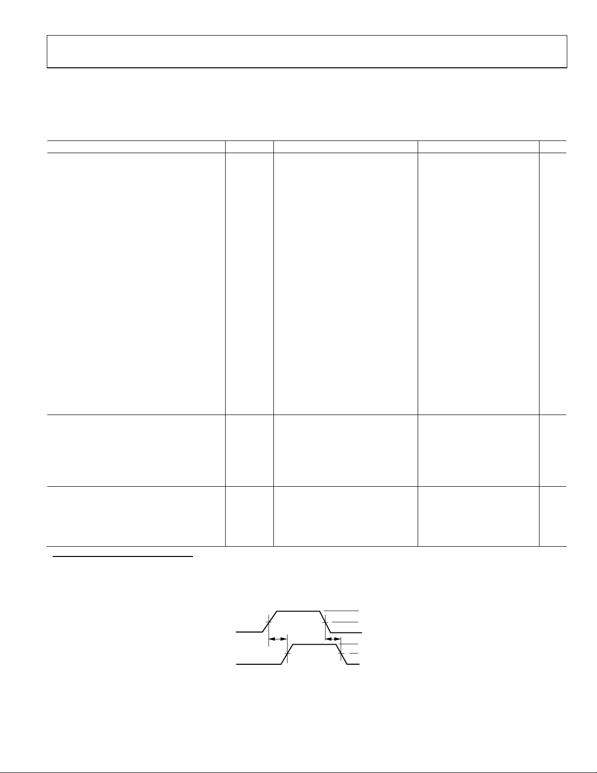
SWITCHING CHARACTERISTICS2
Propagation Delay, tPD A to Y t
Propagation Delay, tPD A to Y t
Propagation Delay, tPD A to Y t
, t
3.3 V ± 0.3 V, CL = 30 pF, Figure 2 4 6.5 ns
PHL
PLH
, t
2.5 V ± 0.2 V, CL = 30 pF, Figure 2 4.5 6.5 ns
PHL
PLH
, t
1.8 V ± 0.15 V, CL = 30 pF, Figure 2 6.5 10.25 ns
PHL
PLH
Input Leakage Current II 0 ≤ VIN ≤ 3.6 V ±1 µA
Output Leakage Current IO 0 ≤ VIN ≤ 3.6 V ±1 µA
POWER REQUIREMENTS
Power Supply Voltages V
V
Quiescent Power Supply Current I
I
1.65 3.6 V
CC1
1.65 3.6 V
CC2
Digital inputs = 0 V or V
CC1
Digital inputs = 0 V or V
CC2
1
All typical values are at V
2
Guaranteed by design, not subject to production test.
= V
, TA = 25°C, unless otherwise stated.
CC1
CC2
INPUT
t
PLH
OUTPUT
to T
MIN
CC1
CC1
CC1
CC1
CC1
CC1
= –100 µA, V
OH
= −4 mA, V
OH
= −8 mA, V
OH
= 100 µA, V
OH
= 4 mA, V
OH
= 8 mA, V
OH
, unless otherwise noted. Temperature range for the B version is
MAX
= 3.0 V to 3.6 V 1.35 V
= 2.3 V to 2.7 V 1.35 V
= 1.65 V to 1.95 V 0.65 V
V
CC1
= 3.0 V to 3.6 V 0.8 V
= 2.3 V to 2.7 V 0.7 V
= 1.65 V to 1.95 V 0.35 V
= 3.0 V to 3.6 V 2.4 V
CC2
= 2.3 V to 2.7 V 2.0 V
CC2
= 1.65 V to 1.95 V V
CC2
= 2.3 V to 2.7 V 2.0 V
CC2
= 1.65 V to 1.95 V V
CC2
= 3.0 V to 3.6 V 2.4 V
CC2
= 3.0 V to 3.6 V 0.4 V
CC2
= 2.3 V to 2.7 V 0.4 V
CC2
= 1.65 V to 1.95 V 0.45 V
CC2
= 2.3 V to 2.7 V 0.4 V
CC2
= 1.65 V to 1.95 V 0.45 V
CC2
= 3.0 V to 3.6 V 0.4 V
CC2
2 µA
CC1
2 µA
CC2
V
CC1
50%
t
PHL
0V
V
50%
0V
CC2
03298-020
− 0.45 V
CC2
− 0.45 V
CC2
Figure 2. Timing Diagram
V
CC1
Rev. A | Page 3 of 12
ADG3231
ABSOLUTE MAXIMUM RATINGS
TA = 25°C, unless otherwise noted.
Table 2.
Parameter Rating
VCC to GND
Input Voltage for A
DC Output Current 25 mA
Operating Temperature Range
Industrial (B Version)
Storage Temperature Range
Junction Temperature 150°C
6-Lead SOT-23
θJA Thermal Impedance 229°C/W
6-Lead SOT-66
θJA Thermal Impedance 191°C/W (4-layer board)
Lead Temperature, Soldering
(10 seconds)
IR Reflow, Peak Temperature
(<20 seconds)
−0.3 V to +4.6 V
−0.3 V to V
−40°C to +85°C
−65°C to +150°C
300°C
235°C
+ 0.3 V
CC1
Stresses above those listed under Absolute Maximum Ratings
may cause permanent damage to the device. This is a stress
rating only; functional operation of the device at these or any
other conditions above those listed in the operational sections
of this specification is not implied. Exposure to absolute
maximum rating conditions for extended periods may affect
device reliability. Only one absolute maximum rating may be
applied at any one time
ESD CAUTION
ESD (electrostatic discharge) sensitive device. Electrostatic charges as high as 4000 V readily accumulate on
the human body and test equipment and can discharge without detection. Although this product features
proprietary ESD protection circuitry, permanent damage may occur on devices subjected to high energy
electrostatic discharges. Therefore, proper ESD precautions are recommended to avoid performance
degradation or loss of functionality.
Rev. A | Page 4 of 12

ADG3231
PIN CONFIGURATIONS AND FUNCTION DESCRIPTIONS
PIN 1
1
V
CC1
NC
2
(Not to Scale)
A
3
NC = NO CONNECT
INDICATOR
ADG3231
TOP VIEW
6
V
CC2
Y
5
GND
4
03298-002
Figure 3. SOT-23
Table 3. Pin Function Descriptions
SOT-66 Pin No. SOT-23 Pin No. Mnemonic Description
6 1 V
Supply Voltage 1. Can be any supply voltage from 1.65 V to 3.6 V.
CC1
2 NC Not internally connected.
5 3 A Digital Input Referred to V
3, 4 4 GND Device Ground Pin.
2 5 Y Digital Output Referred to V
1 6 V
Supply Voltage 2. Can be any supply voltage from 1.65 V to 3.6 V.
CC2
CC1
CC2
V
CC2
GND
1
2
Y
3
INDICATOR
ADG3231
TOP VIEW
(Not to Scale)
6
V
CC1
5
A
GND
4
03298-003
PIN 1
Figure 4. SOT-66
.
.
Rev. A | Page 5 of 12

ADG3231
TYPICAL PERFORMANCE CHARACTERISTICS
5.0
TA = 25°C
4.5
4.0
3.5
3.0
(nA)
2.5
CC1
I
2.0
1.5
1.0
0.5
0
1.5 2.0 2.5 3.0 3.5 4.0
V
= 2.5V
CC2
V
= 1.8V
CC2
Figure 5. I
5.0
TA = 25°C
4.5
4.0
3.5
3.0
(nA)
2.5
CC2
I
2.0
1.5
1.0
0.5
0
1.5 2.0 2.5 3.0 3.5 4.0
V
= 3.3V
CC1
Figure 6. I
30
V
= 3.3V
CC2
25
20
(nA)
15
CC1
I
10
5
0
0102030 5040 60 70 80
Figure 7. I
TEMPERATURE (°C)
CC1
V
= 3.3V
CC2
V
(V)
CC1
vs. V
CC1
CC1
V
= 2.5V
CC1
V
(V)
CC2
vs. V
CC2
CC2
V
= 3.3V
CC1
= 2.5V
V
CC1
V
= 1.8V
CC1
vs. Temperature
03298-004
V
= 1.8V
CC1
03298-005
03298-006
30
V
= 3.3V
CC1
25
V
CC2
V
CC2
= 1.8V
= 3.3V
CC2
= 2.5V
20
15
(nA)
CC2
I
10
5
0
–5
0102030 5040 60 70 80
Figure 8. I
V
TEMPERATURE (°C)
vs. Temperature
CC2
80
T
= 25°C
A
25
20
15
(µA)
10
CC1
I
5
5
0
–5
10k 100k 1M 10M 100M
Figure 9. I
V
= V
CC1
= V
V
CC1
FREQUENCY (Hz)
CC1
= 1.8V
CC2
vs. Frequency
CC2
= 3.3V
2000
T
= 25°C
A
1800
1600
1400
1200
(µA)
1000
CC2
I
800
600
400
200
0
10k 100k 1M 10M 100M
V
Figure 10. I
= V
CC2
= V
CC1
CC2
vs. Frequency
CC2
= 3.3V
= 1.8V
CC1
V
FREQUENCY (Hz)
03298-007
03298-008
03298-009
Rev. A | Page 6 of 12

ADG3231
10
8
6
t
EN
TIME (ns)
4
2
TA = 25°C
= V
V
CC1
0
1.5 2.0 2.5 3.0 3.5 4.0
CC2
t
DIS
SUPPLY (V)
Figure 11. Enable, Disable Time vs. Supply
6
8
6
4
TIME (ns)
2
2
V
0
–40 –20 0 20 40 60 80
CC1
= V
CC2
t
EN
t
DIS
= 3.3V
TEMPERATURE (°C)
Figure 12. Enable, Disable Time vs. Temperature
16
V
= 3.3V
CC1
= 1.8V
V
CC2
14
= 25°C
T
A
DATA RATE 10Mbps
12
03298-010
03298-011
10
V
= 1.8V
CC1
9
V
= 3.3V
CC2
= 25°C
T
A
DATA RATE 10Mbps
8
7
t
LOW-TO-HIGH TRANSITION
6
5
4
RISE/FALL TIME (ns)
3
2
1
0
LH,
t
HIGH-TO-LOW TRANSITION
HL,
22 32 42 6252 72 82 92 102
CAPACITIVE LOAD (pF)
Figure 14. Rise/Fall Time vs.
Capacitive Load(1.8 V to 3.3 V Level Translation)
8
V
= 3.3V
CC1
= 3.3V
V
CC2
7
= 25°C
T
A
DATA RATE 10Mbps
6
t
LOW-TO-HIGH TRANSITION
PLH,
5
4
3
2
PROPAGATION DELAY (ns)
1
0
22 32 42 6252 72 82 92 102
t
HIGH-TO-LOW TRANSITION
PHL,
CAPACITIVE LOAD (pF)
Figure 15. Propagation Delay vs. Capacitive Load
8.0
6.0
03298-013
03298-014
10
t
LOW-TO-HIGH TRANSITION
8
6
RISE/FALL TIME (ns)
4
2
0
22 32 42 6252 72 82 92 102
LH,
t
HIGH-TO-LOW TRANSITION
HL,
CAPACITIVE LOAD (pF)
Figure 13. Rise/Fall Time vs.
Capacitive Load (3.3 V to 1.8 V Level Translation)
03298-012
Rev. A | Page 7 of 12
t
A–Y
4.0
2.0
PROPAGATION DELAY (ns)
T
= 25°C
A
= V
V
CC1
0
1.5 2.0 2.5 3.0 3.5 4.0
CC2
PHL,
t
A–Y
PLHL,
SUPPLY VOLTAGE (V)
Figure 16. Propagation Delay vs. Supply Voltage
03298-015

ADG3231
4.0
3.0
2.0
1.0
PROPAGATION DELAY (ns)
V
CC1
0
–40 –20 0 20 40 60 80
Figure 17. Propagation Delay vs. Temperature
= V
t
PHL,
CC2
A–Y
= 3.3V
TEMPERATURE (°C)
t
PLH,
A–Y
03298-016
3.5
3.0
2.5
2.0
1.5
OUTPUT VOLTAGE (V)
1.0
0.5
0
VCC = 3.3V
VCC = 2.5V
VCC = 1.8V
VCC = 1.8V
SINK
0 5 10 15 20
CURRENT (mA)
T
V
SOURCE
VCC = 2.5V
= 25°C
A
= V
CC
= V
CC1
CC2
VCC = 3.3V
03298-019
Figure 20. Output Voltage vs. Sink and Source Current
TA = 25°C
DATA RATE = 10MHz
3
2
Figure 18. Input/Output V
3
2
3.3V
A
1.8V
Y
03298-017
= 3.3 V, V
CC1
= 1.8 V
CC2
A
1.8V
Y
3.3V
1
Figure 19. Input/Output V
TA = 25°C
DATA RATE = 10MHz
= 1.8 V, V
CC1
= 3.3 V
CC2
03298-018
Rev. A | Page 8 of 12

ADG3231
THEORY OF OPERATION
The ADG3231 is a single-channel level translator designed on a
submicron process that is guaranteed to operate over the 1.65 V
to 3.6 V supply range. The device may be used in applications
requiring communication between digital devices operating
from multiple supply voltages. The logic levels on each side of
the device are set by the two supply voltages, V
V
for Y. The signal path is unidirectional, meaning data may
CC2
for A and
CC1
flow only from A to Y.
The ADG3231 can operate with any combination of V
and V
allowing the part to perform either up (V
(V
supply voltages within the 1.65 V to 3.6 V range,
CC2
CC1
> V
CC1
) level translation.
CC2
< V
CC2
CC1
) or down
V
CC1
V
CC1
The output stage is protected against current overload that may
occur when the Y pin is accidentally shorted to the V
GND rails by limiting the current delivered into the load; for
example, ~1.7 mA with V
= 3.6 V.
CC2
The short-circuit protection circuitry works by limiting
the output current when the output voltage exceeds
(A = 0 logic) or is less than VOH (A = 1 logic) threshold
V
OL
values specified for the V
supply voltage used.
CC2
Figure 21 shows the typical application for the ADG3231 where
the device performs level translation from V
levels to V
-compatible levels to allow proper communication
CC2
-compatible
CC1
between the two digital devices, DEVICE 1 and DEVICE 2.
V
CC2
V
CC2
CC2
or
SIGNAL INPUT
DEVICE 1
Figure 21. Typical Application of the ADG3231 Level Translator
A
ADG3231
GND
Y
DEVICE 2
SIGNAL OUTPUT
03298-021
Rev. A | Page 9 of 12

ADG3231
OUTLINE DIMENSIONS
2.90 BSC
1.90
BSC
0.50
0.30
45
2.80 BSC
2
0.95 BSC
1.45 MAX
SEATING
PLANE
0.22
0.08
1.60 BSC
PIN 1
INDICATOR
1.30
1.15
0.90
0.15MAX
6
1 3
COMPLIANT TO JEDEC STANDARDS MO-178AB
Figure 22. 6-Lead Small Outline Transistor Package [SOT-23]
(RJ-6)
Dimensions shown in millimeters
10°
1.30
1.20
1.10
128MAX
0.18
0.60
4°
0.45
0°
0.30
0.17
0.13
1.70
1.66
1.50
6
5
TOP VIEW
PIN 1
1 3
2
0.34 MAX
0.27 NOM
0.26
0.19
1.70
1.65
1.50
0.60
0.57
0.53
0.11
0.10 NOM
0.05 MIN
4
SEATING
PLANE
BOTTOM
0.25 MAX
0.17 MIN
0.20 MIN
VIEW
Figure 23. 6-Lead Small Outline Transistor Package [SOT-66]
(RY-6-1)
Dimensions shown in millimeters
0.50
BSC
0.30
0.23
0.10
ORDERING GUIDE
Model Temperature Range Package Description Branding Package Option
ADG3231BRJ-REEL
ADG3231BRJ-REEL7
ADG3231BRJZ-REEL1
ADG3231BRJZ-REEL71
ADG3231BRYZ-REEL1
ADG3231BRYZ-REEL71
−40°C to +85°C
−40°C to +85°C
−40°C to +85°C
−40°C to +85°C
−40°C to +85°C
−40°C to +85°C
SOT-23 W2B RJ-6
SOT-23 W2B RJ-6
SOT-23 SO2 RJ-6
SOT-23 SO2 RJ-6
SOT-66 SO2 RY-6-1
SOT-66 SO2 RY-6-1
1
Z = Pb-free part.
Rev. A | Page 10 of 12

ADG3231
NOTES
Rev. A | Page 11 of 12

ADG3231
NOTES
© 2004 Analog Devices, Inc. All rights reserved. Trademarks and
registered trademarks are the property of their respective owners.
C03298–0–12/04(A)
Rev. A | Page 12 of 12
 Loading...