ANALOG DEVICES ADG2128 Service Manual
VDDVSSV
A
查询ADG2128供应商
I2C® CMOS 8 × 12 Unbuffered Analog
FEATURES
I2C-compatible interface
3.4 MHz high speed I
32-lead LFCSP_VQ (5 mm × 5 mm)
Double-buffered input logic
Simultaneous update of multiple switches
Up to 300 MHz bandwidth
Fully specified at dual ±5 V/single +12 V operation
On resistance 35 Ω maximum
Low quiescent current < 20 μA
APPLICATIONS
AV switching in TV
Automotive infotainment
AV receivers
CCT V
Ultrasound applications
KVM switching
Telecom applications
Test equipment/instrumentation
PBX systems
2
C option
Switch Array With Dual/Single Supplies
ADG2128
GENERAL DESCRIPTION
The ADG2128 is an analog cross point switch with an
array size of 8 × 12. The switch array is arranged so that
there are eight columns by 12 rows, for a total of 96 switch
channels. The array is bidirectional, and the rows and columns
can be configured as either inputs or outputs. Each of the 96
switches can be addressed and configured through the I
compatible interface. Standard, full speed, and high speed
(3.4 MHz) I
2
C interfaces are supported. Any simultaneous
switch combination is allowed. An additional feature of the
ADG2128 is that switches can be updated simultaneously,
using the LDSW command. In addition, a
RESET
allows all of the switch channels to be reset/off. At power-on,
all switches are in the off condition. The device is packaged
in a 32-lead, 5 mm × 5 mm LFCSP_VQ.
2
C-
option
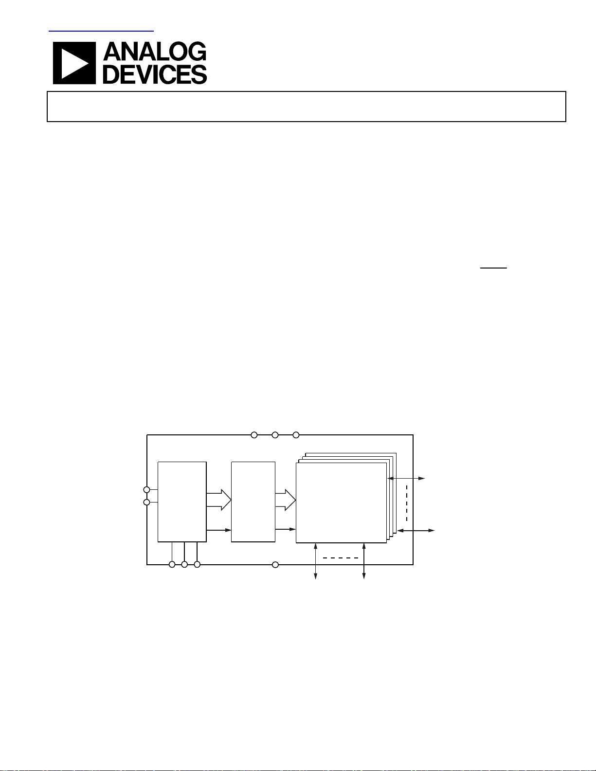
FUNCTIONAL BLOCK DIAGRAM
L
ADG2128
GNDA0A1A2
1
96
LDSW
Figure 1.
8 × 12 SWITCH ARRAY
Y0 TO Y7 (I/O)
X0 TO X11 (I/O)
05464-001
SCL
SD
INPUT
REGISTER
AND
7 TO 96
DECODER
1
LATCHES
96
LDSW
Rev. A
Information furnished by Analog Devices is believed to be accurate and reliable. However, no
responsibility is assumed by Anal og Devices for its use, nor for any infringements of patents or ot her
rights of third parties that may result from its use. Specifications subject to change without notice. No
license is granted by implication or otherwise under any patent or patent rights of Analog Devices.
Trademarks and registered trademarks are the property of their respective owners.
One Technology Way, P.O. Box 9106, Norwood, MA 02062-9106, U.S.A.
Tel: 781.329.4700 www.analog.com
Fax: 781.461.3113 ©2006 Analog Devices, Inc. All rights reserved.

ADG2128
TABLE OF CONTENTS
Features ..............................................................................1
Load Switch (LDSW).................................................18
Applications.......................................................................1
General Description.........................................................1
Functional Block Diagram ..............................................1
Revision History ...............................................................2
Specifications.....................................................................3
2
I
C Timing Specifications............................................7
Timing Diagram ...........................................................8
Absolute Maximum Ratings............................................9
ESD Caution..................................................................9
Pin Configuration and Function Descriptions...........10
Typical Performance Characteristics ...........................11
Test Ci r c ui t s.....................................................................15
Te r mi n ol o g y ....................................................................17
Theory of Operation ......................................................18
RESET
/Power-On Reset ............................................18
Readback ..................................................................... 18
Serial Interface................................................................ 19
High Speed I
Serial Bus Address...................................................... 19
Writing to the ADG2128............................................... 20
Input Shift Register.................................................... 20
Write Operation ......................................................... 22
Read Operation ..........................................................22
Evaluation Board ............................................................ 24
Using the ADG2128 Evaluation Board................... 24
Power Supply ..............................................................24
Schematics...................................................................25
Outline Dimensions....................................................... 27
Ordering Guide.......................................................... 27
2
C Interface........................................... 19
REVISION HISTORY
5/06—Rev. 0 to Rev. A
Added I
Changes to Table 1............................................................................ 3
Changes to Table 2............................................................................ 5
Changes to Table 4............................................................................ 9
Changes to Figure 24...................................................................... 14
Changes to Terminology Section.................................................. 17
Changes to Figure 35...................................................................... 23
Changes to the Ordering Guide.................................................... 27
1/06—Revision 0: Initial Version
2
C Information......................................................Universal
Rev. A | Page 2 of 28
ADG2128
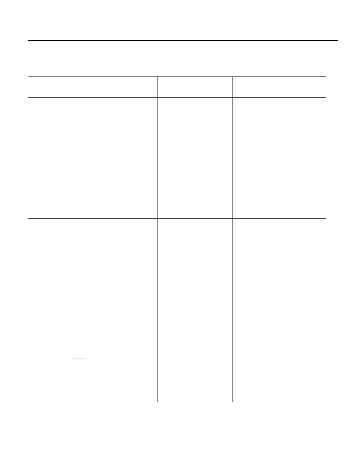
SPECIFICATIONS
VDD = 12 V ± 10%, VSS = 0 V, VL = 5 V, GND = 0 V, all specifications T
MIN
to T
unless otherwise noted.
MAX,
Table 1.
B Version Y Version
Parameter
+25°C
−40°C to
+85°C
+25°C
−40°C to
+125°C
Unit Conditions
ANALOG SWITCH
Analog Signal Range VDD − 2 V VDD − 2 V V max
On Resistance, R
ON
30 30 Ω typ VDD = +10.8 V, VIN = 0 V, IS = −10 mA
35 40 35 42 Ω max
32 32 Ω typ VDD = +10.8 V, VIN = +1.4 V, IS = −10 mA
37 42 37 47 Ω max
45 45 Ω typ VDD = +10.8 V, VIN = +5.4 V, IS = −10 mA
50 57 50 62 Ω max
On Resistance Matching 4.5 4.5 Ω typ VDD = +10.8 V, VIN = 0 V, IS = −10 mA
Between Channels, ∆R
On Resistance Flatness, R
ON
FLAT(ON)
8 9 8 10 Ω max
2.3 2.3 Ω typ VDD = 10.8 V, VIN = 0 V to +1.4 V, IS = −10 mA
3.5 4 3.5 5 Ω max
14.5 14.5 Ω typ VDD = 10.8 V, VIN = 0 V to +5.4 V, IS = −10 mA
18 20 18 22 Ω max
LEAKAGE CURRENTS VDD = 13.2 V
Channel Off Leakage, I
Channel On Leakage, I
OFF
ON
±0.03 ±0.03 μA typ VX = 7 V/1 V, VY = 1 V/7 V
±0.03 ±0.03 μA typ VX = VY = 1 V or 7 V
DYNAMIC CHARACTERISTICS2
C
OFF
11 11 pF typ
CON 18.5 18.5 pF typ
tON 170 170 ns typ RL = 300 Ω, CL = 35 pF
185 190 185 195 ns max
t
210 210 ns typ RL = 300 Ω, CL = 35 pF
OFF
250 255 250 260 ns max
THD + N 0.04 0.04 % typ
PSRR 90 dB typ
= 10 kΩ, f = 20 Hz to 20 kHz,
R
L
= 1 V p-p
V
S
f = 20 kHz; without decoupling;
see
−3 dB Bandwidth 210 210 MHz typ Individual inputs to outputs
16.5 16.5 MHz typ 8 inputs to 1 output
Off Isolation −69 −69 dB typ RL = 75 Ω, CL = 5 pF, f = 5 MHz
Channel-to-Channel Crosstalk RL = 75 Ω, CL = 5 pF, f = 5 MHz
Adjacent Channels −63 −63 dB typ
Nonadjacent Channels −76 −76 dB typ
Differential Gain 0.4 0.4 % typ RL = 75 Ω, CL = 5 pF, f = 5 MHz
Differential Phase 0.6 0.6 ° typ RL = 75 Ω, CL = 5 pF, f = 5 MHz
Charge Injection −3.5 −3.5 pC typ VS = 4 V, RS = 0 Ω, CL = 1 nF
LOGIC INPUTS (Ax, RESET)
Input High Voltage, V
Input Low Voltage, V
INL
Input Leakage Current, I
2
INH
IN
2.0 2.0 V min
0.8 0.8 V max
0.005 0.005 μA typ
±1 ±1 μA max
Input Capacitance, C
IN
7 7 pF typ
1
Figure 24
Rev. A | Page 3 of 28

ADG2128
B Version Y Version
Parameter
+25°C
+85°C
+25°C
LOGIC INPUTS (SCL, SDA)2
−40°C to
Input High Voltage, V
INH
V
Input Low Voltage, V
INL
0.3 V
Input Leakage Current, I
IN
0.7 V
+ 0.3 VL + 0.3 V max
L
L
0.7 V
−0.3 −0.3 V min
0.3 V
L
0.005 0.005 μA typ VIN = 0 V to VL
±1 ±1 μA max
Input Hysteresis 0.05 V
Input Capacitance, C
LOGIC OUTPUT (SDA)
Output Low Voltage, V
IN
2
OL
7 7 pF typ
0.4 0.4 V max I
0.05 V
L
0.6 0.6 V max I
Floating State Leakage Current ±1 ±1 μA max
POWER REQUIREMENTS
IDD 0.05 0.05 μA typ Digital inputs = 0 V or V
1 1 μA max
ISS 0.05 0.05 μA typ Digital inputs = 0 V or V
1 1 μA max
IL Digital inputs = 0 V or V
Interface Inactive 0.3 0.3 μA typ
2 2 μA max
Interface Active: 400 kHz f
0.1 0.1 mA typ
SCL
0.2 0.2 mA max
Interface Active: 3.4 MHz f
0.4 0.4 mA typ -HS model only
SCL
1.2 1.7 mA max
1
Temperature range is as follows: B version: −40°C to +85°C; Y version: −40°C to +125°C.
2
Guaranteed by design, not subject to production test.
−40°C to
+125°C
L
L
L
Unit Conditions
V min
V max
V min
= 3 mA
SINK
= 6 mA
SINK
L
L
L
Rev. A | Page 4 of 28
ADG2128
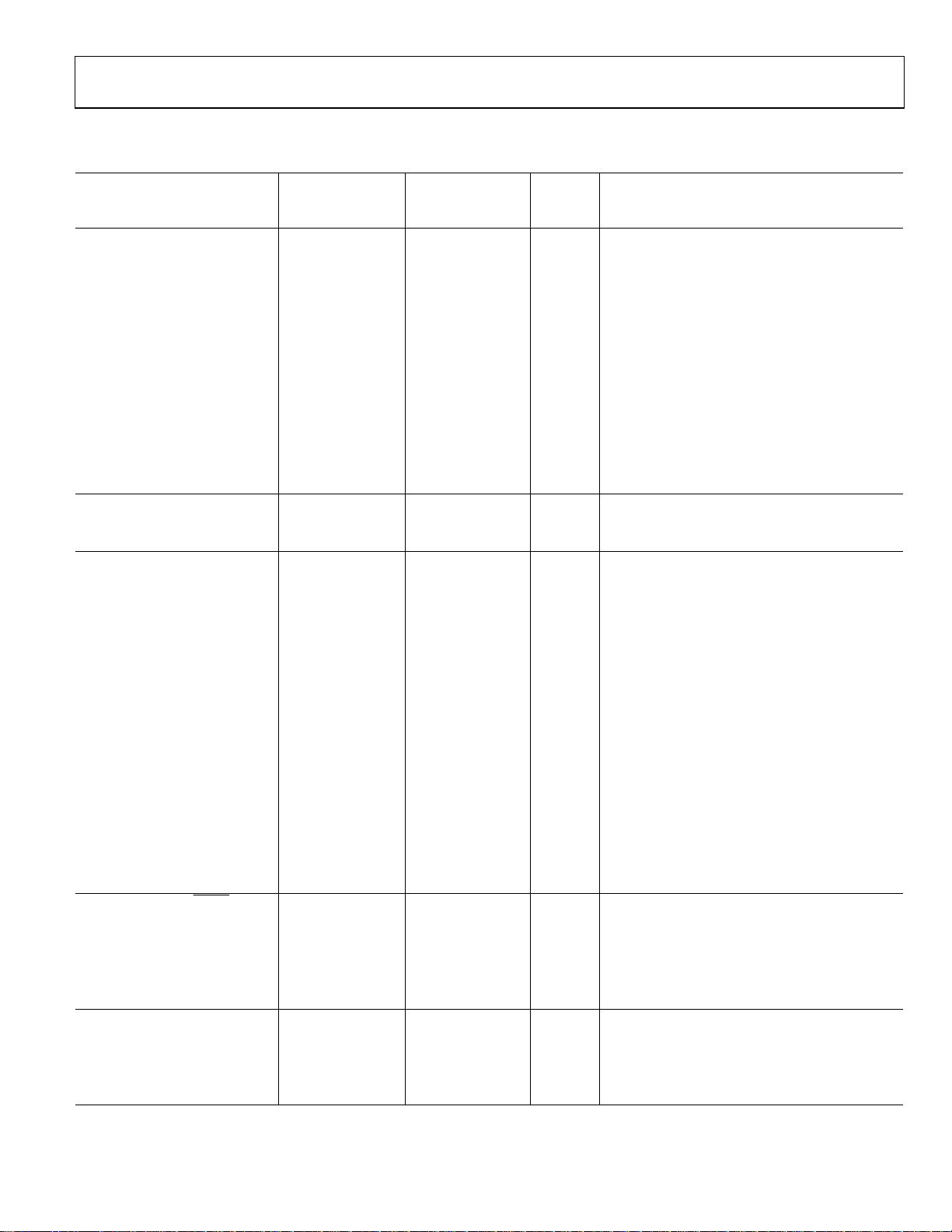
VDD = +5 V ± 10%, VSS = −5 V ± 10%, VL = 5 V, GND = 0 V, all specifications T
MIN
to T
, unless otherwise noted.
MAX
Table 2.
B Version Y Version
−40°C to
Parameter +25°C
+125°C
+25°C
−40°C to
+125°C
Unit Conditions
ANALOG SWITCH
Analog Signal Range VDD − 2 V V max
On Resistance, R
ON
34 34 Ω typ VDD = +4.5 V, VSS = −4.5 V, VIN = VSS, IS = −10 mA
40 45 40 50 Ω max
50 50 Ω typ VDD = +4.5 V, VSS = −4.5 V, VIN = 0 V, IS = −10 mA
55 65 55 70 Ω max
66 66 Ω typ VDD = +4.5 V, VSS = −4.5 V, VIN = +1.4 V, IS = −10 mA
75 85 75 95 Ω max
On Resistance Matching 4.5 4.5 Ω typ VDD = +4.5 V, VSS = −4.5 V, VIN = VSS, IS = −10 mA
Between Channels, ∆R
On Resistance Flatness, R
FLAT(ON)
8 9 8 10 Ω max
ON
17 17 Ω typ VDD = +4.5 V, VSS = −4.5 V, VIN = VSS to 0 V, IS = −10 mA
20 23 20 25 Ω max
34 34 Ω typ VDD = +4.5 V, VSS = −4.5 V, VIN = VSS to +1.4 V, IS = −10 mA
42 45 42 48 Ω max
LEAKAGE CURRENTS VDD = 5.5 V, VSS = 5.5 V
Channel Off Leakage, I
Channel On Leakage, I
OFF
ON
DYNAMIC CHARACTERISTICS
C
OFF
±0.03 ±0.03 μA typ VX = +4.5 V/−2 V, VY = −2 V/+4.5 V
±0.03 ±0.03 μA typ VX = VY = −2 V or +4.5 V
2
6 6 pF typ
CON 9.5 9.5 pF typ
tON 170 170 ns typ RL = 300 Ω, CL = 35 pF
200 215 200 220 ns max
t
210 210 ns typ RL = 300 Ω, CL = 35 pF
OFF
250 255 250 260 ns max
THD + N 0.04 0.04 % typ RL = 10 kΩ, f = 20 Hz to 20 kHz, VS = 1 V p-p
PSRR 90 dB typ f = 20 kHz; without decoupling; see Figure 24
−3 dB Bandwidth 300 300 MHz typ Individual inputs to outputs
18 18 MHz typ 8 inputs to 1 output
Off Isolation −66 −64 dB typ RL = 75 Ω, CL = 5 pF, f = 5 MHz
Channel-to-Channel Crosstalk RL = 75 Ω, CL = 5 pF, f = 5 MHz
Adjacent Channels −62 −62 dB typ
Nonadjacent Channels −79 −79 dB typ
Differential Gain 1.5 1.5 % typ RL = 75 Ω, CL = 5 pF, f = 5 MHz
Differential Phase 1.8 1.8 ° typ RL = 75 Ω, CL = 5 pF, f = 5 MHz
Charge Injection −3 −3 pC typ VS = 0 V, RS = 0 Ω, CL = 1 nF
LOGIC INPUTS (Ax, RESET)
Input High Voltage, V
Input Low Voltage, V
INL
Input Leakage Current, I
2
2.0 2.0 V min
INH
0.8 0.8 V max
IN
0.005 0.005 μA typ
±1 ±1 μA max
Input Capacitance, CIN 7 7 pF typ
LOGIC INPUTS (SCL, SDA)2
Input High Voltage, V
V
Input Low Voltage, V
0.3 V
0.7 V
INH
+ 0.3 VL + 0.3 V max
L
−0.3 −0.3 V min
INL
L
L
0.7 V
0.3 V
L
L
V min
V max
1
Rev. A | Page 5 of 28

ADG2128
Parameter +25°C
B Version Y Version
−40°C to
+125°C
+25°C
−40°C to
+125°C
Input Leakage Current, IIN 0.005 0.005 μA typ VIN = 0 V to VL
±1 ±1 μA max
Input Hysteresis 0.05 V
0.05 V
L
Input Capacitance, CIN 7 7 pF typ
LOGIC OUTPUT (SDA)
Output Low Voltage, V
2
OL
0.4 0.4 V max I
0.6 0.6 V max I
Floating State Leakage Current ±1 ±1 μA max
POWER REQUIREMENTS
IDD 0.05 0.005 μA typ Digital inputs = 0 V or V
1 1 μA max
ISS 0.05 0.005 μA typ Digital inputs = 0 V or V
1 1 μA max
IL Digital inputs = 0 V or V
Interface Inactive 0.3 0.3 μA typ
2 2 μA max
Interface Active: 400 kHz f
0.1 0.1 mA typ
SCL
0.1 0.1 mA max
Interface Active: 3.4 MHz f
0.4 0.4 mA typ -HS model only
SCL
0.3 0.3 mA max
1
Temperature range is as follows: B version: –40°C to +85°C; Y version: –40°C to +125°C.
2
Guaranteed by design, not subject to production test.
Unit Conditions
V min
L
= 3 mA
SINK
= 6 mA
SINK
L
L
L
Rev. A | Page 6 of 28

ADG2128
I2C TIMING SPECIFICATIONS
VDD = 5 V to 12 V; VSS = −5 V to 0 V; VL = 5 V; GND = 0 V; TA = T
Table 3.
ADG2108 Limit at T
Parameter1Conditions Min Max Unit Description
f
Standard mode 100 kHz Serial clock frequency
SCL
Fast mode 400 kHz
High speed mode
C
C
= 100 pF maximum 3.4 MHz
B
= 400 pF maximum 1.7 MHz
B
2
t1 Standard mode 4 μs t
Fast mode 0.6 μs
High speed mode
C
C
= 100 pF maximum 60 ns
B
= 400 pF maximum 120 ns
B
2
t2 Standard mode 4.7 μs t
Fast mode 1.3 μs
High speed mode
C
C
= 100 pF maximum 160 ns
B
= 400 pF maximum 320 ns
B
2
t3 Standard mode 250 ns t
Fast mode 100 ns
High speed mode
3
t
Standard mode 0 3.45 μs t
4
2
10 ns
Fast mode 0 0.9 μs
High speed mode
C
C
= 100 pF maximum 0 70 ns
B
= 400 pF maximum 0 150 ns
B
2
t5 Standard mode 4.7 μs t
Fast mode 0.6 μs
High speed mode
2
160 ns
t6 Standard mode 4 μs t
Fast mode 0.6 μs
High speed mode
2
160 ns
t7 Standard mode 4.7 μs t
Fast mode 1.3 μs
t8 Standard mode 4 μs t
Fast mode 0.6 μs
High speed mode
2
160 ns
t9 Standard mode 1000 ns t
Fast mode 20 + 0.1 CB B 300 ns
High speed mode
C
C
= 100 pF maximum 10 80 ns
B
= 400 pF maximum 20 160 ns
B
2
t10 Standard mode 300 ns t
Fast mode 20 + 0.1 C
High speed mode
C
C
= 100 pF maximum 10 80 ns
B
= 400 pF maximum 20 160 ns
B
2
B 300 ns
B
Rev. A | Page 7 of 28
MIN
, T
to T
MIN
MAX
MAX
, unless otherwise noted (see Figure 2).
, SCL high time
HIGH
, SCL low time
LOW
, data setup time
SU;DAT
, data hold time
HD;DAT
, setup time for a repeated start condition
SU;STA
, hold time for a repeated start condition
HD;STA
, bus free time between a stop and a start condition
BUF
, setup time for a stop condition
SU;STO
, rise time of SDA signal
RDA
, fall time of SDA signal
FDA
ADG2128
ADG2108 Limit at T
Parameter1Conditions Min Max Unit Description
t11 Standard mode 1000 ns t
Fast mode 20 + 0.1 C
High speed mode
C
C
t
Standard mode 1000 ns t
11A
= 100 pF maximum 10 40 ns
B
= 400 pF maximum 20 80 ns
B
2
B 300 ns
B
Fast mode 20 + 0.1 CB B 300 ns condition and after an acknowledge bit
High speed mode
C
C
= 100 pF maximum 10 80 ns
B
= 400 pF maximum 20 160 ns
B
2
t12 Standard mode 300 ns t
Fast mode 20 + 0.1 C
High speed mode
C
C
= 100 pF maximum 10 40 ns
B
= 400 pF maximum 20 80 ns
B
2
B 300 ns
B
tSP Fast mode 0 50 ns Pulse width of suppressed spike
High speed mode
1
Guaranteed by initial characterization. All values measured with input filtering enabled. CB refers to capacitive load on the bus line; tR and tF are measured between
0.3 VDD and 0.7 VDD.
2
High speed I2C is available only in -HS models.
3
A device must provide a data hold time for SDA to bridge the undefined region of the SCL falling edge.
2
0 10 ns
MIN
, T
MAX
, rise time of SCL signal
RCL
, rise time of SCL signal after a repeated start
RCL1
, fall time of SCL signal
FCL
TIMING DIAGRAM
SCL
SDA
t
7
P
S = START CONDITION
P = STOP CO NDITION
t
11
t
2
t
6
S
t
4
t
12
t
3
t
1
S
t
6
t
5
t
10
t
8
t
9
P
05464-002
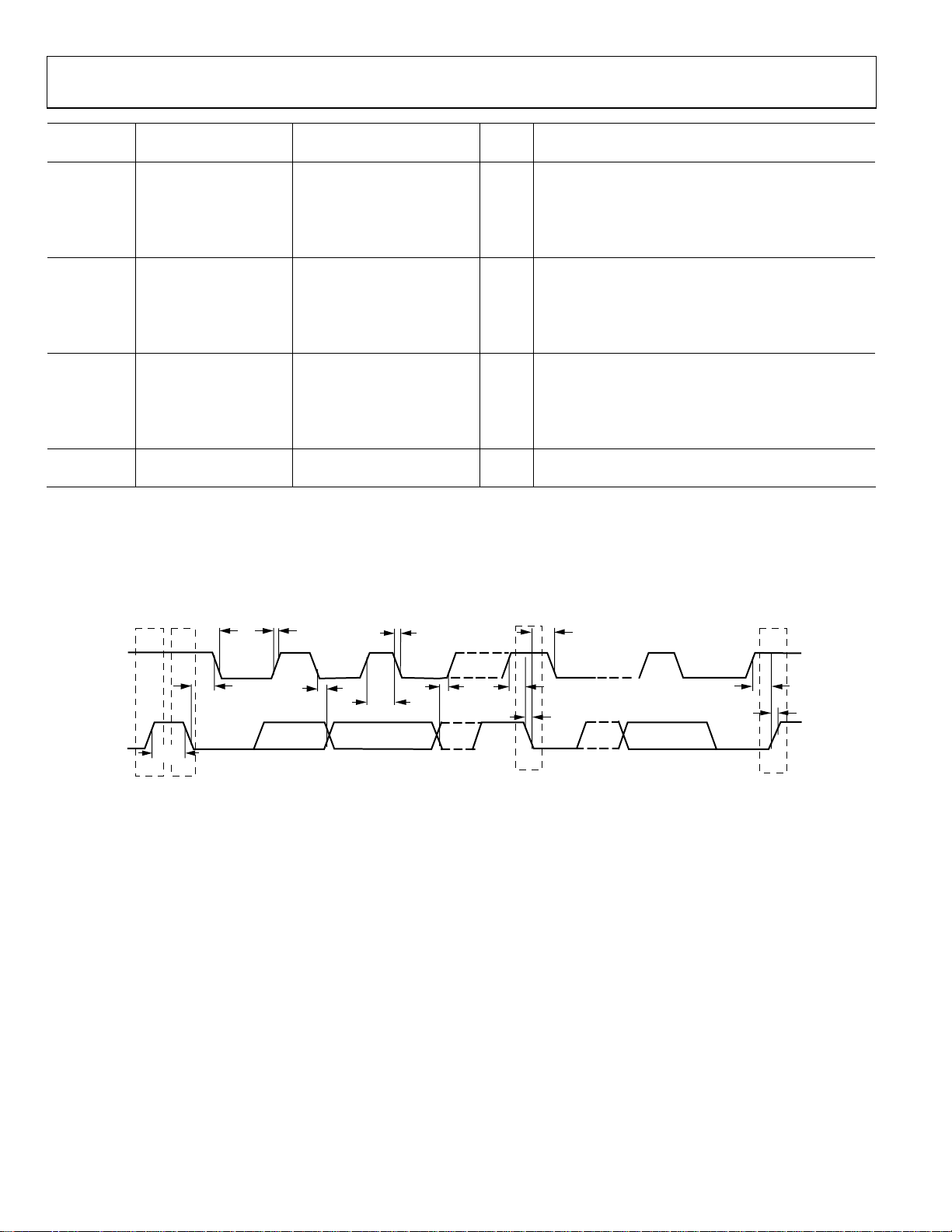
Figure 2. Timing Diagram for 2-Wire Serial Interface
Rev. A | Page 8 of 28
ADG2128
ABSOLUTE MAXIMUM RATINGS
TA = 25°C, unless otherwise noted.
Table 4.
Parameter Rating
VDD to VSS 15 V
VDD to GND −0.3 V to +15 V
VSS to GND +0.3 V to −7 V
VL to GND −0.3 V to +7 V
Analog Inputs VSS − 0.3 V to VDD + 0.3 V
Digital Inputs
Continuous Current
10 V on Input; Single Input
Connected to Single Output
1 V on Input; Single Input
Connected to Single Output
10 V on Input; Eight Inputs
Connected to Eight Outputs
Operating Temperature Range
Industrial (B Version) –40°C to +85°C
Automotive (Y Version) –40°C to +125°C
Storage Temperature Range –65°C to +150°C
Junction Temperature 150°C
32-Lead LFCSP_VQ
θJA Thermal Impedance 108.2°C/W
Reflow Soldering (Pb Free)
Peak Temperature 260°C (+0/–5)
Time at Peak Temperature 10 sec to 40 sec
−0.3 V to V
whichever occurs first
65 mA
90 mA
25 mA
+ 0.3 V or 30 mA,
L
Stresses above those listed under Absolute Maximum Ratings
may cause permanent damage to the device. This is a stress
rating only; functional operation of the device at these or any
other conditions above those indicated in the operational
section of this specification is not implied. Exposure to absolute
maximum rating conditions for extended periods may affect
device reliability.
ESD CAUTION
ESD (electrostatic discharge) sensitive device. Electrostatic charges as high as 4000 V readily accumulate on
the human body and test equipment and can discharge without detection. Although this product features
proprietary ESD protection circuitry, permanent damage may occur on devices subjected to high energy
electrostatic discharges. Therefore, proper ESD precautions are recommended to avoid performance
degradation or loss of functionality.
Rev. A | Page 9 of 28
 Loading...