

VDDVSSV
A
查询ADG2108供应商
I2C® CMOS 8 × 10 Unbuffered Analog
FEATURES
I2C-compatible interface
3.4 MHz high speed I
32-lead LFCSP_VQ (5 mm × 5 mm)
Double-buffered input logic
Simultaneous update of multiple switches
Up to 300 MHz bandwidth
Fully specified at dual ±5 V/single +12 V operation
On resistance 35 Ω maximum
Low quiescent current < 20 μA
APPLICATIONS
AV switching in TV
Automotive infotainment
AV receivers
CCT V
Ultrasound applications
KVM switching
Telecom applications
Test equipment/instrumentation
PBX systems
2
C option
Switch Array with Dual/Single Supplies
ADG2108
GENERAL DESCRIPTION
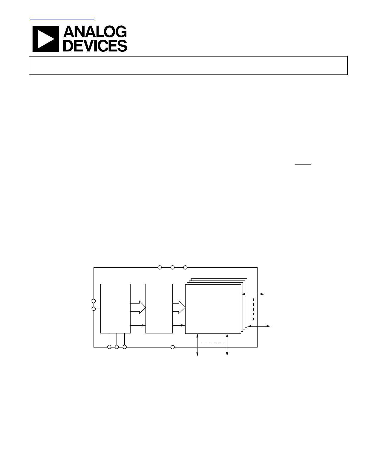
The ADG2108 is an analog cross point switch with an
array size of 8 × 10. The switch array is arranged so that
there are eight columns by 10 rows, for a total of 80 switch
channels. The array is bidirectional, and the rows and columns
can be configured as either inputs or outputs. Each of the 80
switches can be addressed and configured through the I
compatible interface. Standard, full speed, and high speed
(3.4 MHz) I
2
C interfaces are supported. Any simultaneous
switch combination is allowed. An additional feature of the
ADG2108 is that switches can be updated simultaneously,
using the LDSW command. In addition, a
RESET
allows all of the switch channels to be reset/off. At power on,
all switches are in the off condition. The device is packaged
in a 32-lead, 5 mm × 5 mm LFCSP_VQ.
2
C-
option
FUNCTIONAL BLOCK DIAGRAM
ADG2108
SCL
SD
INPUT
REGISTER
AND
7 TO 80
DECODER
Rev. 0
Information furnished by Analog Devices is believed to be accurate and reliable. However, no
responsibility is assumed by Anal og Devices for its use, nor for any infringements of patents or ot her
rights of third parties that may result from its use. Specifications subject to change without notice. No
license is granted by implication or otherwise under any patent or patent rights of Analog Devices.
Trademarks and registered trademarks are the property of their respective owners.
1
80
LDSW
LATCHES
LDSW
GNDA0A1A2
1
80
Figure 1.
L
8 × 10 SWITCH ARRAY
Y0 TO Y7 (I/O)
One Technology Way, P.O. Box 9106, Norwood, MA 02062-9106, U.S.A.
Tel: 781.329.4700 www.analog.com
Fax: 781.461.3113 ©2006 Analog Devices, Inc. All rights reserved.
X0 TO X9 (I/O)
5898-001

ADG2108
TABLE OF CONTENTS
Features.............................................................................................. 1
Load Switch (LDSW)................................................................. 18
Applications....................................................................................... 1
General Description ......................................................................... 1
Functional Block Diagram .............................................................. 1
Revision History ............................................................................... 2
Specifications..................................................................................... 3
2
I
C Timing Specifications............................................................ 7
Timing Diagram........................................................................... 8
Absolute Maximum Ratings............................................................ 9
ESD Caution.................................................................................. 9
Pin Configuration and Function Descriptions........................... 10
Typical Performance Characteristics ........................................... 11
Test Circuits..................................................................................... 15
Terminology .................................................................................... 17
Theory of Operation ...................................................................... 18
RESET
/Power-On Reset ............................................................18
Readback ..................................................................................... 18
Serial Interface ................................................................................ 19
High Speed I
Serial Bus Address...................................................................... 19
Writing to the ADG2108............................................................... 20
Input Shift Register .................................................................... 20
Write Operation.......................................................................... 22
Read Operation........................................................................... 22
Evaluation Board............................................................................ 24
Using the ADG2108 Evaluation Board ................................... 24
Power Supply............................................................................... 24
Schematics................................................................................... 25
Outline Dimensions....................................................................... 27
Ordering Guide .......................................................................... 27
2
C Interface........................................................... 19
REVISION HISTORY
4/06—Revision 0: Initial Version
Rev. 0 | Page 2 of 28

ADG2108
SPECIFICATIONS
VDD = 12 V ± 10%, VSS = 0 V, VL = 5 V, GND = 0 V, all specifications T
MIN
to T
unless otherwise noted.
MAX,
Table 1.
B Version Y Version
Parameter
+25°C
−40°C to
+85°C
+25°C
−40°C to
+125°C
Unit Conditions
ANALOG SWITCH
Analog Signal Range VDD − 2 V VDD − 2 V V max
On Resistance, RON 30 30 Ω typ VDD = 10.8 V, VIN = 0 V, IS = −10 mA
35 40 35 42 Ω max
32 32 Ω typ VDD = 10.8 V, VIN = 1.4 V, IS = −10 mA
37 42 37 47 Ω max
45 45 Ω typ VDD = 10.8 V, VIN = 5.4 V, IS = −10 mA
50 57 50 62 Ω max
On Resistance Matching 4.5 4.5 Ω typ VDD = 10.8 V, VIN = 0 V, IS = −10 mA
Between Channels, ∆RON 8 9 8 10 Ω max
On Resistance Flatness, R
2.3 2.3 Ω typ VDD = 10.8 V, VIN = 0 V to 1.4 V, IS = −10 mA
FLAT(ON)
3.5 4 3.5 5 Ω max
14.5 14.5 Ω typ VDD = 10.8 V, VIN = 0 V to 5.4 V, IS = −10 mA
18 20 18 22 Ω max
LEAKAGE CURRENTS VDD = 13.2 V
Channel Off Leakage, I
±0.03 ±0.03 μA typ VX = 7 V/1 V, VY = 1 V/7 V
OFF
Channel On Leakage, ION ±0.03 ±0.03 μA typ VX = VY = 1 V or 7 V
DYNAMIC CHARACTERISTICS2
C
11 11 pF typ
OFF
CON 18.5 18.5 pF typ
tON 170 170 ns typ RL = 300 Ω, CL = 35 pF
185 190 185 195 ns max
t
210 210 ns typ RL = 300 Ω, CL = 35 pF
OFF
250 255 250 260 ns max
THD + N 0.04 0.04 % typ
PSRR 90 dB typ
= 10 kΩ, f = 20 Hz to 20 kHz,
R
L
= 1 V p-p
V
S
f = 20 kHz; without decoupling;
see
−3 dB Bandwidth 210 210 MHz typ Individual inputs to outputs
16.5 16.5 MHz typ 8 inputs to 1 output
Off Isolation −69 −69 dB typ RL = 75 Ω, CL = 5 pF, f = 5 MHz
Channel-to-Channel Crosstalk RL = 75 Ω, CL = 5 pF, f = 5 MHz
Adjacent Channels −63 −63 dB typ
Nonadjacent Channels −76 −76 dB typ
Differential Gain 0.4 0.4 % typ RL = 75 Ω, CL = 5 pF, f = 5 MHz
Differential Phase 0.6 0.6 ° typ RL = 75 Ω, CL = 5 pF, f = 5 MHz
Charge Injection −3.5 −3.5 pC typ VS = 4 V, RS = 0 Ω, CL = 1 nF
LOGIC INPUTS (Ax, RESET)
Input High Voltage, V
Input Low Voltage, V
INL
2
2.0 2.0 V min
INH
0.8 0.8 V max
Input Leakage Current, IIN 0.005 0.005 μA typ
±1 ±1 μA max
Input Capacitance, CIN 7 7 pF typ
1
Figure 24
Rev. 0 | Page 3 of 28

ADG2108
B Version Y Version
Parameter
+25°C
+85°C
+25°C
LOGIC INPUTS (SCL, SDA)2
−40°C to
Input High Voltage, V
V
Input Low Voltage, V
0.7 VL 0.7 VL V min
INH
+ 0.3 VL + 0.3 V max
L
−0.3 −0.3 V min
INL
0.3 VL 0.3 VL V max
Input Leakage Current, IIN 0.005 0.005 μA typ VIN = 0 V to VL
±1 ±1 μA max
Input Hysteresis 0.05 VL 0.05 VL V min
Input Capacitance, CIN 7 7 pF typ
LOGIC OUTPUT (SDA)
2
Output Low Voltage, VOL 0.4 0.4 V max I
0.6 0.6 V max I
Floating State Leakage Current ±1 ±1 μA max
POWER REQUIREMENTS
IDD 0.05 0.05 μA typ Digital inputs = 0 V or VL
1 1 μA max
ISS 0.05 0.05 μA typ Digital inputs = 0 V or VL
1 1 μA max
IL Digital inputs = 0 V or VL
Interface Inactive 0.3 0.3 μA typ
2 2 μA max
Interface Active: 400 kHz f
0.1 0.1 mA typ
SCL
0.2 0.2 mA max
Interface Active: 3.4 MHz f
0.4 0.4 mA typ -HS model only
SCL
1.2 1.7 mA max
1
Temperature range is as follows: B version: −40°C to +85°C; Y version: −40°C to +125°C.
2
Guaranteed by design, not subject to production test.
−40°C to
+125°C
Unit Conditions
= 3 mA
SINK
= 6 mA
SINK
Rev. 0 | Page 4 of 28

ADG2108
VDD = +5 V ± 10%, VSS = −5 V ± 10%, VL = 5 V, GND = 0 V, all specifications T
MIN
to T
, unless otherwise noted.
MAX
Table 2.
B Version Y Version
−40°C to
Parameter +25°C
+125°C
+25°C
−40°C to
+125°C
Unit Conditions
ANALOG SWITCH
Analog Signal Range VDD − 2 V V max
On Resistance, RON 34 34 Ω typ VDD = +4.5 V, VSS = −4.5 V, VIN = VSS, IS = −10 mA
40 45 40 50 Ω max
50 50 Ω typ VDD = +4.5 V, VSS = −4.5 V, VIN = 0 V, IS = −10 mA
55 65 55 70 Ω max
66 66 Ω typ VDD = +4.5 V, VSS = −4.5 V, VIN = 1.4 V, IS = −10 mA
75 85 75 95 Ω max
On Resistance Matching 4.5 4.5 Ω typ VDD = +4.5 V, VSS = −4.5 V, VIN = VSS, IS = −10 mA
Between Channels, ∆RON 8 9 8 10 Ω max
On Resistance Flatness, R
17 17 Ω typ VDD = +4.5 V, VSS = −4.5 V, VIN = VSS to 0 V, IS = −10 mA
FLAT(ON)
20 23 20 25 Ω max
34 34 Ω typ VDD = +4.5 V, VSS = −4.5 V, VIN = VSS to 1.4 V, IS = −10 mA
42 45 42 48 Ω max
LEAKAGE CURRENTS VDD = 5.5 V, VSS = 5.5 V
Channel Off Leakage, I
±0.03 ±0.03 μA typ VX = +4.5 V/−2 V, VY = −2 V/+4.5 V
OFF
Channel On Leakage, ION ±0.03 ±0.03 μA typ VX = VY = −2 V or +4.5 V
DYNAMIC CHARACTERISTICS
C
6 6 pF typ
OFF
2
CON 9.5 9.5 pF typ
tON 170 170 ns typ RL = 300 Ω, CL = 35 pF
200 215 200 220 ns max
t
210 210 ns typ RL = 300 Ω, CL = 35 pF
OFF
250 255 250 260 ns max
THD + N 0.04 0.04 % typ RL = 10 kΩ, f = 20 Hz to 20 kHz, VS = 1 V p-p
PSRR 90 dB typ f = 20 kHz; without decoupling; see Figure 24
−3 dB Bandwidth 300 300 MHz typ Individual inputs to outputs
18 18 MHz typ 8 inputs to 1 output
Off Isolation −66 −64 dB typ RL = 75 Ω, CL = 5 pF, f = 5 MHz
Channel-to-Channel Crosstalk RL = 75 Ω, CL = 5 pF, f = 5 MHz
Adjacent Channels −62 −62 dB typ
Nonadjacent Channels −79 −79 dB typ
Differential Gain 1.5 1.5 % typ RL = 75 Ω, CL = 5 pF, f = 5 MHz
Differential Phase 1.8 1.8 ° typ RL = 75 Ω, CL = 5 pF, f = 5 MHz
Charge Injection −3 −3 pC typ VS = 0 V, RS = 0 Ω, CL = 1 nF
LOGIC INPUTS (Ax, RESET)
Input High Voltage, V
Input Low Voltage, V
INL
2
2.0 2.0 V min
INH
0.8 0.8 V max
Input Leakage Current, IIN 0.005 0.005 μA typ
±1 ±1 μA max
Input Capacitance, CIN 7 7 pF typ
LOGIC INPUTS (SCL, SDA)2
Input High Voltage, V
V
Input Low Voltage, V
0.7 VL 0.7 VL V min
INH
+ 0.3 VL + 0.3 V max
L
−0.3 −0.3 V min
INL
0.3 VL 0.3 VL V max
1
Rev. 0 | Page 5 of 28

ADG2108
Parameter +25°C
B Version Y Version
−40°C to
+125°C
+25°C
−40°C to
+125°C
Input Leakage Current, IIN 0.005 0.005 μA typ VIN = 0 V to VL
±1 ±1 μA max
Input Hysteresis 0.05 VL 0.05 VL V min
Input Capacitance, CIN 7 7 pF typ
LOGIC OUTPUT (SDA)
2
Output Low Voltage, VOL 0.4 0.4 V max I
0.6 0.6 V max I
Floating State Leakage Current ±1 ±1 μA max
POWER REQUIREMENTS
IDD 0.05 0.005 μA typ Digital inputs = 0 V or VL
1 1 μA max
ISS 0.05 0.005 μA typ Digital inputs = 0 V or VL
1 1 μA max
IL Digital inputs = 0 V or VL
Interface Inactive 0.3 0.3 μA typ
2 2 μA max
Interface Active: 400 kHz f
0.1 0.1 mA typ
SCL
0.1 0.1 mA max
Interface Active: 3.4 MHz f
0.4 0.4 mA typ -HS model only
SCL
0.3 0.3 mA max
1
Temperature range is as follows: B version: –40°C to +85°C; Y version: –40°C to +125°C.
2
Guaranteed by design, not subject to production test.
Unit Conditions
= 3 mA
SINK
= 6 mA
SINK
Rev. 0 | Page 6 of 28

ADG2108
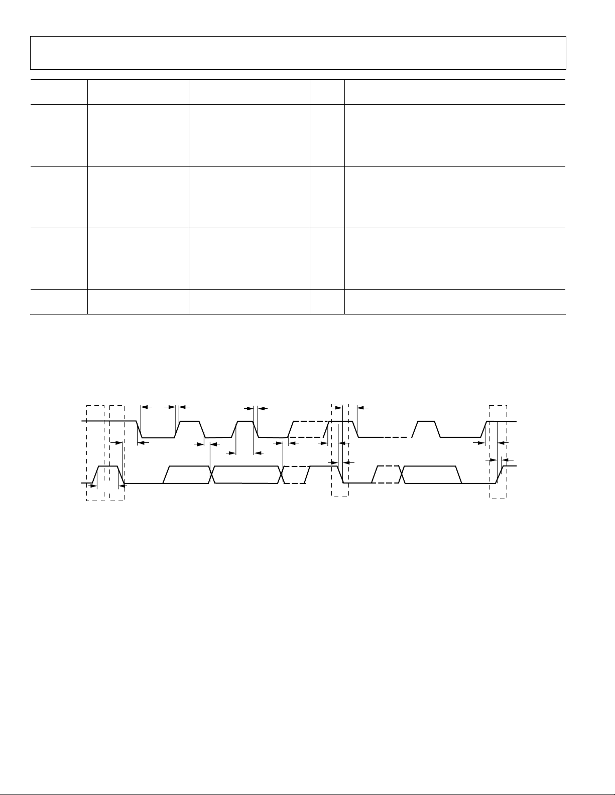
I2C TIMING SPECIFICATIONS
VDD = 5 V to 12 V; VSS = −5 V to 0 V; VL = 5 V; GND = 0 V; TA = T
Table 3.
ADG2108 Limit at T
Parameter1Conditions Min Max Unit Description
f
Standard mode 100 kHz Serial clock frequency
SCL
Fast mode 400 kHz
High speed mode
C
C
= 100 pF maximum 3.4 MHz
B
= 400 pF maximum 1.7 MHz
B
2
t1 Standard mode 4 μs t
Fast mode 0.6 μs
High speed mode
C
C
= 100 pF maximum 60 ns
B
= 400 pF maximum 120 ns
B
2
t2 Standard mode 4.7 μs t
Fast mode 1.3 μs
High speed mode
C
C
= 100 pF maximum 160 ns
B
= 400 pF maximum 320 ns
B
2
t3 Standard mode 250 ns t
Fast mode 100 ns
High speed mode
3
t
Standard mode 0 3.45 μs t
4
2
10 ns
Fast mode 0 0.9 μs
High speed mode
C
C
= 100 pF maximum 0 70 ns
B
= 400 pF maximum 0 150 ns
B
2
t5 Standard mode 4.7 μs t
Fast mode 0.6 μs
High speed mode
2
160 ns
t6 Standard mode 4 μs t
Fast mode 0.6 μs
High speed mode
2
160 ns
t7 Standard mode 4.7 μs t
Fast mode 1.3 μs
t8 Standard mode 4 μs t
Fast mode 0.6 μs
High speed mode
2
160 ns
t9 Standard mode 1000 ns t
Fast mode 20 + 0.1 CB 300 ns
High speed mode
C
C
= 100 pF maximum 10 80 ns
B
= 400 pF maximum 20 160 ns
B
2
t10 Standard mode 300 ns t
Fast mode 20 + 0.1 CB 300 ns
High speed mode
C
C
= 100 pF maximum 10 80 ns
B
= 400 pF maximum 20 160 ns
B
2
Rev. 0 | Page 7 of 28
MIN
to T
MIN
, T
MAX
, unless otherwise noted (see Figure 2).
MAX
, SCL high time
HIGH
, SCL low time
LOW
, data setup time
SU;DAT
, data hold time
HD;DAT
, setup time for a repeated start condition
SU;STA
, hold time for a repeated start condition
HD;STA
, bus free time between a stop and a start condition
BUF
, setup time for a stop condition
SU;STO
, rise time of SDA signal
RDA
, fall time of SDA signal
FDA
ADG2108
ADG2108 Limit at T
Parameter1Conditions Min Max Unit Description
t11 Standard mode 1000 ns t
Fast mode 20 + 0.1 CB 300 ns
High speed mode
C
C
t
Standard mode 1000 ns t
11A
= 100 pF maximum 10 40 ns
B
= 400 pF maximum 20 80 ns
B
2
Fast mode 20 + 0.1 CB 300 ns condition and after an acknowledge bit
High speed mode
C
C
= 100 pF maximum 10 80 ns
B
= 400 pF maximum 20 160 ns
B
2
t12 Standard mode 300 ns t
Fast mode 20 + 0.1 CB 300 ns
High speed mode
C
C
= 100 pF maximum 10 40 ns
B
= 400 pF maximum 20 80 ns
B
2
tSP Fast mode 0 50 ns Pulse width of suppressed spike
High speed mode
1
Guaranteed by initial characterization. All values measured with input filtering enabled. CB refers to capacitive load on the bus line; tR and tF are measured between
0.3 VDD and 0.7 VDD.
2
High speed I2C is available only in -HS models.
3
A device must provide a data hold time for SDA to bridge the undefined region of the SCL falling edge.
2
0 10 ns
MIN
, T
MAX
, rise time of SCL signal
RCL
, rise time of SCL signal after a repeated start
RCL1
, fall time of SCL signal
FCL
TIMING DIAGRAM
SCL
SDA
t
7
S
P
S = START CONDI TION
P = STOP CO NDITION
t
11
t
2
t
6
t
4
t
12
t
3
t
1
S
t
6
t
5
t
10
t
8
t
9
P
5898-002
Figure 2. Timing Diagram for 2-Wire Serial Interface
Rev. 0 | Page 8 of 28
ADG2108
ABSOLUTE MAXIMUM RATINGS
TA = 25°C, unless otherwise noted.
Table 4.
Parameter Rating
VDD to VSS 15 V
VDD to GND −0.3 V to +15 V
VSS to GND +0.3 V to −7 V
VL to GND −0.3 V to +7 V
Analog Inputs VSS − 0.3 V to VDD + 0.3 V
Digital Inputs
Continuous Current
10 V on Input; Single Input
Connected to Single Output
1 V on Input; Single Input
Connected to Single Output
10 V on Input; Eight Inputs
Connected to Eight Outputs
Operating Temperature Range
Industrial (B Version) –40°C to +85°C
Automotive (Y Version) –40°C to +125°C
Storage Temperature Range –65°C to +150°C
Junction Temperature 150°C
32-Lead LFCSP_VQ
θJA Thermal Impedance 108.2°C/W
Reflow Soldering (Pb Free)
Peak Temperature 260°C (+0/–5)
Time at Peak Temperature 10 sec to 40 sec
−0.3 V to V
whichever occurs first
65 mA
90 mA
25 mA
+ 0.3 V or 30 mA,
L
Stresses above those listed under Absolute Maximum Ratings
may cause permanent damage to the device. This is a stress
rating only; functional operation of the device at these or any
other conditions above those indicated in the operational
section of this specification is not implied. Exposure to absolute
maximum rating conditions for extended periods may affect
device reliability.
ESD CAUTION
ESD (electrostatic discharge) sensitive device. Electrostatic charges as high as 4000 V readily accumulate on
the human body and test equipment and can discharge without detection. Although this product features
proprietary ESD protection circuitry, permanent damage may occur on devices subjected to high energy
electrostatic discharges. Therefore, proper ESD precautions are recommended to avoid performance
degradation or loss of functionality.
Rev. 0 | Page 9 of 28

ADG2108
V
PIN CONFIGURATION AND FUNCTION DESCRIPTIONS
SS
NC
NC
NC
X0
X1
X2
X3
NC = NO CONNECT
Exposed Paddle Soldered to V
Table 5. Pin Function Descriptions
1
Pin No. Mnemonic Description
1 VSS
Negative Power Supply in a Dual-Supply Application. For single-supply applications, this pin
should be tied to GND.
2 to 4, 23 NC No Connect.
5 to 8,
X0 to X9 Can be inputs or outputs.
17 to 22
9 to 16 Y0 to Y7 Can be inputs or outputs.
24 VDD Positive Power Supply Input.
25 VL Logic Power Supply Input.
26 SDA Digital I/O. Bidirectional open drain data line. External pull-up resistor required.
27 SCL
Digital Input, Serial Clock Line. Open drain input that is used in conjunction with SDA to clock data
into the device. External pull-up resistor required.
28 A0 Logic Input. Address pin that sets the least significant bit of the 7-bit slave address.
29 A1 Logic Input. Address pin that sets the second least significant bit of the 7-bit slave address.
30 A2 Logic Input. Address pin that sets the third least significant bit of the 7-bit slave address.
31
RESET
Active Low Logic Input. When this pin is low, all switches are open, and appropriate registers are cleared to 0.
32 GND Ground. Reference point for all circuitry on the ADG2108.
1
It is recommended that the exposed paddle be soldered to VSS to improve heat dissipation and crosstalk.
T
E
D
S
N
E
1
2
R
G
32 31 30 29 28 27 26 25
1
PIN 1
2
INDICATOR
3
4
5
6
7
8
9 1011 1314151612
1
0
Y
Y
0
A
A
A
ADG2108
10 × 8
TOP VIEW
(Not to Scale)
2
4
3
Y
Y
Y
Figure 3. Pin Configuration
L
A
C
D
L
S
S
V
24
V
DD
23
NC
22
X9
21
X8
20
X7
19
X6
18
X5
X4
17
6
7
5
Y
Y
Y
05898-003
SS
Rev. 0 | Page 10 of 28

ADG2108
TYPICAL PERFORMANCE CHARACTERISTICS
200
TA = 25°C
I
= 10mA
DS
180
160
= 0V
140
120
(Ω)
100
ON
R
80
60
40
20
0
–5 12
–4–3–2–101234567891011
VSS = –5V
V
= +5V
DD
SOURCE VOLT AGE (V)
V
SS
V
= +8V
DD
V
DD
Figure 4. Signal Range
85
TA = 25°C
= 10mA
I
DS
75
65
(Ω)
55
ON
R
45
35
VDD/VSS = ±4.5V
= ±5V
V
DD/VSS
V
DD/VSS
V
SS
= +12V
= 0V
= ±5.5V
05898-007
90
TA = 25°C
= 10mA
I
DS
80
70
(Ω)
60
ON
R
50
40
30
054.54.03.53.02.52.01.51. 00.5
SOURCE VOLTAGE (V)
Figure 7. RON vs. Source Voltage, VDD = 8 V ± 10%
80
VDD = +5V
V
= –5V
SS
70
I
= 10mA
DS
60
50
(Ω)
40
ON
R
30
20
10
TA = +85°C
= –40°C
T
A
V
DD
VDD = 8V
T
= +125°C
A
T
= 7.2V
= +25°C
A
= 8.8V
V
DD
.0
05898-025
25
–5.5 1.50.5–0.5–1.5–2.5–3.5–4.5
SOURCE VOLT AGE (V)
Figure 5. RON vs. Source Voltage, Dual ±5 V Supplies
70
TA = 25°C
65
= 10mA
I
DS
60
(Ω)
R
ON
55
50
45
40
35
30
25
20
087654321
Figure 6. R
SOURCE VOLTAGE (V)
vs. Supplies, VDD = 12 V ± 10%
ON
VDD = 12V
V
= 10.8V
DD
V
DD
= 13.2V
0
–5 10–1–2–3–4
05898-017
SOURCE VOLTAGE (V)
05898-026
Figure 8. RON vs. Temperature, Dual ±5 V Supplies
60
VDD = 12V
V
= 0V
SS
I
= 10mA
DS
50
40
(Ω)
30
ON
R
20
10
0
0654321
05898-018
Figure 9. R
SOURCE VOLTAGE (V)
vs. Temperature, VDD = 12 V
ON
T
A
= +85°C
= –40°C
T
A
TA = +125°C
T
= +25°C
A
05898-027
Rev. 0 | Page 11 of 28

ADG2108
80
VDD = 8V
V
= 0V
SS
70
I
= 10mA
DS
60
50
(Ω)
40
ON
R
30
20
10
0
0 0.5 1.0 1.5 2.0 2.5 3.0 3.5 4.0
= +85°C
T
A
= –40°C
T
A
SOURCE VOLT AGE (V)
TA = +125°C
= +25°C
T
A
Figure 10. RON vs. Temperature, VDD = 8 V
05898-013
18
VDD = 12V
V
= 0V
SS
16
14
12
10
8
6
4
LEAKAGE CURRENTS (nA)
2
0
–2
0 20406080100120
TEMPERATURE ( °C)
Y CHANNELS, V
X CHANNELS, V
Y CHANNELS, V
BIAS
BIAS
BIAS
= 1V
= 7V
Figure 13. On Leakage vs. Temperature, 12 V Single Supply
= 7V
05898-011
16
VDD = +5V
V
= –5V
SS
14
12
10
8
6
4
LEAKAGE CURRENTS (nA)
2
0
0 20406080100120
TEMPERATURE ( °C)
X CHANNELS,
V
= +4V
BIAS
Y CHANNELS,
V
= –2V
BIAS
Figure 11. On Leakage vs. Temperature, Dual ±5 V Supplies
12
VDD = +5V
V
= –5V
SS
10
8
6
4
2
LEAKAGE CURRENTS (nA)
0
–2
0 20406080100120
X, Y CHANNELS;
V
= +4V ON X CHANNEL;
BIAS
–2V ON Y CHANNEL
X, Y CHANNELS;
V
= –2V ON X CHANNEL;
BIAS
+4V ON Y CHANNEL
TEMPERATURE ( °C)
Figure 12. Off Leakage vs. Temperature, Dual ±5 V Supplies
9
VDD = 12V
V
= 0V
SS
8
7
6
5
4
3
2
LEAKAGE CURRENTS (nA)
1
0
–1
0 20406080100120
05898-014
X, Y CHANNELS;
V
= 7V ON X CHANNEL;
BIAS
1V ON Y CHANNEL
X, Y CHANNELS;
V
= 1V ON X CHANNEL;
BIAS
7V ON Y CHANNEL
TEMPERATURE ( °C)
05898-012
Figure 14. Off Leakage vs. Temperature, 12 V Single Supply
0
–0.5
–1.0
–1.5
–2.0
–2.5
–3.0
–3.5
VDD = +5V, VSS = –5V
CHARGE INJECTI ON (pC)
–4.0
–4.5
–5.0
05898-015
–3–5 –11357911
SUPPLY VOLTAGE (V)
= +12V, VSS = 0V
V
DD
05898-030
Figure 15. Charge Injection vs. Supply Voltage
Rev. 0 | Page 12 of 28

ADG2108
–
–
–
240
220
t
OFF
200
(ns)
180
OFF
t
t
/
ON
ON
160
t
140
120
100
–40 –20 0 20 40 60 80 100 120
Figure 16. t
2
–3
–4
–5
–6
INSERTION LOSS (dB)
–7
VDD = +5V
= –5V
V
SS
= 25°C
T
A
–8
10 1G 10G10M100k1k
V
= +5V, VSS = –5V
DD
VDD = 12V, VSS = 0V
TEMPERATURE
Times vs. Temperature
ON/tOFF
FREQUENCY (Hz)
(°C)
Figure 17. Individual Inputs to Individual Outputs Bandwidth,
Dual ±5 V Supply
1
–2
0
–1
–2
–3
–4
–5
INSERTION LOSS (dB)
–6
VDD = +5V
–7
V
= –5V
SS
= 25°C
T
A
–8
10 1G 10G10M100k1k
05898-029
FREQUENCY (Hz)
05898-022
Figure 19. One Input to Eight Outputs Bandwidth, ±5 V Dual Supply
10
VDD = +5V TO +12V
= –5V TO 0V
V
SS
–20
= 25°C
T
A
–30
–40
–50
–60
–70
–80
INSERTION LOSS (dB)
–90
–100
–110
10 1G10M100k1k
05898-020
FREQUENCY (Hz)
05898-023
Figure 20. Off Isolation vs. Frequency
VDD = +5V TO +12V
V
= –5V TO 0V
–20
SS
T
= 25°C
A
–3
–4
–5
INSERTION LOSS (dB)
–6
VDD = 12V
–7
= 0V
V
SS
= 25°C
T
A
–8
10 1G 10G10M100k1k
FREQUENCY (Hz)
Figure 18. Individual Inputs to Individual Outputs Bandwidth,
05898-021
–40
–60
–80
INSERTION LOSS (dB)
–100
–120
10 1G10M100k1k
ADJACENT
CHANNELS
NON-ADJACENT
CHANNELS
FREQUENCY (Hz)
Figure 21. Crosstalk vs. Frequency
05898-024
12 V Single Supply
Rev. 0 | Page 13 of 28

ADG2108
0.35
VDD = +5V
V
= –5V
SS
0.30
0.25
0.20
(mA)
L
I
0.15
0.10
0.05
= 5V
V
L
V
= 3V
L
0
VDD = 5V/12V
V
= –5V/0V
SS
T
= 25°C
A
–20
0.2V p-p RIPPLE
–40
WITHOUT DECOUPLING
–60
ACPSRR (dB)
–80
–100
WITHOUT DECOUPLING
SWITCH ON,
SWITCH OFF,
WITH DECOUPLING
0
0 0.5 1.0 1.5 2.0 2.5 3.0
Figure 22. Digital Current (IL) vs. Frequency
1.8
1.6
1.4
1.2
1.0
(mA)
L
I
0.8
0.6
0.4
0.2
0
0654321
= 3V
V
L
Figure 23. Digital Current (IL) vs. V
FREQUENCY (MHz )
VL = 5V
(V)
V
LOGIC
for Varying Digital Supply Voltage
LOGIC
–120
100 1G
1k 10k 100k 1M 10M 100M
05898-016
FREQUENCY (Hz)
5898-028
Figure 24. ACPSRR
05898-019
Rev. 0 | Page 14 of 28

ADG2108
V
V
V
V
V
V
V
V
V
TEST CIRCUITS
The test circuits show measurements on one channel for clarity, but the circuit applies to any of the switches in the matrix.
I
DS
V1
I
XY
V
S
RON = V1/I
Figure 25. On Resistance
DS
05898-031
OFF
A A
V
X
Figure 26. Off Leakage
XY
SS
DD
0.1µF
0.1µF
I
OFF
I
V
Y
05898-032
NC
XY
ON
A
V
Y
05898-033
Figure 27. On Leakage
50%
90%
t
AND
t
OFF
ON
05898-034
OUT
9TH DATA BIT
V
OUT
, t
ON
OFF
V
V
SS
DD
XY
V
X
GND
R
300Ω
V
C
L
L
35pF
Figure 28. Switching Times, t
SS
DD
0.1µF0.1
V
DD
R
X
V
X
SS
DD
0.1µF
0.1µF
XY
GND
µ
F
Q
INJ=CL
SW OFF
× ΔV
OUT
ΔV
OUT
05898-035
V
SS
V
OUT
C
L
1nF
SW ON
DATA BIT
V
OUT
Figure 29. Charge Injection
SS
DD
0.1µF
0.1µF
V
V
OFF ISOLATION = 20 log
SS
DD
X
Y
GND
50Ω
V
OUT
V
S
NETWORK
ANALYZER
50Ω
V
V
OUT
R
L
50Ω
X
V
05898-036
INSERTION LOSS = 20 log
Figure 30. Off Isolation
V
V
SS
DD
X
Y
GND
WITH SWITCH
V
OUT
V
WITHOUT SWITCH
OUT
Figure 31. Bandwidth
NETWORK
ANALYZER
50Ω
V
V
OUT
R
L
50Ω
X
05898-037
Rev. 0 | Page 15 of 28

ADG2108
C
VDDV
NETWORK
ANALYZER
V
OUT
HANNEL-TO-CHANNEL CROSSTALK = 20 log
50Ω
V
R
50Ω
X
L
DATA
BIT
Figure 32. Channel-to-Channel Crosstalk
SS
0.1µF0.1µF
V
V
DD
SS
Y1
X2
GND
V
V
OUT
X1
Y2
S
R
50Ω
R
50Ω
05898-038
Rev. 0 | Page 16 of 28

ADG2108
TERMINOLOGY
On Resistance (RON)
The series on-channel resistance measured between the
X input/output and the Y input/output.
Total Harmonic Distortion + Noise (THD + N)
The ratio of the harmonic amplitudes plus noise of a signal to
the fundamental.
On Resistance Match (ΔR
ON)
The channel-to-channel matching of on resistance when
channels are operated under identical conditions.
On Resistance Flatness (R
FLAT(ON)
)
The variation of on resistance over the specified range produced
by the specified analog input voltage change with a constant
load current.
Channel Off Leakage (I
OFF
)
The sum of leakage currents into or out of an off channel input.
Channel On Leakage (I
ON
)
The current loss/gain through an on-channel resistance,
creating a voltage offset across the device.
Input Leakage Current (I
)
IN
The current flowing into a digital input when a specified low
level or high level voltage is applied to that input.
Input Off Capacitance (C
OFF
)
The capacitance between an analog input and ground when the
switch channel is off.
Input/Output On Capacitance (C
ON
)
The capacitance between the inputs or outputs and ground
when the switch channel is on.
Digital Input Capacitance (C
IN)
The capacitance between a digital input and ground.
Output On Switching Time (t
ON
)
The time required for the switch channel to close. The time is
measured from 50% of the logic input change to the time the
output reaches 10% of the final value.
Output Off Switching Time (t
OFF
)
The time required for the switch to open. This time is measured
from 50% of the logic input change to the time the output
reaches 90% of the switch off condition.
−3 dB Bandwidth
The frequency at which the output is attenuated by 3 dB.
Off Isolation
The measure of unwanted signal coupling through an off switch.
Crosstalk
The measure of unwanted signal that is coupled through from
one channel to another as a result of parasitic capacitance.
Differential Gain
The measure of how much color saturation shift occurs when
the luminance level changes. Both attenuation and amplification
can occur; therefore, the largest amplitude change between any
two levels is specified and is expressed as a percentage of the
largest chrominance amplitude.
Differential Phase
The measure of how much hue shift occurs when the luminance
level changes. It can be a negative or positive value and is
expressed in degrees of subcarrier phase.
Charge Injection
The measure of the glitch impulse transferred from the digital
input to the analog output during on/off switching.
Input High Voltage (V
INH
)
The minimum input voltage for Logic 1.
Input Low Voltage (V
INL
)
The maximum input voltage for Logic 0.
Output Low Voltage (V
)
OL
The minimum input voltage for Logic 1.
Input Low Voltage (V
INL
)
The maximum output voltage for Logic 0.
I
DD
Positive supply current.
I
SS
Negative supply current.
Rev. 0 | Page 17 of 28

ADG2108
THEORY OF OPERATION
The ADG2108 is an analog cross point switch with an array size
of 8 × 10. The 10 rows are referred to as the X input/output lines,
and the eight columns are referred to as the Y input/output
lines. The device is fully flexible in that it connects any X line or
number of X lines with any Y line when turned on. Similarly, it
connects any X line with any number of Y lines when turned on.
2
Control of the ADG2108 is carried out via an I
The device can be operated from single supplies of up to 13.2 V
or from dual ±5 V supplies. The ADG2108 has many attractive
features, such as the ability to reset all the switches, the ability to
update many switches at the same time, and the option of reading
back the status of any switch. All of these features are described
in more detail here in the
Theory of Operation section.
RESET/POWER-ON RESET
The ADG2108 offers the ability to reset all of the 80 switches to
the off state. This is done through the
RESET
pin is low, all switches are open (off), and appropriate
registers are cleared. Note that the ADG2108 also has a poweron reset block. This ensures that all switches are in the off
condition at power-up of the device. In addition, all internal
registers are filled with 0s and remain so until a valid write to
the ADG2108 takes place.
RESET
C interface.
pin. When the
LOAD SWITCH (LDSW)
LDSW is an active high command that allows a number of
switches to be simultaneously updated. This is useful in
applications where it is important to have synchronous
transmission of signals. There are two LDSW modes: the
transparent mode and the latched mode.
Transparent Mode
In this mode, the switch position changes after the new word is
written into the input shift register. LDSW is set to 1.
Latched Mode
In this mode, the switch positions are not updated at the same
time that the input registers are written to. This is achieved by
setting LDSW to 0 for each word (apart from the last word)
written to the device. Then, setting LDSW to 1 for the last word
allows all of the switches in that sequence to be simultaneously
updated.
READBACK
Readback of the switch array conditions is also offered when in
standard mode and fast mode. Readback enables the user to
check the status of the switches of the ADG2108. This is very
useful when debugging a system.
Rev. 0 | Page 18 of 28

ADG2108
SERIAL INTERFACE
The ADG2108 is controlled via an I2C-compatible serial bus.
The parts are connected to this bus as a slave device (no clock
is generated by the switch).
HIGH SPEED I2C INTERFACE
In addition to standard and full speed I2C, the ADG2108 also
supports the high speed (3.4 MHz) I
models provide this added performance. See the
Guide
for details.
2
C interface. Only the -HS
Ordering
2. The peripheral whose address corresponds to the
transmitted address responds by pulling the SDA
line low during the ninth clock pulse, known as the
acknowledge bit. At this stage, all other devices on the
bus remain idle while the selected device waits for data
to be written to or read from its serial register. If the
W
R/
bit is 1 (high), the master reads from the slave
W
device. If the R/
the slave device.
bit is 0 (low), the master writes to
SERIAL BUS ADDRESS
The ADG2108 has a 7-bit slave address. The four MSBs are
hard coded to 1110, and the three LSBs are determined by the
state of Pin A0, Pin A1, and Pin A2. By offering the facility to
hardware configure Pin A0, Pin A1, and Pin A2, up to eight
of these devices can be connected to a single serial bus.
The 2-wire serial bus protocol operates as follows:
1. The master initiates data transfer by establishing a start
condition, defined as when a high-to-low transition on
the SDA line occurs while SCL is high. This indicates
that an address/data stream follows. All slave peripherals
connected to the serial bus respond to the start condition
and shift in the next eight bits, consisting of a 7-bit address
(MSB first) plus an R/
of the data transfer, that is, whether data is written to or
read from the slave device.
W
bit that determines the direction
3. Data is transmitted over the serial bus in sequences of
nine clock pulses: eight data bits followed by an acknowledge bit from the receiver of the data. Transitions on the
SDA line must occur during the low period of the clock
signal, SCL, and remain stable during the high period of
SCL because a low-to-high transition when the clock is
high can be interpreted as a stop signal.
4. When all data bits have been read or written, a stop
condition is established by the master. A stop condition
is defined as a low-to-high transition on the SDA line
while SCL is high. In write mode, the master pulls the
SDA line high during the 10th clock pulse to establish
a stop condition. In read mode, the master issues a no
acknowledge for the ninth clock pulse (that is, the SDA
line remains high). The master then brings the SDA line
low before the 10th clock pulse and then high during the
10th clock pulse to establish a stop condition.
Refer to
of the serial data transfer protocol.
Figure 33 and Figure 34 for a graphical explanation
Rev. 0 | Page 19 of 28

ADG2108
WRITING TO THE ADG2108
INPUT SHIFT REGISTER
The input shift register is 24 bits wide. A 3-byte write is necessary when writing to this register and is done under the control of the serial
clock input, SCL. The contents of the three bytes of the input shift register are shown in
Figure 33 and described in Ta b le 6 .
DB23 (MSB)
1
110A2A1A0R/W
DEVICE ADDRESS
DB16 (LSB)
DB15 (MSB)
DATA
AX3 AX2 AX1 AX0 AY2 AY1 AY0
DATA BIT S
Figure 33. Data-Words
DB8 (LSB)
DB7 (MSB)
X
XXXXXXLDSW
DATA BITS
DB0 (LSB)
5898-004
Table 6. Input Shift Register Bit Function Descriptions
Bit Mnemonic Descriptions
DB23 to DB17 1110xxx
The MSBs of the ADG2108 are set to 1110. The LSBs of the address byte are set by the state of the
three address pins, Pin A0, Pin A1, and Pin A2.
DB16
W
R/
Controls whether the ADG2108 slave device is read from or written to.
If R/W = 1, the ADG2108 is being read from.
W = 0, the ADG2108 is being written to.
If R/
DB15 Data
Controls whether the switch is to be opened (off) or closed (on).
If Data = 0, the switch is opened/off.
If Data = 1, the switch is closed/on.
DB14 to DB11 AX3 to AX0 Controls I/Os X0 to X9. See Table 7 for the decode truth table.
DB10 to DB8 AY2 to AY0 Controls I/Os Y0 to Y7. See Tab le 7 for the decode truth table.
DB7 to DB1 X Don’t care.
DB0 LDSW
This bit is useful when a number of switches need to be updated simultaneously.
If LDSW = 1, the switch position changes after the new word is read.
If LDSW = 0, the input data is latched, but the switch position is not changed.
As shown in Ta ble 6, Bit DB14 to Bit DB11 control the X input/output lines, while Bit DB10 to Bit DB8 control the Y input/output lines.
Tabl e 7 shows the truth table for these bits. Note that the full coding sequence is written out for Channel Y0, and Channel Y1 to Channel Y7
follow a similar pattern. Note also that the
RESET
pin must be high when writing to the device.
Table 7. Address Decode Truth Table
DB15
DATA
DB14
AX3
DB13
AX2
DB12
AX1
DB11
AX0
DB10
AY 2
DB9
AY 1
DB8
AY0
Switch Configuration
X 0 0 0 0 0 0 0 Reserved
X 0 0 0 1 0 0 0 Reserved
1 0 0 1 0 0 0 0 X0 to Y0 (on)
0 0 0 1 0 0 0 0 X0 to Y0 (off )
1 0 0 1 1 0 0 0 X1 to Y0 (on)
0 0 0 1 1 0 0 0 X1 to Y0 (off )
1 0 1 0 0 0 0 0 X2 to Y0 (on)
0 0 1 0 0 0 0 0 X2 to Y0 (off )
1 0 1 0 1 0 0 0 X3 to Y0 (on)
0 0 1 0 1 0 0 0 X3 to Y0 (off )
X 0 1 1 0 0 0 0 Reserved
X 0 1 1 1 0 0 0 Reserved
1 1 0 0 0 0 0 0 X4 to Y0 (on)
0 1 0 0 0 0 0 0 X4 to Y0 (off )
1 1 0 0 1 0 0 0 X5 to Y0 (on)
0 1 0 0 1 0 0 0 X5 to Y0 (off )
1 1 0 1 0 0 0 0 X6 to Y0 (on)
0 1 0 1 0 0 0 0 X6 to Y0 (off )
1 1 0 1 1 0 0 0 X7 to Y0 (on)
0 1 0 1 1 0 0 0 X7 to Y0 (off )
Rev. 0 | Page 20 of 28

ADG2108
DB15
DATA
1 1 1 0 0 0 0 0 X8 to Y0 (on)
0 1 1 0 0 0 0 0 X8 to Y0 (off )
1 1 1 0 1 0 0 0 X9 to Y0 (on)
0 1 1 0 1 0 0 0 X9 to Y0 (off )
X 1 1 1 0 0 0 0 Reserved
X 1 1 1 1 0 0 0 Reserved
X 0 0 0 0 0 0 1 Reserved
X 0 0 0 1 0 0 1 Reserved
1 0 0 1 0 0 0 1 X0 to Y1 (on)
0 0 0 1 0 0 0 1 X0 to Y1 (off)
.. .. .. .. .. .. .. ..
0 1 1 0 1 0 0 1 X9 to Y1 (off)
X 0 0 0 0 0 1 0 Reserved
X 0 0 0 1 1 1 0 Reserved
1 0 0 1 0 0 1 0 X0 to Y2 (on)
0 0 0 1 0 0 1 0 X0 to Y2 (off)
.. .. .. .. .. .. .. ..
0 1 1 0 1 0 1 0 X9 to Y2 (off)
X 0 0 0 0 0 1 1 Reserved
X 0 0 0 1 0 1 1 Reserved
1 0 0 1 0 0 1 1 X0 to Y3 (on)
0 0 0 1 0 0 1 1 X0 to Y3 (off)
.. .. .. .. .. .. .. ..
0 1 1 0 1 0 1 1 X9 to Y3 (off)
X 0 0 0 0 1 0 0 Reserved
X 0 0 0 1 1 0 0 Reserved
1 0 0 1 0 1 0 0 X0 to Y4 (on)
0 0 0 1 0 1 0 0 X0 to Y4 (off)
.. .. .. .. .. .. .. ..
0 1 1 0 1 1 0 0 X9 to Y4 (off)
X 0 0 0 0 1 0 1 Reserved
X 0 0 0 1 1 0 1 Reserved
1 0 0 1 0 1 0 1 X0 to Y5 (on)
0 0 0 1 0 1 0 1 X0 to Y5 (off)
.. .. .. .. .. .. .. ..
0 1 1 0 1 1 0 1 X9 to Y5 (off)
X 0 0 0 0 1 1 0 Reserved
X 0 0 0 1 1 1 0 Reserved
1 0 0 1 0 1 1 0 X0 to Y6 (on)
0 0 0 1 0 1 1 0 X0 to Y6 (off)
.. .. .. .. .. .. .. ..
0 1 1 0 1 1 1 0 X9 to Y6 (off)
X 0 0 0 0 1 1 1 Reserved
X 0 0 0 1 1 1 1 Reserved
1 0 0 1 0 1 1 1 X0 to Y7 (on)
0 0 0 1 0 1 1 1 X0 to Y7 (off)
.. .. .. .. .. .. .. ..
0 1 1 0 1 1 1 1 X9 to Y7 (off)
DB14
AX3
DB13
AX2
DB12
AX1
DB11
AX0
DB10
AY 2
DB9
AY 1
DB8
AY0
Switch Configuration
Rev. 0 | Page 21 of 28

ADG2108
WRITE OPERATION
When writing to the ADG2108, the user must begin with an
W
address byte and R/
bit, after which the switch acknowledges
that it is prepared to receive data by pulling SDA low. This
address byte is followed by the two 8-bit words. The write
operations for the switch array are shown in
Figure 34. Note
that it is only the condition of the switch corresponding to the
bits in the data bytes that changes state. All other switches retain
their previous condition.
READ OPERATION
Readback on the ADG2108 is designed to work as a tool for
debug and can be used to output the status of any of the
80 switches of the device. The readback function is a two-step
sequence that works as follows:
1. Select the relevant X line to be read back from. Note that
there are eight switches connecting that X line to the eight Y
lines. The next step involves writing to the ADG2108 to tell
the part to reveal the status of those eight switches.
2
a. Enter the I
W
R/
C address of the ADG2108, and set the
to 0 to indicate a write to the device.
b. Enter the readback address for the X line of interest,
the addresses of which are shown in
Tabl e 8. Note that
the ADG2108 is expecting a 2-byte write; therefore, be
sure to enter another byte of don’t cares (see
Figure 35).
c. The ADG2108 then places the status of those eight
switches in a register than can be read back.
2. The second step involves reading back from the register
that holds the status of the eight switches associated with
the X line of choice.
2
a. As before, enter the I
time, set the R/
C address of the ADG2108. This
W
to 1 to indicate a readback from the
device.
b. As with a write to the device, the ADG2108 outputs
a 2-byte sequence during readback. Therefore, the
first eight bits of data out that are read back are all 0s.
The next eight bits of data that come back are the status
of the eight Y lines attached to that particular X line.
If the bit is a 1, the switch is closed (on); similarly, if the
bit is a 0, the switch is open (off).
The entire read sequence is shown in
Figure 35.
SCL
SDA
START
COND
BY
MASTER
ADDRESS BYTE
A1A2
A0 R/W
DATA AX3 AX2 AX1 AX0 AY2 AY1 AY0
ACK
BY
SWITCH
Figure 34. Write Operation
xxxxxxx
ACK
BY
SWITCH
DATA BYTEDATA BYTE
LDSW
ACK
BY
SWITCH
STOP
COND
BY
MASTER
5898-005
Table 8. Readback Addresses for Each X Line
X Line RB7 RB6 RB5 RB4 RB3 RB2 RB1 RB0
X0 0 1 1 1 0 1 0 0
X1 0 1 1 1 1 1 0 0
X2 0 0 1 1 0 1 0 1
X3 0 0 1 1 1 1 0 1
X4 0 1 1 1 0 1 0 1
X5 0 1 1 1 1 1 0 1
X6 0 0 1 1 0 1 1 0
X7 0 0 1 1 1 1 1 0
X8 0 1 1 1 0 1 1 0
X9 0 1 1 1 0 1 1 0
Rev. 0 | Page 22 of 28

ADG2108
SCL
SDA
SCL
SDA
START
COND
BY
MASTER
START
COND
BY
MASTER
ADDRESS BYTE
ADDRESS BYTE
A1A2
A0 R/W
A2
A1
A0 R/ W
RB7 RB6 RB5 RB4 RB3 RB2 RB1 RB0
ACK
BY
SWITCH
ACK
BY
SWITCH
DUMMY READBACK BYTE
xxxxxxxx
ACK
BY
SWITCH
Y7 Y6 Y5 Y4 Y3 Y2 Y1 Y0
ACK
BY
MASTER
DATA BYTEDATA BYTE
READBACK BYTE
NO ACK
BY
SWITCH
NO ACK
BY
MASTER
STOP
COND
BY
MASTER
STOP
COND
BY
MASTER
05898-006
Figure 35. Read Operation
Rev. 0 | Page 23 of 28

ADG2108
EVALUATION BOARD
The ADG2108 evaluation board allows designers to evaluate the
high performance ADG2108 8 × 10 switch array with a minimum
of effort.
The evaluation kit includes a populated, tested ADG2108
printed circuit board. The evaluation board interfaces to the
USB port of a PC, or it can be used as a standalone evaluation
board. Software is available with the evaluation board that
allows the user to easily program the ADG2108 through the USB
port. Schematics of the evaluation board are shown in
and
Figure 37. The software runs on any PC that has Microsoft®
Windows® 2000 or Windows XP installed.
Figure 36
USING THE ADG2108 EVALUATION BOARD
The ADG2108 evaluation kit is a test system designed to
simplify the evaluation of the ADG2108. Each input/output of
the part comes with a socket specifically chosen for easy
audio/video evaluation. An application note is also available
with the evaluation board that gives full information on
operating the evaluation board.
POWER SUPPLY
The ADG2108 evaluation board can be operated with both
single and dual supplies. V
the user. The V
port can be used to power the digital circuitry.
supply can be applied externally, or the USB
L
and VSS are supplied externally by
DD
Rev. 0 | Page 24 of 28

ADG2108
SCHEMATICS
05898-041
Figure 36. EVAL-ADG2108EB Schematic, USB Controller Section
Rev. 0 | Page 25 of 28

ADG2108
Figure 37. EVAL-ADG2108EB Schematic, Chip Section
Rev. 0 | Page 26 of 28
5898-042

ADG2108
OUTLINE DIMENSIONS
0.08
0.60 MAX
25
24
EXPOSED
PAD
(BOTTOM VIEW)
17
16
32
1
8
9
3.50 REF
PIN 1
INDICATOR
3.25
3.10 SQ
2.95
0.25 MIN
PIN 1
INDICATOR
1.00
0.85
0.80
12° MAX
SEATING
PLANE
5.00
BSC SQ
TOP
VIEW
0.80 MAX
0.65 TYP
0.30
0.23
0.18
COMPLIANT TO JEDEC STANDARDS MO-220-VHHD-2
4.75
BSC SQ
0.20 REF
0.05 MAX
0.02 NOM
0.60 MAX
0.50
BSC
0.50
0.40
0.30
COPLANARITY
Figure 38. 32-Lead Lead Frame Chip Scale Package [LFCSP_VQ]
5 mm x 5 mm Body, Very Thin Quad
(CP-32-2)
Dimensions shown in millimeters
ORDERING GUIDE
Temperature
Model
ADG2108BCPZ-R2
Range
1
–40°C to +85°C 100 kHz, 400 kHz 32-Lead Lead Frame Chip Scale Package [LFCSP_VQ] CP-32-2
I2C Speed Package Description
ADG2108BCPZ-REEL71–40°C to +85°C 100 kHz, 400 kHz 32-Lead Lead Frame Chip Scale Package [LFCSP_VQ] CP-32-2
ADG2108BCPZ-HS-RL71–40°C to +85°C 100 kHz, 400 kHz, 3.4 MHz 32-Lead Lead Frame Chip Scale Package [LFCSP_VQ] CP-32-2
ADG2108YCPZ-R2
1
–40°C to +125°C 100 kHz, 400 kHz 32-Lead Lead Frame Chip Scale Package [LFCSP_VQ] CP-32-2
ADG2108YCPZ-REEL71–40°C to +125°C 100 kHz, 400 kHz 32-Lead Lead Frame Chip Scale Package [LFCSP_VQ] CP-32-2
ADG2108YCPZ-HS-RL71–40°C to +125°C 100 kHz, 400 kHz, 3.4 MHz 32-Lead Lead Frame Chip Scale Package [LFCSP_VQ] CP-32-2
EVAL-ADG2108EB 10 x 8 Evaluation Board
1
Z = Pb-free part.
Package
Option
Rev. 0 | Page 27 of 28

ADG2108
NOTES
Purchase of licensed I2C components of Analog Devices or one of its sublicensed Associated Companies conveys a license for the purchaser under the Philips I2C Patent
Rights to use these components in an I2C system, provided that the system conforms to the I2C Standard Specification as defined by Philips.
©2006 Analog Devices, Inc. All rights reserved. Trademarks and
registered trademarks are the property of their respective owners.
D05898-0-4/06(0)
Rev. 0 | Page 28 of 28
 Loading...