

4.5 Ω RON, 4-/8-Channel
S1BS
±5 V,+12 V, +5 V, and +3.3 V Multiplexers
FEATURES
4.5 Ω typical on resistance
1 Ω on-resistance flatness
Up to 470 mA continuous current
±3.3 V to ±8 V dual-supply operation
3.3 V to 16 V single-supply operation
No V
supply required
L
3 V logic-compatible inputs
Rail-to-rail operation
16-lead TSSOP and 16-lead, 3 mm × 3 mm LFCSP
APPLICATIONS
Communication systems
Medical systems
Audio signal routing
Video signal routing
Automatic test equipment
Data acquisition systems
Battery-powered systems
Sample-and-hold systems
Relay replacements
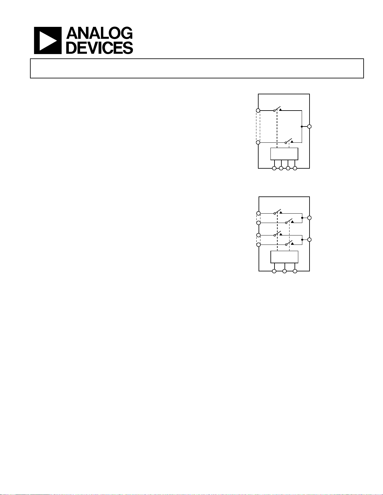
ADG1608/ADG1609
FUNCTIONAL BLOCK DIAGRAMS
ADG1608
S1
D
S8
1-OF-8
DECODER
A0 A1 A2 EN
Figure 1.
ADG1609
S1A
S4A
4B
1-OF-4
DECODER
DA
DB
08318-001
GENERAL DESCRIPTION
The ADG1608/ADG1609 are monolithic CMOS analog multiplexers comprising eight single channels and four differential
channels, respectively. The ADG1608 switches one of eight
inputs to a common output, as determined by the 3-bit binary
address lines, A0, A1, and A2. The ADG1609 switches one of
four differential inputs to a common differential output, as
determined by the 2-bit binary address lines, A0 and A1. An
EN input on both devices is used to enable or disable the device.
When disabled, all channels are switched off.
Each switch conducts equally well in both directions when on
and has an input signal range that extends to the supplies. In the
off condition, signal levels up to the supplies are blocked. All
switches exhibit break-before-make switching action. Inherent
in the design is low charge injection for minimum transients
when switching the digital inputs.
Rev. 0
Information furnished by Analog Devices is believed to be accurate and reliable. However, no
responsibility is assumed by Analog Devices for its use, nor for any infringements of patents or other
rights of third parties that may result from its use. Specifications subject to change without notice. No
license is granted by implication or otherwise under any patent or patent rights of Analog Devices.
Trademarks and registered trademarks are the property of their respective owners.
A0 A1 EN
Figure 2.
08318-002
The low on resistance of these switches make them ideal solutions for data acquisition and gain switching applications where
low on resistance and distortion is critical. The on-resistance
profile is very flat over the full analog input range, ensuring
excellent linearity and low distortion when switching audio
signals.
CMOS construction ensures ultralow power dissipation,
making the parts ideally suited for portable and batterypowered instruments.
PRODUCT HIGHLIGHTS
1. 8 Ω maximum on resistance over temperature.
2. Minimum distortion: THD + N = 0.04%
3. 3 V logic-compatible digital inputs: V
4. No V
logic power supply required.
L
5. Ultralow power dissipation: <8 nW.
6. 16-lead TSSOP and 16-lead, 3 mm × 3 mm LFCSP.
One Technology Way, P.O. Box 9106, Norwood, MA 02062-9106, U.S.A.
Tel: 781.329.4700 www.analog.com
Fax: 781.461.3113 ©2009 Analog Devices, Inc. All rights reserved.
= 2.0 V, V
INH
= 0.8 V.
INL

ADG1608/ADG1609
TABLE OF CONTENTS
Features .............................................................................................. 1
Applications ....................................................................................... 1
Functional Block Diagrams ............................................................. 1
General Description ......................................................................... 1
Product Highlights ........................................................................... 1
Revision History ............................................................................... 2
Specifications ..................................................................................... 3
±5 V Dual Supply ......................................................................... 3
12 V Single Supply ........................................................................ 4
5 V Single Supply .......................................................................... 4
3.3 V Single Supply ....................................................................... 6
REVISION HISTORY
7/09—Revision 0: Initial Version
Continuous Current per Channel, S or D ..................................7
Absolute Maximum Ratings ............................................................8
ESD Caution...................................................................................8
Pin Configurations and Function Descriptions ............................9
Typical Performance Characteristics ........................................... 11
Test Circuits ..................................................................................... 14
Terminolog y .................................................................................... 17
Outline Dimensions ....................................................................... 18
Ordering Guide .......................................................................... 18
Rev. 0 | Page 2 of 20

ADG1608/ADG1609
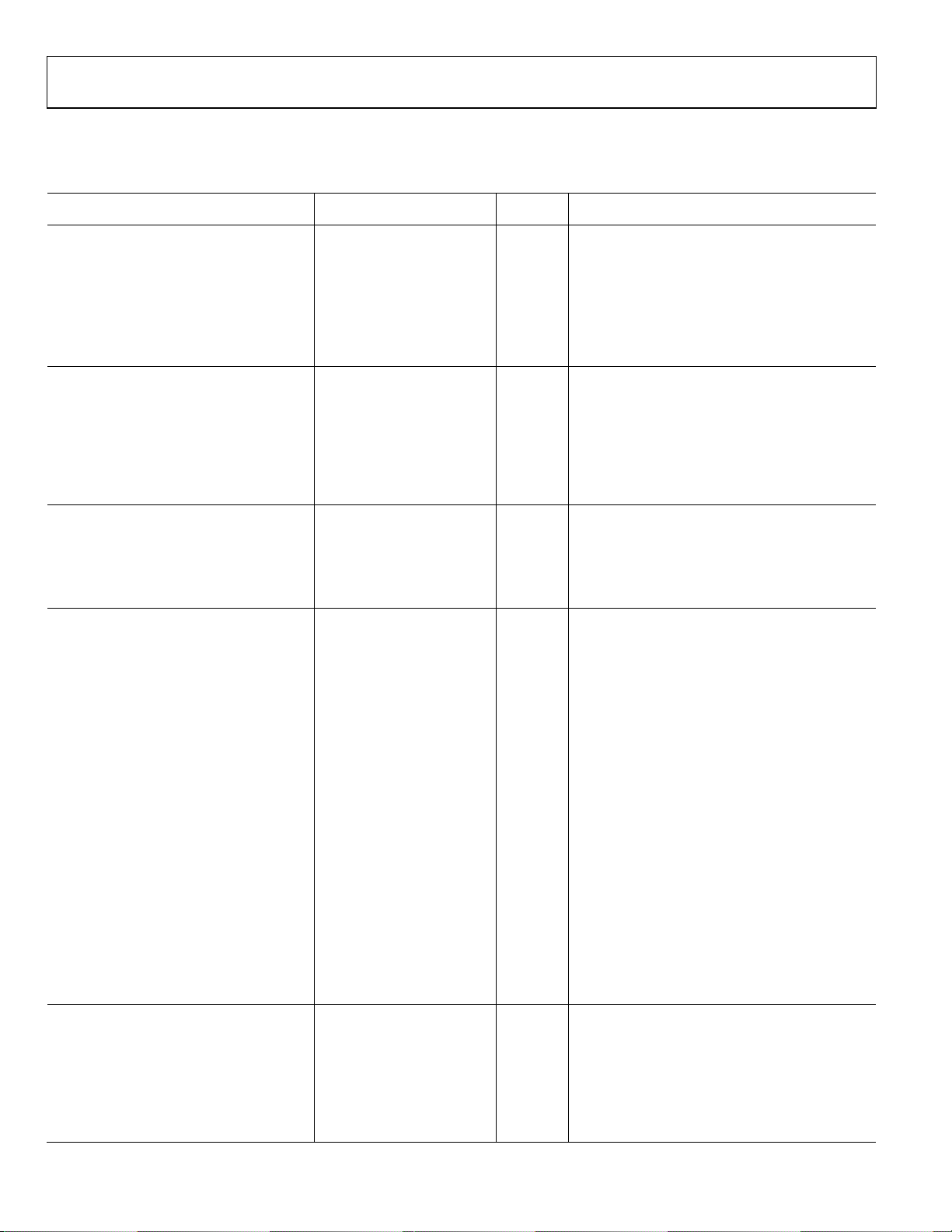
SPECIFICATIONS
±5 V DUAL SUPPLY
VDD = +5 V ± 10%, VSS = −5 V ± 10%, GND = 0 V, unless otherwise noted.
Table 1.
−40°C to
Parameter 25°C
+85°C
ANALOG SWITCH
Analog Signal Range VDD to VSS V
On Resistance (RON) 4.5 Ω typ VS = ±4.5 V, IS = −10 mA; see Figure 25
5 7 8 Ω max VDD = ±4.5 V, VSS = ±4.5 V
On-Resistance Match Between Channels (∆RON) 0.12 Ω typ VS = ±4.5 V, IS = −10 mA
0.25 0.3 0.35 Ω max
On-Resistance Flatness (R
) 1 Ω typ VS = ±4.5 V, IS = −10 mA
FLAT(ON)
1.3 1.7 2 Ω max
LEAKAGE CURRENTS VDD = +5.5 V, VSS = −5.5 V
Source Off Leakage, IS (Off) ±0.02 nA typ
±0.1 ±0.5 ±3 nA max
Drain Off Leakage, ID (Off) ±0.03 nA typ
ADG1608 ±0.15 ±2 ±14 nA max
ADG1609 ±0.15 ±1 ±7 nA max
Channel On Leakage, ID, IS (On) ±0.03 nA typ VS = VD = ±4.5 V; see Figure 27
±0.15 ±2 ±14 nA max
DIGITAL INPUTS
Input High Voltage, V
Input Low Voltage, V
Input Current, I
2.0 V min
INH
0.8 V max
INL
or I
±1 nA typ VIN = V
INL
INH
±0.1 μA max
Digital Input Capacitance, CIN 4 pF typ
DYNAMIC CHARACTERISTICS1
Transition Time, t
150 ns typ RL = 300 Ω, CL = 35 pF
TRANSITION
182 230 258 ns max VS = 2.5 V; see Figure 28
tON (EN) 106 ns typ RL = 300 Ω, CL = 35 pF
132 150 160 ns max VS = 2.5 V; see Figure 30
t
(EN) 113 ns typ RL = 300 Ω, CL = 35 pF
OFF
144 178 202 ns max VS = 2.5 V; see Figure 30
Break-Before-Make Time Delay, tD 47 ns typ RL = 300 Ω, CL = 35 pF
30 ns min VS1 = VS2 = 2.5 V; see Figure 29
Charge Injection 24 pC typ VS = 0 V, RS = 0 Ω, CL = 1 nF; see Figure 31
Off Isolation −64 dB typ RL = 50 Ω, CL = 5 pF, f = 1 MHz; see Figure 32
Channel-to-Channel Crosstalk −64 dB typ RL = 50 Ω, CL = 5 pF, f = 1 MHz; see Figure 34
Total Harmonic Distortion + Noise (THD + N) 0.04 % typ RL = 110 Ω, VS = 5 V p-p, f = 20 Hz to 20 kHz; see Figure 35
−3 dB Bandwidth RL = 50 Ω, CL = 5 pF; see Figure 33
ADG1608 40 MHz typ
ADG1609 71 MHz typ
CS (Off) 20 pF typ VS = 0 V, f = 1 MHz
CD (Off)
ADG1608 120 pF typ VS = 0 V, f = 1 MHz
ADG1609 61 pF typ VS = 0 V, f = 1 MHz
CD, CS (On)
ADG1608 153 pF typ VS = 0 V, f = 1 MHz
ADG1609 85 pF typ VS = 0 V, f = 1 MHz
POWER REQUIREMENTS VDD = +5.5 V, VSS = −5.5 V
IDD 0.001 μA typ Digital inputs = 0 V or VDD
1.0 μA max
VDD/VSS ±3.3/±8 V min/max
1
Guaranteed by design, but not subject to production test.
−40°C to
+125°C
Unit Test Conditions/Comments
V
= ±4.5 V, VD = ∓4.5 V; see Figure 26
S
V
= ±4.5 V, VD = ∓4.5 V; see Figure 26
S
or VDD
GND
Rev. 0 | Page 3 of 20
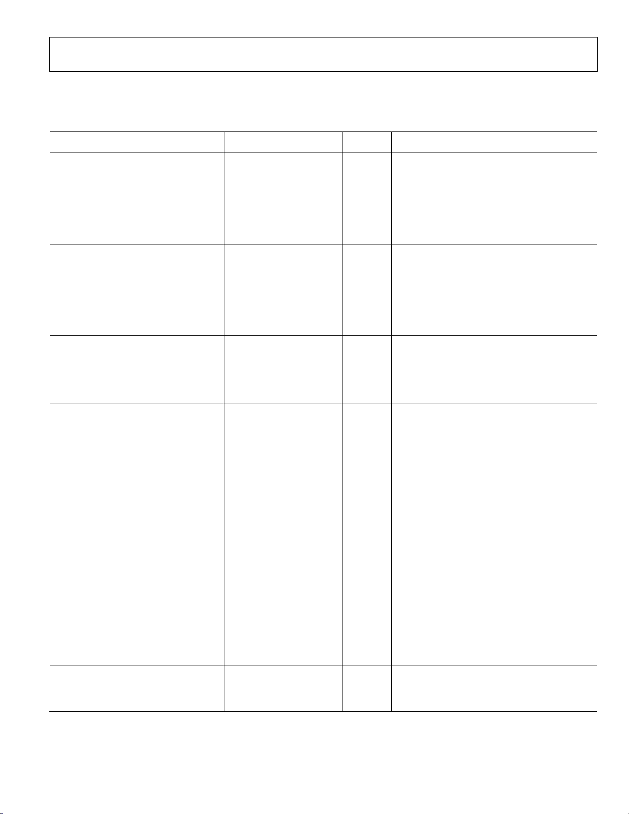
ADG1608/ADG1609
12 V SINGLE SUPPLY
VDD = 12 V ± 10%, VSS = 0 V, GND = 0 V, unless otherwise noted.
Table 2.
Parameter 25°C
+85°C
ANALOG SWITCH
Analog Signal Range 0 V to VDD V
On Resistance (RON) 4 Ω typ VS = 0 V to 10 V, IS = −10 mA; see Figure 25
4.5 6.5 7.5 Ω max VDD = 10.8 V, VSS = 0 V
On-Resistance Match Between Channels (∆RON) 0.12 Ω typ VS = 10 V, IS = −10 mA
0.25 0.3 0.35 Ω max
−40°C to
On-Resistance Flatness (R
) 0.9 Ω typ VS = 0 V to 10 V, IS = −10 mA
FLAT(ON)
1.2 1.6 1.9 Ω max
LEAKAGE CURRENTS VDD = 13.2 V, VSS = 0 V
Source Off Leakage, IS (Off) ±0.02 nA typ VS = 1 V/10 V, VD = 10 V/1 V; see Figure 26
±0.1 ±0.5 ±3 nA max
Drain Off Leakage, ID (Off) ±0.03 nA typ VS = 1 V/10 V, VD = 10 V/1 V; see Figure 26
ADG1608 ±0.15 ±2 ±14 nA max
ADG1609 ±0.15 ±1 ±7 nA max
Channel On Leakage, ID, IS (On) ±0.03 nA typ VS = VD = 1 V or 10 V; see Figure 27
±0.15 ±2 ±14 nA max
DIGITAL INPUTS
Input High Voltage, V
Input Low Voltage, V
Input Current, I
2.0 V min
INH
0.8 V max
INL
or I
±1 nA typ VIN = V
INL
INH
±0.1 μA max
Digital Input Capacitance, CIN 4 pF typ
DYNAMIC CHARACTERISTICS1
Transition Time, t
113 ns typ RL = 300 Ω, CL = 35 pF
TRANSITION
141 172 196 ns max VS = 8 V; see Figure 28
tON (EN) 80 ns typ RL = 300 Ω, CL = 35 pF
94 101 110 ns max VS = 8 V; see Figure 30
t
(EN) 77 ns typ RL = 300 Ω, CL = 35 pF
OFF
93 117 140 ns max VS = 8 V; see Figure 30
Break-Before-Make Time Delay, tD 47 ns typ RL = 300 Ω, CL = 35 pF
30 ns min VS1 = VS2 = 8 V; see Figure 29
Charge Injection 29 pC typ VS = 6 V, RS = 0 Ω, CL = 1 nF; see Figure 31
Off Isolation −64 dB typ RL = 50 Ω, CL = 5 pF, f = 1 MHz; see Figure 32
Channel-to-Channel Crosstalk −64 dB typ RL = 50 Ω, CL = 5 pF, f = 1 MHz; see Figure 34
Total Harmonic Distortion + Noise (THD + N) 0.04 % typ RL = 110 Ω, VS = 5 V p-p, f = 20 Hz to 20 kHz; see Figure 35
−3 dB Bandwidth RL = 50 Ω, CL = 5 pF; see Figure 33
ADG1608 40 MHz typ
ADG1609 78 MHz typ
CS (Off) 19 pF typ VS = 6 V, f = 1 MHz
CD (Off)
ADG1608 117 pF typ VS = 6 V, f = 1 MHz
ADG1609 59 pF typ VS = 6 V, f = 1 MHz
CD, CS (On)
ADG1608 149 pF typ VS = 6 V, f = 1 MHz
ADG1609 84 pF typ VS = 6 V, f = 1 MHz
POWER REQUIREMENTS VDD = 12 V
IDD 0.001 μA typ Digital inputs = 0 V or VDD
1.0 μA max
ADG1608 300 μA typ Digital inputs = 5 V
480 μA max
ADG1609 225 μA typ Digital inputs = 5 V
360 μA max
VDD 3.3/16 V min/max
1
Guaranteed by design, but not subject to production test.
−40°C to
+125°C Unit Test Conditions/Comments
or VDD
GND
Rev. 0 | Page 4 of 20
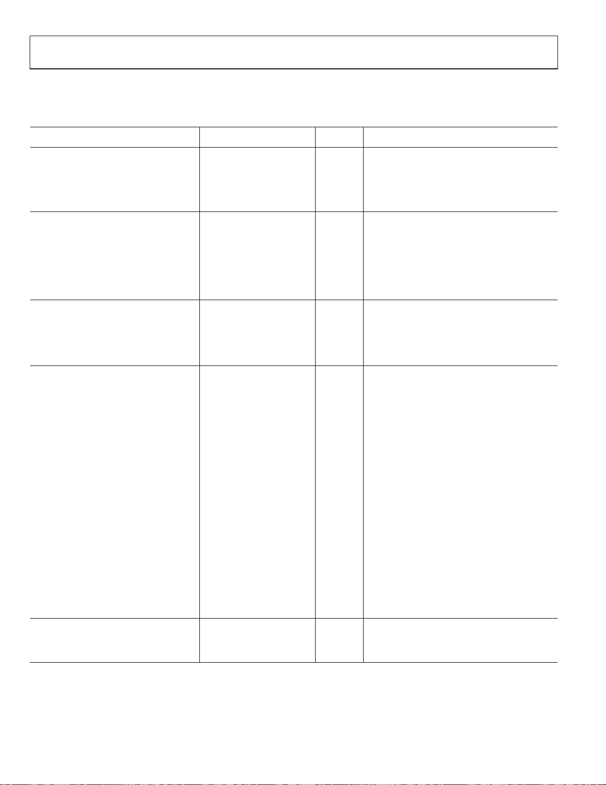
ADG1608/ADG1609
5 V SINGLE SUPPLY
VDD = 5 V ± 10%, VSS = 0 V, GND = 0 V, unless otherwise noted.
Table 3.
−40°Cto
Parameter 25°C
+85°C
ANALOG SWITCH
Analog Signal Range 0 V to VDD V
On Resistance (RON) 8.5 Ω typ VS = 0 V to 4.5 V, IS = −10 mA; see Figure 25
10 12.5 14 Ω max VDD = 4.5 V, VSS = 0 V
On-Resistance Match Between Channels (∆RON) 0.15 Ω typ VS = 0 V to 4.5 V, IS = −10 mA
0.3 0.35 0.4 Ω max
On-Resistance Flatness (R
) 1.7 Ω typ VS = 0 V to 4.5 V, IS = −10 mA
FLAT(ON)
2.3 2.7 3 Ω max
LEAKAGE CURRENTS VDD = 5.5 V, VSS = 0 V
Source Off Leakage, IS (Off) ±0.01 nA typ VS = 1 V/4.5 V, VD = 4.5 V/1 V; see Figure 26
±0.1 ±0.5 ±3 nA max
Drain Off Leakage, ID (Off) ±0.01 nA typ VS = 1 V/4.5 V, VD = 4.5 V/1 V; see Figure 26
ADG1608 ±0.15 ±2 ±14 nA max
ADG1609 ±0.15 ±1 ±7 nA max
Channel On Leakage, ID, IS (On) ±0.01 nA typ VS = VD = 1 V or 4.5 V; see Figure 27
±0.15 ±2 ±14 nA max
DIGITAL INPUTS
Input High Voltage, V
Input Low Voltage, V
Input Current, I
2.0 V min
INH
0.8 V max
INL
or I
±1 nA typ VIN = V
INL
INH
±0.1 μA max
Digital Input Capacitance, CIN 4 pF typ
DYNAMIC CHARACTERISTICS1
Transition Time, t
193 ns typ RL = 300 Ω, CL = 35 pF
TRANSITION
251 301 339 ns max VS = 2.5 V; see Figure 28
tON (EN) 115 ns typ RL = 300 Ω, CL = 35 pF
152 171 184 ns max VS = 2.5 V; see Figure 30
t
(EN) 140 ns typ RL = 300 Ω, CL = 35 pF
OFF
184 225 259 ns max VS = 2.5 V; see Figure 30
Break-Before-Make Time Delay, tD 66 ns typ RL = 300 Ω, CL = 35 pF
37 ns min VS1 = VS2 = 2.5 V; see Figure 29
Charge Injection 11 pC typ VS = 2.5 V, RS = 0 Ω, CL = 1 nF; see Figure 31
Off Isolation −64 dB typ RL = 50 Ω, CL = 5 pF, f = 100 kHz; see Figure 32
Channel-to-Channel Crosstalk −64 dB typ RL = 50 Ω, CL = 5 pF, f = 100 kHz; see Figure 34
Total Harmonic Distortion + Noise (THD + N) 0.3 % typ RL = 110 Ω, f = 20 Hz to 20 kHz, VS = 3.5 V p-p; se e Figure 35
−3 dB Bandwidth RL = 50 Ω, CL = 5 pF; see Figure 33
ADG1608 37 MHz typ
ADG1609 72 MHz typ
CS (Off) 22 pF typ VS = 2.5 V, f = 1 MHz
CD (Off) VS = 2.5 V, f = 1 MHz
ADG1608 136 pF typ
ADG1609 68 pF typ
CD, CS (On) VS = 2.5 V, f = 1 MHz
ADG1608 168 pF typ
ADG1609 94 pF typ
POWER REQUIREMENTS VDD = 5.5 V
IDD 0.001 μA typ Digital inputs = 0 V or VDD
1.0 μA max
VDD 3.3/16 V min/max
1
Guaranteed by design, but not subject to production test.
−40°C to
+125°C
Unit Test Conditions/Comments
or VDD
GND
Rev. 0 | Page 5 of 20
ADG1608/ADG1609
3.3 V SINGLE SUPPLY
VDD = 3.3 V, VSS = 0 V, GND = 0 V, unless otherwise noted.
Table 4.
−40°C to
Parameter 25°C
+85°C
ANALOG SWITCH
Analog Signal Range 0 V to VDD V
On Resistance (RON) 13.5 15 16.5 Ω typ VS = 0 V to VDD, IS = −10 mA; see Figure 25, VDD = 3.3 V,
On-Resistance Match Between Channels (∆RON) 0.25 0.28 0.3 Ω typ VS = 0 V to VDD, IS = −10 mA
On-Resistance Flatness (R
) 5 5.5 6.5 Ω typ VS = 0 V to VDD, IS = −10 mA
FLAT(ON)
LEAKAGE CURRENTS VDD = 3.6 V, VSS = 0 V
Source Off Leakage, IS (Off) ±0.01 nA typ VS = 0.6 V/3 V, VD = 3 V/0.6 V; see Figure 26
±0.1 ±0.5 ±3 nA max
Drain Off Leakage, ID (Off) ±0.01 nA typ VS = 0.6 V/3 V, VD = 3 V/0.6 V; see Figure 26
ADG1608 ±0.15 ±2 ±14 nA max
ADG1609 ±0.15 ±1 ±7 nA max
Channel On Leakage, ID, IS (On) ±0.01 nA typ VS = VD = 0.6 V or 3 V; see Figure 27
±0.15 ±2 ±14 nA max
DIGITAL INPUTS
Input High Voltage, V
Input Low Voltage, V
Input Current, I
2.0 V min
INH
0.8 V max
INL
or I
±1 nA typ VIN = V
INL
INH
±0.1 μA max
Digital Input Capacitance, CIN 4 pF typ
DYNAMIC CHARACTERISTICS1
Transition Time, t
312 ns typ RL = 300 Ω, CL = 35 pF
TRANSITION
437 498 542 ns max VS = 1.5 V; see Figure 28
tON (EN) 216 ns typ RL = 300 Ω, CL = 35 pF
309 331 344 ns max VS = 1.5 V; see Figure 30
t
(EN) 236 ns typ RL = 300 Ω, CL = 35 pF
OFF
316 367 411 ns max VS = 1.5 V; see Figure 30
Break-Before-Make Time Delay, tD 104 ns typ RL = 300 Ω, CL = 35 pF
48 ns min VS1 = VS2 = 1.5 V; see Figure 29
Charge Injection 6 pC typ VS = 1.5 V, RS = 0 Ω, CL = 1 nF; see Figure 31
Off Isolation −64 dB typ RL = 50 Ω, CL = 5 pF, f = 100 kHz; see Figure 32
Channel-to-Channel Crosstalk −64 dB typ RL = 50 Ω, CL = 5 pF, f = 100 kHz; see Figure 34
Total Harmonic Distortion + Noise (THD + N) 0.5 % typ RL = 110 Ω, f = 20 Hz to 20 kHz, VS = 2 V p-p; see Figure 35
−3 dB Bandwidth RL = 50 Ω, CL = 5 pF; see Figure 33
ADG1608 34 MHz typ
ADG1609 72 MHz typ
CS (Off) 23 pF typ VS = 1.5 V, f = 1 MHz
CD (Off) VS = 1.5 V, f = 1 MHz
ADG1608 145 pF typ
ADG1609 72 pF typ
CD, CS (On) VS = 1.5 V, f = 1 MHz
ADG1608 173 pF typ
ADG1609 95 pF typ
POWER REQUIREMENTS VDD = 3.6 V
IDD 0.001 μA typ Digital inputs = 0 V or VDD
1.0 μA max
VDD 3.3/16 V min/max
1
Guaranteed by design, but not subject to production test.
−40°C to
+125°C
Unit Test Conditions/Comments
= 0 V
V
SS
or VDD
GND
Rev. 0 | Page 6 of 20

ADG1608/ADG1609
CONTINUOUS CURRENT PER CHANNEL, S OR D
Table 5. ADG1608
Parameter 25°C 85°C 125°C Unit
CONTINUOUS CURRENT, S OR D
VDD = +5 V, VSS = −5 V
TSSOP (θJA = 112.6°C/W) 290 180 100 mA max
LFCSP (θJA = 48.7°C/W) 470 255 120 mA max
VDD = 12 V, VSS = 0 V
TSSOP (θJA = 112.6°C/W) 213 129 73 mA max
LFCSP (θJA = 48.7°C/W) 346 185 84 mA max
VDD = 5 V, VSS = 0 V
TSSOP (θJA = 112.6°C/W) 157 101 63 mA max
LFCSP (θJA = 48.7°C/W) 252 150 77 mA max
VDD = 3.3 V, VSS = 0 V
TSSOP (θJA = 112.6°C/W) 126 87 56 mA max
LFCSP (θJA = 48.7°C/W) 206 129 73.5 mA max
Table 6. ADG1609
Parameter 25°C 85°C 125°C Unit
CONTINUOUS CURRENT, S OR D
VDD = +5 V, VSS = −5 V
TSSOP (θJA = 112.6°C/W) 147 98 63 mA max
LFCSP (θJA = 48.7°C/W) 245 147 77 mA max
VDD = 12 V, VSS = 0 V
TSSOP (θJA = 112.6°C/W) 157 101 63 mA max
LFCSP (θJA = 48.7°C/W) 255 150 77 mA max
VDD = 5 V, VSS = 0 V
TSSOP (θJA = 112.6°C/W) 115 80 52 mA max
LFCSP (θJA = 48.7°C/W) 189 119 70 mA max
VDD = 3.3 V, VSS = 0 V
TSSOP (θJA = 112.6°C/W) 94 66 45 mA max
LFCSP (θJA = 48.7°C/W) 154 101 63 mA max
Rev. 0 | Page 7 of 20

ADG1608/ADG1609
ABSOLUTE MAXIMUM RATINGS
TA = 25°C, unless otherwise noted.
Table 7.
Parameter Rating
VDD to VSS 18 V
VDD to GND −0.3 V to +18 V
VSS to GND +0.3 V to −18 V
Analog Inputs1
Digital Inputs1
Peak Current, S or D
Continuous Current, S or D2 Data + 15%
Operating Temperature Range
Industrial (Y Version) −40°C to +125°C
Storage Temperature Range −65°C to +150°C
Junction Temperature 150°C
16-Lead TSSOP, θJA Thermal
Impedance, 0 Airflow
(4-Layer Board)
16-Lead LFCSP, θJA Thermal
Impedance, 0 Airflow
(4-Layer Board)
Reflow Soldering Peak
Temperature, Pb free
1
Overvoltages at IN, S, or D are clamped by internal diodes. Current should be
limited to the maximum ratings given.
2
See Table 5 and Table 6.
− 0.3 V to VDD + 0.3 V or
V
SS
30 mA, whichever occurs first
GND − 0.3 V to V
30 mA, whichever occurs first
710 mA (pulsed at 1 ms,
10% duty cycle maximum)
112.6°C/W
48.7°C/W
260°C
+ 0.3 V or
DD
Stresses above those listed under Absolute Maximum Ratings
may cause permanent damage to the device. This is a stress
rating only; functional operation of the device at these or any
other conditions above those indicated in the operational
section of this specification is not implied. Exposure to absolute
maximum rating conditions for extended periods may affect
device reliability.
ESD CAUTION
Rev. 0 | Page 8 of 20

ADG1608/ADG1609
V
V
PIN CONFIGURATIONS AND FUNCTION DESCRIPTIONS
A0
EN
A2
A1
14
13
15
16
PIN 1
INDICATOR
1
SS
2S1
ADG1608
3S2
A0
EN
V
SS
S1
S2
S3
S4
D
1
2
3
ADG1608
4
TOP VIEW
5
(Not to Scale)
6
7
8
16
A1
15
A2
14
GND
13
V
DD
12
S5
11
S6
10
S7
9
S8
8318-003
Figure 3. ADG1608 Pin Configuration (TSSOP)
NOTES
1. THE EXPOSED PAD IS CONNECTED
INTERNALLY. FOR INCREASED
RELIABILITY OF THE SOLDER
JOINTS AND MAXIMUM THERMAL
CAPABILITY, IT IS RECOMMENDED
THAT THE PAD BE SOLDERED TO
THE SUBSTRATE,
Figure 4. ADG1608 Pin Configuration (LFCSP)
4S3
TOP VIEW
(Not to Scale)
5
6
D
S4
Table 8. ADG1608 Pin Function Descriptions
Pin No.
TSSOP LFCSP Mnemonic Description
1 15 A0 Logic Control Input.
2 16 EN
Active High Digital Input. When this pin is low, the device is disabled and all switches are off. When this pin
is high, Ax logic inputs determine on switches.
3 1 VSS Most Negative Power Supply Potential. In single-supply applications, this pin can be connected to ground.
4 2 S1 Source Terminal 1. Can be an input or an output.
5 3 S2 Source Terminal 2. Can be an input or an output.
6 4 S3 Source Terminal 3. Can be an input or an output.
7 5 S4 Source Terminal 4. Can be an input or an output.
8 6 D Drain Terminal. Can be an input or an output.
9 7 S8 Source Terminal 8. Can be an input or an output.
10 8 S7 Source Terminal 7. Can be an input or an output.
11 9 S6 Source Terminal 6. Can be an input or an output.
12 10 S5 Source Terminal 5. Can be an input or an output.
13 11 VDD Most Positive Power Supply Potential.
14 12 GND Ground (0 V) Reference.
15 13 A2 Logic Control Input.
16 14 A1 Logic Control Input.
N/A EP EP
Exposed Pad. The exposed pad is connected internally. For increased reliability of the solder joints and
maximum thermal capability, it is recommended that the pad be soldered to the substrate, V
12 GND
11 V
DD
10 S5
9S6
8
7
S8
S7
.
SS
08318-004
.
SS
Table 9. ADG1608 Truth Table
A2 A1 A0 EN On Switch
X1 X
1
X
1
0 None
0 0 0 1 1
0 0 1 1 2
0 1 0 1 3
0 1 1 1 4
1 0 0 1 5
1 0 1 1 6
1 1 0 1 7
1 1 1 1 8
1
X = don’t care.
Rev. 0 | Page 9 of 20

ADG1608/ADG1609
A0
EN
A1
GND
14
13
15
16
PIN 1
INDICATOR
1V
SS
2S1A
ADG1609
3S2A
A0
EN
V
S1A
S2A
S3A
S4A
DA
SS
1
2
3
ADG1609
4
TOP VIEW
5
(Not to Scale)
6
7
8
16
A1
15
GND
14
V
DD
13
S1B
12
S2B
11
S3B
10
S4B
9
DB
8318-005
Figure 5. ADG1609 Pin Configuration (TSSOP)
NOTES
1. THE EXPOSED PAD IS CONNECTED
INTERNALLY. FOR INCREASED
RELIABILITY OF THE SOLDER
JOINTS AND MAXIMUM THERMAL
CAPABILITY, IT IS RECOMMENDED
THAT THE PAD BE SOLDERED TO
THE SUBSTRATE, V
Figure 6. ADG1609 Pin Configuration (LFCSP)
4S3A
TOP VIEW
(Not to Scal e)
5
6
DA
S4A
Table 10. ADG1609 Pin Function Descriptions
Pin No.
TSSOP LFCSP Mnemonic Description
1 15 A0 Logic Control Input.
2 16 EN
Active High Digital Input. When this pin is low, the device is disabled and all switches are off. When this pin
is high, Ax logic inputs determine on switches.
3 1 VSS Most Negative Power Supply Potential. In single-supply applications, this pin can be connected to ground.
4 2 S1A Source Terminal 1A. Can be an input or an output.
5 3 S2A Source Terminal 2A. Can be an input or an output.
6 4 S3A Source Terminal 3A. Can be an input or an output.
7 5 S4A Source Terminal 4A. Can be an input or an output.
8 6 DA Drain Terminal A. Can be an input or an output.
9 7 DB Drain Terminal B. Can be an input or an output.
10 8 S4B Source Terminal 4B. Can be an input or an output.
11 9 S3B Source Terminal 3B. Can be an input or an output.
12 10 S2B Source Terminal 2B. Can be an input or an output.
13 11 S1B Source Terminal 1B. Can be an input or an output.
14 12 VDD Most Positive Power Supply Potential.
15 13 GND Ground (0 V) Reference.
16 14 A1 Logic Control Input.
N/A EP EP
Exposed Pad. The exposed pad is connected internally. For increased reliability of the solder joints and
maximum thermal capability, it is recommended that the pad be soldered to the substrate, V
12 V
DD
11 S1B
10 S2B
9S3B
8
7
SB
S4B
.
SS
08318-006
.
SS
Table 11. ADG1609 Truth Table
A1 A0 EN On Switch Pair
X1 X
1
0 None
0 0 1 1
0 1 1 2
1 0 1 3
1 1 1 4
1
X = don’t care.
Rev. 0 | Page 10 of 20

ADG1608/ADG1609
TYPICAL PERFORMANCE CHARACTERISTICS
7
6
TA = 25°C
7
6
VDD = 12V
V
= 0V
SS
5
= +3.3V
V
DD
V
= –3.3V
4
3
ON RESISTANCE ()
2
1
0
–8 –6 –4 –2 0 2 4 6 8
SOURCE OR DRAIN VO LTAGE (V)
SS
V
= +5V
DD
V
= –5V
SS
VDD = +8V
V
= –8V
SS
Figure 7. On Resistance vs. VD (VS) for Dual Supply
16
14
12
10
8
6
ON RESISTANCE ()
4
2
0
0
VDD = 3.3V
V
= 0V
SS
VDD = 5V
V
= 0V
SS
VDD = 12V
V
SS
2
6
4
SOURCE OR DRAIN VO LTAGE (V)
= 0V
810
12 14 16
Figure 8. On Resistance vs. VD (VS) for Single Supply
TA = 25°C
VDD = 16V
V
= 0V
SS
5
4
3
ON RESISTANCE ()
2
1
0
024681012
08318-029
SOURCE OR DRAIN VO LTAGE (V)
TA = +125°C
TA = +85°C
TA = +25°C
TA = –40°C
8318-032
Figure 10. On Resistance vs. VD (VS) for Different Temperatures,
12 V Single Supply
12
10
8
6
4
ON RESISTANCE ()
2
0
0 0.5 1.0 1.5 2.0 2.5 3.0 3.5 4.0 4.5 5.0
08318-030
SOURCE OR DRAIN VO LTAGE (V)
TA = +125°C
TA = +85°C
TA = +25°C
TA = –40°C
VDD = 5V
V
= 0V
SS
08318-033
Figure 11. On Resistance vs. VD (VS) for Different Temperatures,
5 V Single Supply
7
6
5
4
3
ON RESISTANCE ()
2
1
0
–5 –4 –3 –2 –1 0 1 2 3 4 5
SOURCE OR DRAIN VO LTAGE (V)
TA = +125°C
TA = +85°C
TA = +25°C
TA = –40°C
VDD = +5V
V
= –5V
SS
Figure 9. On Resistance vs. VD (VS) for Different Temperatures,
±5 V Dual Supply
8318-031
Rev. 0 | Page 11 of 20
18
VDD = 3.3V
V
= 0V
SS
16
14
12
10
8
6
ON RESISTANCE ()
4
2
0
0 0.5 1.0 1.5 2.0 2.5 3.0
SOURCE OR DRAIN VO LTAGE (V)
TA = +125°C
T
= +85°C
A
T
= +25°C
A
T
= –40°C
A
Figure 12. On Resistance vs. VD (VS) for Different Temperatures,
3.3 V Single Supply
08318-020

ADG1608/ADG1609
12
VDD = +5V
V
= –5V
SS
10
V
= +4.5V/–4.5V
BIAS
8
6
4
ID (OFF) – +
I
, IS (ON) + +
D
I
(OFF) + –
S
2
0
–2
LEAKAGE CURRENT (n A)
–4
–6
–8
0
20 40 60 80 100 120
, IS (ON) – –
I
D
I
(OFF) – +
S
I
(OFF) + –
D
TEMPERATURE (°C)
Figure 13. ADG1608 Leakage Currents vs. Temperature,
±5 V Dual Supply
8318-035
9
VDD = 3.3V
V
= 0V
SS
8
V
= 0.6V/3V
BIAS
7
6
5
4
3
2
LEAKAGE CURRENT ( nA)
1
ID, IS (ON) + +
I
(OFF) – +
D
I
, IS (ON) – –
D
I
(OFF) + –
S
I
(OFF) + –
D
I
(OFF) – +
S
0
–1
0 20406080100120
TEMPERATURE (°C)
Figure 16. ADG1608 Leakage Currents vs. Temperature,
3.3 V Single Supply
08318-018
15
VDD = 12V
= 0V
V
SS
= 1V/10V
V
BIAS
10
ID, IS (ON) + +
(OFF) – +
I
D
(OFF) + –
I
5
S
0
LEAKAGE CURRENT (n A)
–5
–10
0 20406080100120
, IS (ON) – –
I
D
(OFF) – +
I
S
(OFF) + –
I
D
TEMPERATURE (°C)
Figure 14. ADG1608 Leakage Currents vs. Temperature,
12 V Single Supply
10
VDD = 5V
= 0V
V
9
SS
= 1V/4.5V
V
BIAS
8
7
6
5
4
3
2
LEAKAGE CURRENT (nA)
ID, IS (ON) + +
(OFF) – +
I
D
, IS (ON) – –
I
D
(OFF) + –
I
S
(OFF) – +
I
S
(OFF) + –
I
D
1
0
–1
0 20 40 60 80 100 120
TEMPERATURE (°C)
Figure 15.ADG1608 Leakage Currents vs. Temperature,
5 V Single Supply
600
500
IDD = +12V
I
= 0V
SS
IDD PER CHANNEL
T
= 25°C
A
400
300
(µA)
DD
I
200
100
0
02468101214
08318-034
IDD = +5V
I
= –5V
SS
IDD = +5V
I
= 0V
SS
= +3.3V
I
DD
I
= 0V
SS
LOGIC (V)
08318-019
Figure 17. IDD vs. Logic Level
30
25
20
VDD= +5V
= –5V
V
SS
V
= +12V
DD
VSS= 0V
15
10
CHARGE INJECTI ON (pC)
5
0
–6 –4 –2 0 2 4 6 8 10 12 14
08318-036
Figure 18. Charge Injection vs. Source Voltage
V
V
VS (V)
DD
SS
V
V
= +3.3V
= 0V
= +5V
DD
= 0V
SS
08318-026
Rev. 0 | Page 12 of 20

ADG1608/ADG1609
A
450
400
350
VDD= +3.3V, VSS= 0V
300
250
200
V
= +5V, VSS= 0V
DD
150
TRANSITION TIME (ns)
100
50
0
–40 –20 0 20 40 60 80 100 120
= +12V, VSS= 0V
V
DD
= +5V, VSS= –5V
V
DD
TEMPERATURE (°C)
Figure 19. Transition Time vs. Temperature
TA = 25°C
8318-024
0
–1
–2
–3
–4
INSERTIO N LOSS (d B)
–5
TA = 25°C
V
= +5V
DD
V
= –5V
SS
–6
10k 100k 1M 10M 100M
FREQUENCY ( Hz)
Figure 22. On Response vs. Frequency
8318-021
0
T
= 25°C
A
V
= +5V
DD
–10
V
= –5V
SS
–20
–30
–40
TION (dB)
–50
–60
OFF ISOL
–70
–80
–90
–100
10k 100k 1M 10M 100M 1G
FREQUENCY ( Hz)
Figure 20. Off Isolation vs. Frequency
0
T
= 25°C
A
V
= +5V
DD
–10
V
= –5V
SS
–20
–30
–40
–50
–60
CROSSTALK (dB)
–70
–80
–90
–100
10k 100k 1M 10M 100M 1G
FREQUENCY (Hz)
Figure 21. Crosstalk vs. Frequency
0
TA = 25°C
VDD= +5V
–20
VSS= –5V
–40
–60
ACPSRR (dB)
–80
–100
–120
1k 1M 10M 100M10k 10 0k
08318-023
NO DECOUPLING
CAPACITORS
FREQUENCY (Hz)
DECOUPLING
CAPACITORS
08318-027
Figure 23. ACPSRR vs. Frequency
0.6
LOAD = 110
T
= 25°C
A
0.5
VDD= +3.3V, VS= 2V p-p
0.4
0.3
V
= +5V, VS= 3.5V p-p
0.2
0.1
DD
= +5V, VSS= –5V, VS= 5V p-p
V
DD
0
V
DD
5k0 10k
FREQUENCY (Hz)
= +12V, VS= 5V p-p
15k 20k
08318-028
THD + N (%)
08318-022
Figure 24. THD + N vs. Frequency
Rev. 0 | Page 13 of 20

ADG1608/ADG1609
V
V
VDDV
VDDV
A
TEST CIRCUITS
V
IS(OFF) ID (OFF)
SD
I
S
DS
08318-007
S
Figure 25. On Resistance
SD
NC
NC = NO CONNECT
Figure 27. On Leakage
ID(ON)
A
V
D
08318-009
3V
ADDRESS
DRIVE (V
0V
t
TRANSITION
OUTPUT
)
IN
50% 50%
90%
t
< 20ns
r
t
< 20ns
f
t
TRANSITI ON
90%
V
A0
V
IN
50
A1
A2
ADG1608*
2.4V EN
SD
A A
Figure 26. Off Leakage
SS
DDVSS
S1
S2 TO S7
S8
GND
D
V
V
OUTPUT
100
V
D
08318-008
S1
S8
35pF
*SIMILAR CO NNECTION F OR ADG1609.
Figure 28. Address to Output Switching Times, t
TRANSITION
08318-010
SS
DDRESS
DRIVE (V
OUTPUT
3V
)
IN
0V
80% 80%
t
BBM
Figure 29. Break-Before-Make Delay, t
V
IN
50
2.4V EN
*SIMILAR CO NNECTION F OR ADG1609.
BBM
V
DD
A0
A1
A2
ADG1608*
GND
V
SS
S2 TO S7
S1
S8
D
OUTPUT
100
V
S
35pF
08318-011
Rev. 0 | Page 14 of 20

ADG1608/ADG1609
VDDV
VINV
VDDV
SS
3V
ENABLE
DRIVE (V
0V
OUTPUT
)
IN
t
(EN)
ON
3V
50% 50%
0.9V
O
t
(EN)
OFF
0.9V
O
Figure 30. Enable Delay, t
V
IN
50
*SIMILAR CO NNECTION F OR ADG1609.
(EN), t
OFF
(EN)
ON
V
DD
A0
A1
A2
ADG1608*
EN
V
DDVSS
A0
A1
A2
GND
V
SS
S2 TO S8
SS
S1
D
OUTPUT
100
V
S
35pF
08318-012
ADG1608*
R
OUT
Q
INJ
= CL × V
OUT
V
OUT
S
V
S
EN
V
IN
GND
DS
C
1nF
V
OUT
L
Figure 31. Charge Injection
*SIMILAR CONNECTION FOR ADG1609.
08318-013
Rev. 0 | Page 15 of 20

ADG1608/ADG1609
V
V
V
V
V
0.1µF
0.1µF
V
DD
V
SS
0.1µF
V
DD
SS
S
50
D
GND
OFF ISOLATION = 20 log
NETWORK
ANALYZER
50
V
OUT
R
L
50
V
S
V
OUT
V
08318-014
S
Figure 32. Off Isolation
NETWO RK
ANALYZER
V
OUT
R
L
50
V
S
CHANNEL-TO-CHANNEL CROSSTALK = 20 log
Figure 34. Channel-to-Channel Crosstalk
V
DD
V
SS
0.1µF
NETWORK
V
DD
SS
S
D
GND
ANALYZER
50
V
OUT
R
L
50
V
S
0.1µF
IN
V
IN
V
DD
V
SS
0.1µF
V
DD
SS
S
D
GND
0.1µF
DD
V
S1
S2
R
L
10k
V
DD
GND
V
OUT
V
S
AUDIO PRECISIO N
V
OUT
SS
0.1µF
SS
D
R
50
08318-015
R
S
V
S
V p-p
08318-017
INSERTION LOSS = 20 log
Figure 33. Bandwidth
WITH SWITCH
V
OUT
WITHOUT SWITCH
V
OUT
08318-016
Figure 35. THD + Noise
Rev. 0 | Page 16 of 20

ADG1608/ADG1609
TERMINOLOGY
IDD
The positive supply current.
I
SS
The negative supply current.
V
(VS)
D
The analog voltage on Terminal D and Terminal S.
R
ON
The ohmic resistance between Terminal D and Terminal S.
R
FLAT(ON)
Flatness that is defined as the difference between the maximum
and minimum value of on resistance measured over the specified
analog signal range.
I
(Off)
S
The source leakage current with the switch off.
I
(Off)
D
The drain leakage current with the switch off.
I
, IS (On)
D
The channel leakage current with the switch on.
V
INL
The maximum input voltage for Logic 0.
V
INH
The minimum input voltage for Logic 1.
I
(I
)
INL
INH
The input current of the digital input.
C
(Off)
S
The off switch source capacitance, which is measured with
reference to ground.
C
(Off)
D
The off switch drain capacitance, which is measured with
reference to ground.
C
, CS (On)
D
The on switch capacitance, which is measured with reference to
ground.
C
IN
The digital input capacitance.
t
TRANSITION
The delay time between the 50% and 90% points of the digital
input and switch on condition when switching from one address
state to another.
t
(EN)
ON
The delay between applying the digital control input and the
output switching on.
t
(EN)
OFF
The delay between applying the digital control input and the
output switching off .
Charge Injection
A measure of the glitch impulse transferred from the digital
input to the analog output during switching.
Off Isolation
A measure of unwanted signal coupling through an off switch.
Crosstalk
A measure of unwanted signal that is coupled through from one
channel to another as a result of parasitic capacitance.
Bandwidth
The frequency at which the output is attenuated by 3 dB.
On Response
The frequency response of the on switch.
Insertion Loss
The loss due to the on resistance of the switch.
Total Harmonic Distortion + Noise (THD + N)
The ratio of the harmonic amplitude plus noise of the signal to
the fundamental.
AC Power Supply Rejection Ratio (ACPSRR)
The ratio of the amplitude of signal on the output to the amplitude
of the modulation. This is a measure of the ability of the part to
avoid coupling noise and spurious signals that appear on the supply
voltage pin to the output of the switch. The dc voltage on the device
is modulated by a sine wave of 0.62 V p-p.
Rev. 0 | Page 17 of 20

ADG1608/ADG1609
OUTLINE DIMENSIONS
5.10
5.00
4.90
0.15
0.05
4.50
4.40
4.30
PIN 1
16
0.65
BSC
COPLANARITY
COMPLIANT TO JEDEC STANDARDS MO-153-AB
0.10
0.30
0.19
9
81
1.20
MAX
SEATING
PLANE
6.40
BSC
0.20
0.09
8°
0°
0.75
0.60
0.45
Figure 36. 16-Lead Thin Shrink Small Outline Package [TSSOP]
(RU-16)
Dimensions shown in millimeters
PIN 1
INDICATOR
0.80
0.75
0.70
SEATING
PLANE
3.10
3.00 SQ
2.90
0.50
BSC
0.50
0.40
0.30
0.05 MAX
0.02 NOM
0.20 REF
0.30
0.23
0.18
13
12
9
8
BOTTOM VIEWTOP VIEW
COPLANARITY
0.08
1
P
N
I
D
C
I
A
N
I
16
1
EXPOSED
PAD
5
FORPROPERCONNECTIONOF
THE EXPOSED PAD, REFER TO
THE PIN CONFIGURATION AND
FUNCTION DESCRIPTIONS
SECTION OF THIS DATA SHEET.
1.75
1.60 SQ
1.55
4
0.20 MIN
R
O
T
COMPLIANTTOJEDEC STANDARDS MO-220-WEED.
070209-C
Figure 37. 16-Lead Lead Frame Chip Scale Package [LFCSP_WQ]
3 mm x 3 mm Body, Very Very Thin Quad
(CP-16-22)
Dimensions shown in millimeters
ORDERING GUIDE
Package
Model Temperature Range Package Description
Option
ADG1608BRUZ1 −40°C to +125°C 16-Lead Thin Shrink Small Outline Package [TSSOP] RU-16
ADG1608BRUZ-REEL71 −40°C to +125°C 16-Lead Thin Shrink Small Outline Package [TSSOP] RU-16
ADG1608BCPZ-REEL71 −40°C to +125°C 16-Lead Lead Frame Chip Scale Package [LFCSP_WQ] CP-16-22 S38
ADG1609BRUZ1 −40°C to +125°C 16-Lead Thin Shrink Small Outline Package [TSSOP] RU-16
ADG1609BRUZ-REEL71 −40°C to +125°C 16-Lead Thin Shrink Small Outline Package [TSSOP] RU-16
ADG1609BCPZ-REEL71 −40°C to +125°C 16-Lead Lead Frame Chip Scale Package [LFCSP_WQ] CP-16-22 S39
1
Z = RoHS Compliant Part.
Rev. 0 | Page 18 of 20
Branding

ADG1608/ADG1609
OTES N
Rev. 0 | Page 19 of 20

ADG1608/ADG1609
NOTES
©2009 Analog Devices, Inc. All rights reserved. Trademarks and
registered trademarks are the property of their respective owners.
D08318-0-7/09(0)
Rev. 0 | Page 20 of 20
 Loading...