Quad SPDT
www.BDTIC.com/ADI
FEATURES
33 V supply range
130 Ω on resistance
Fully specified at ±15 V/+12 V
3 V logic compatible inputs
Rail-to-rail operation
Break-before-make switching action
20-lead SSOP
APPLICATIONS
Audio and video routing
Battery-powered systems
Signal routing
GENERAL DESCRIPTION
The ADG1334 is a monolithic CMOS device comprising
four independently selectable SPDT switches designed on a
CMOS process.
When the switches are on, each switch conducts equally well
n both directions and has an input signal range that extends to
i
the power supplies. In the off condition, signal levels up to the
supplies are blocked. All switches exhibit break-before-make
switching action for use in multiplexer applications. Inherent in
the design is the low charge injection for minimum transients
when switching the digital inputs.
±15 V/+12 V Switches
FUNCTIONAL BLOCK DIAGRAM
S1A
D1
S1B
IN1
ADG1334
IN2
S2B
D2
S2A
SWITCHE S SHO WN FOR A LOGIC 1 INPUT
Figure 1.
PRODUCT HIGHLIGHTS
1. 3 V logic compatible digital input V
2. No
V
logic power supply required.
L
3. L
ow power consumption.
4. 20-lead SSO
P.
ADG1334
S4A
D2
S4B
IN4
IN3
S3B
D3
S3A
05744-001
= 2.0 V, VIL = 0.8 V.
IH
Fast switching speed coupled with high signal bandwidth makes
e part suitable for video signal switching. CMOS construction
th
ensures ultra ow power dissipation, making the part ideally
suited for portable and battery-powered instruments.
Rev. 0
Information furnished by Analog Devices is believed to be accurate and reliable. However, no
responsibility is assumed by Anal og Devices for its use, nor for any infringements of patents or ot her
rights of third parties that may result from its use. Specifications subject to change without notice. No
license is granted by implication or otherwise under any patent or patent rights of Analog Devices.
Trademarks and registered trademarks are the property of their respective owners.
One Technology Way, P.O. Box 9106, Norwood, MA 02062-9106, U.S.A.
Tel: 781.329.4700 www.analog.com
Fax: 781.461.3113 ©2006 Analog Devices, Inc. All rights reserved.

ADG1334
www.BDTIC.com/ADI
TABLE OF CONTENTS
Features .............................................................................................. 1
Absolute Maximum Ratings ............................................................5
Applications....................................................................................... 1
Functional Block Diagram .............................................................. 1
General Description ......................................................................... 1
Product Highlights ........................................................................... 1
Revision History ............................................................................... 2
Specifications..................................................................................... 3
Dual Supply ................................................................................... 3
Single Supply ................................................................................. 4
REVISION HISTORY
1/06—Revision 0: Initial Version
ESD Caution...................................................................................5
Pin Configuration and Function Descriptions..............................6
Te r mi n ol o g y .......................................................................................7
Typical Perf or m an c e Charac t e r istic s ..............................................8
Test Cir c ui t s..................................................................................... 10
Outline Dimensions ....................................................................... 12
Ordering Guide .......................................................................... 12
Rev. 0 | Page 2 of 12

ADG1334
www.BDTIC.com/ADI
SPECIFICATIONS
DUAL SUPPLY1
VDD = +15 V ± 10%, VSS = –15 V ± 10%, GND = 0 V, unless otherwise noted.
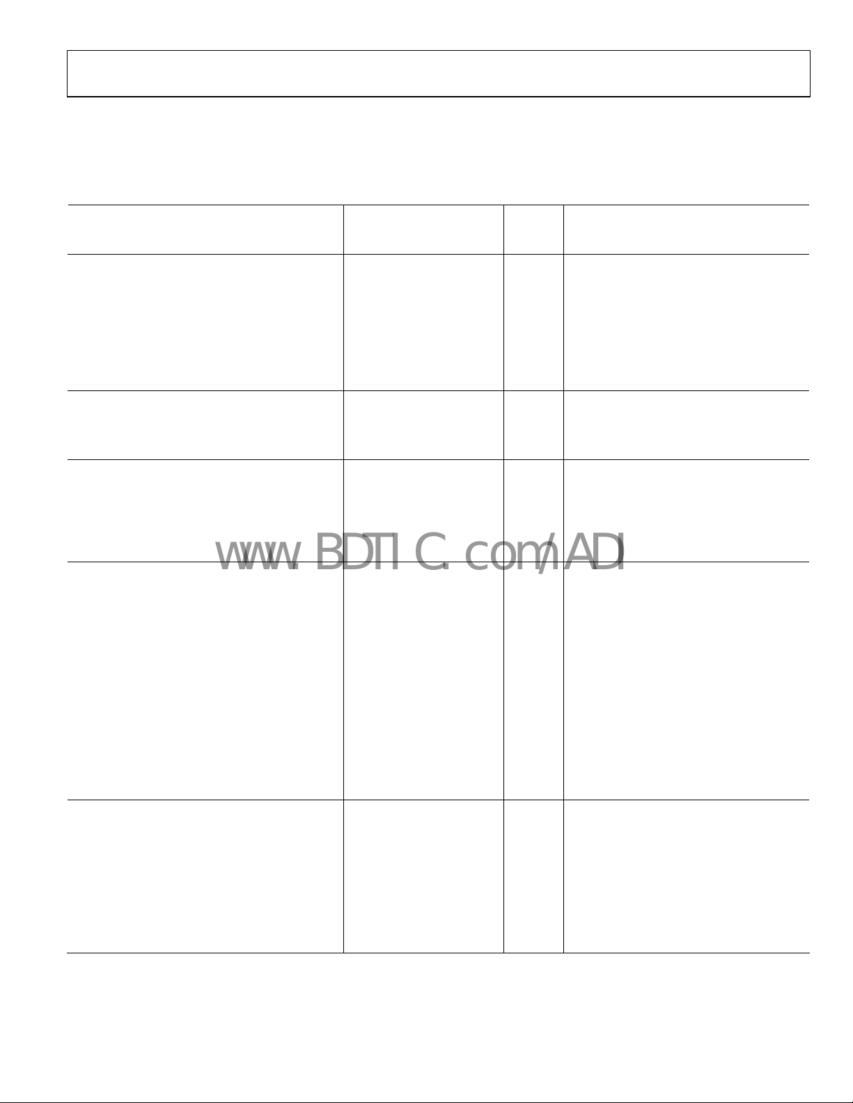
Table 1.
B Version
Parameter
+25°C
ANALOG SWITCH
Analog Signal Range VSS to V
On Resistance (RON) 130 230 Ω typ VS = ±10 V, IS = −10 mA; see Figure 11
200 Ω max VDD = +13.5 V, VSS = −13.5 V
On Resistance Match Between Channels (∆RON) 5 Ω typ VS = ±10 V, IS = −10 mA
10 Ω max
On Resistance Flatness (R
) 25 Ω typ VS = −5 V, 0 V, +5 V; IS = −10 mA
FLAT (ON)
65 Ω max
LEAKAGE CURRENTS VDD = +16.5 V, VSS = −16.5 V
Source Off Leakage IS (Off) ±10 nA typ VD = ±10 V; VS = ±10 V; see Figure 12
Drain Off Leakage ID (Off) ±10 nA typ VD = ±10 V; VS = ±10 V; see Figure 12
Channel On Leakage ID, IS (On) ±10 nA typ VS = VD = ±10 V; see Figure 13
DIGITAL INPUTS
Input High Voltage, V
Input Low Voltage, V
Input Current, I
INL
2.0 V min
INH
0.8 V max
INL
or I
±0.005 μA typ VIN = V
INH
±0.1 μA max
Digital Input Capacitance, C
IN
5 pF typ
DYNAMIC CHARACTERISTICS2
T
ON
110 ns typ RL = 300 Ω, CL = 35 pF
130 150 ns max VS = 10 V; see Figure 14
T
65 ns typ RL = 300 Ω, CL = 35 pF
OFF
85 95 ns max VS = 10 V; see Figure 14
T
25 ns typ RL = 300 Ω, CL = 35 pF
BBM
10 ns min VS1 = VS2 = +10 V; see Figure 15
Charge Injection 2 pC typ VS = 0 V, RS = 0 Ω, CL = 1 nF; see Figure 16
Off Isolation 80 dB typ RL = 50 Ω, CL = 5 pF, f = 1 MHz; see Figure 17
Channel-to-Channel Crosstalk 85 dB typ RL = 50 Ω, CL = 5 pF, f = 1 MHz; see Figure 19
−3 dB Bandwidth 700 MHz typ RL = 50 Ω, CL = 5 pF; see Figure 18
CS (Off) 5 pF typ f = 1 MHz; VS = 0 V
CD (Off) 5 pF typ f = 1 MHz; VS = 0 V
CD, CS (On) 10 pF typ f = 1 MHz; VS = 0 V
POWER REQUIREMENTS VDD = +16.5 V, VSS = −16.5 V
IDD 0.002 μA typ Digital inputs = 0 V or V
1 μA max
IDD 260 μA typ Digital inputs = 5 V
400 μA max
I
SS
0.002 μA typ Digital inputs = 0 V or V
1 μA max
ISS 0.002 μA typ Digital inputs = 5 V
1 μA max
1
Temperature range is B Version: −40°C to +105°C.
2
Guaranteed by design, not subject to production test.
−40°C to
+105
°C
DD
Unit Test Conditions/Comments
V
or V
INL
INH
DD
DD
Rev. 0 | Page 3 of 12

ADG1334
www.BDTIC.com/ADI
SINGLE SUPPLY1
VDD = 12 V ± 10%, VSS = 0 V, GND = 0 V, unless otherwise noted.
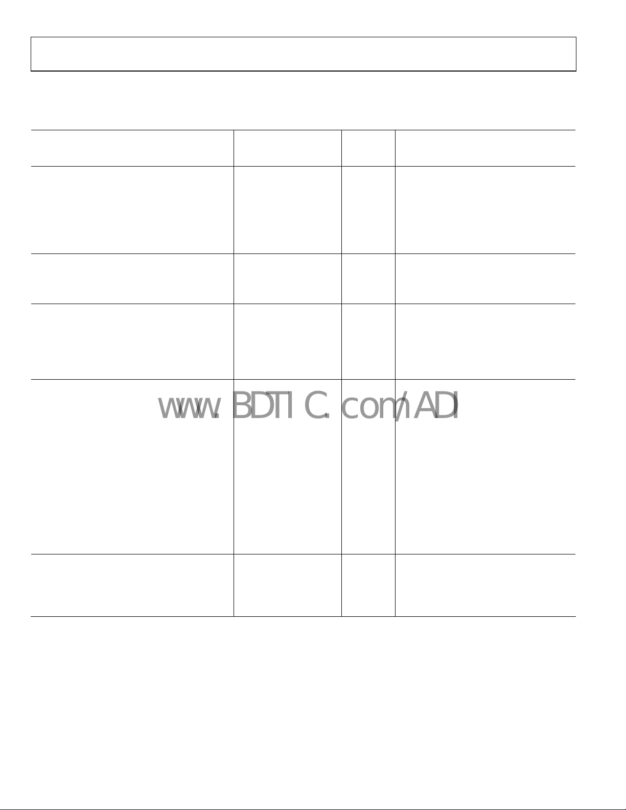
Table 2.
B Version
−40°C to
+105
Parameter +25°C
ANALOG SWITCH
Analog Signal Range 0 to V
On Resistance (RON) 325 520 Ω typ VS = 0 V to10 V, IS = −10 mA; see Figure 11
500 Ω max VDD = 10.8 V, VSS = 0 V
On Resistance Match Between Channels (∆RON) 10 Ω typ VS = 0 V to10 V, IS = −10 mA
20 Ω max
On Resistance Flatness (R
) 65 Ω typ VS = 3 V, 6 V, 9 V, IS = −10 mA
FLAT(ON)
LEAKAGE CURRENTS VDD = 13.2 V
Source Off Leakage IS (Off) ±10 nA typ VS = 1 V/10 V, VD = 10 V/1 V; see Figure 12
Drain Off Leakage ID (Off) ±10 nA typ VS = 1 V/10 V, VD = 10 V/1 V; see Figure 12
Channel On Leakage ID, IS (On) ±10 nA typ VS = VD = 1 V or 10 V, see Figure 13
DIGITAL INPUTS
Input High Voltage, V
Input Low Voltage, V
Input Current, I
or I
INL
INH
INL
INH
2.0 V min
0.8 V max
±0.005 μA typ VIN = V
±0.1 μA max
Digital Input Capacitance, C
DYNAMIC CHARACTERISTICS
T
ON
IN
2
3 pF typ f = 1 MHz
135 ns typ RL = 300 Ω, CL = 35 pF
170 200 ns max VS = 8 V; see Figure 14
T
OFF
95 ns typ RL = 300 Ω, CL = 35 pF
115 140 ns max VS = 8 V; see Figure 14
T
BBM
50 ns typ RL = 300 Ω, CL = 35 pF
10 ns min VS1 = VS2 = 8 V; see Figure 15
Charge Injection 2 pC typ VS = 6 V, RS = 0 Ω, CL = 1 nF; see Figure 16
Off Isolation 80 dB typ RL = 50 Ω, CL = 5 pF, f = 1 MHz; see Figure 17
Channel-to-Channel Crosstalk 85 dB typ RL = 50 Ω, CL = 5 pF, f = 1 MHz; see Figure 19
−3 dB Bandwidth 500 MHz typ RL = 50 Ω, CL = 5 pF; see Figure 18
CS (Off) 5 pF typ f = 1 MHz; VS = 6 V
CD (Off) 5 pF typ f = 1 MHz; VS = 6 V
CD, CS (On) 10 pF typ f = 1 MHz; VS = 6 V
POWER REQUIREMENTS VDD = 13.2 V
I
DD
0.002 μA typ Digital inputs = 0 V or V
1 μA max
I
DD
260 μA typ Digital inputs = 5 V
420 μA max
1
Temperature range is B Version: −40°C to +105°C.
2
Guaranteed by design, not subject to production test.
°C
DD
Unit Test Conditions/Comments
V
or V
INL
INH
DD
Rev. 0 | Page 4 of 12
 Loading...