

www.BDTIC.com/ADI
±15 V/12 V Quad SPST Switches
ADG1311/ADG1312/ADG1313
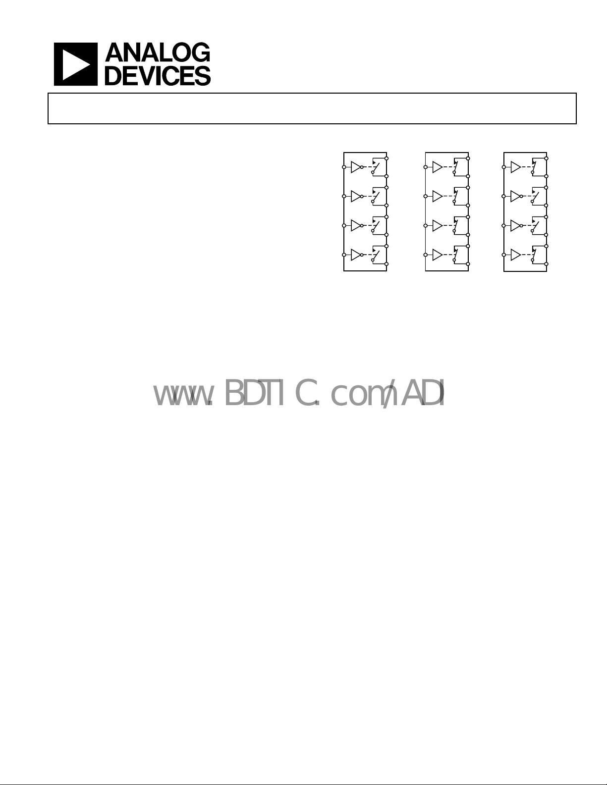
FEATURES FUNCTIONAL BLOCK DIAGRAM
33 V supply range
Fully specified at +12 V, ±15 V
130 Ω on resistance
supply required
No V
L
3 V logic-compatible inputs
Rail-to-rail operation
16-lead TSSOP and 16-lead SOIC
Typical power consumption: <0.03 μW
APPLICATIONS
Signal switching
Battery-powered systems
Communication systems
Audio/video signal routing
IN1
IN2
ADG1311
IN3
IN4
S1
IN1
D1
S2
IN2
D2
S3
D3
S4
D4
SWITCHES SHOWN FOR A LOGIC 1 INPUT
ADG1312
IN3
IN4
Figure 1.
S1
IN1
D1
S2
IN2
D2
S3
IN3
D3
S4
IN4
D4
ADG1313
GENERAL DESCRIPTION PRODUCT HIGHLIGHTS
The ADG1311/ADG1312/ADG1313 are monolithic CMOS
vices containing four independently selectable switches
de
designed on a CMOS process.
1. 3 V logic-compatible digital inputs: V
logic power supply required.
V
2. No
3. 16-lead TSSO
L
P and SOIC packages.
= 2.0 V, VIL = 0.8 V.
IH
S1
D1
S2
D2
S3
D3
S4
D4
05676-001
The ADG1311/ADG1312/ADG1313 contain four independent
s
ingle-pole/single-throw (SPST) switches. The ADG1311 and
ADG1312 differ only in that the digital control logic is inverted.
The ADG1311 switches are turned on with Logic 0 on the appropriate control input, while Logic 1 is required for the ADG1312.
The ADG1313 has two switches with digital control logic similar
to the ADG1311; the logic is inverted on the other two switches.
The ADG1313 exhibits break-before-make switching action for
use in multiplexer applications.
Each switch conducts equally well in both
directions when on
and has an input signal range that extends to the supplies. In the
off condition, signal levels up to the supplies are blocked.
Rev. 0
Information furnished by Analog Devices is believed to be accurate and reliable. However, no
responsibility is assumed by Anal og Devices for its use, nor for any infringements of patents or ot her
rights of third parties that may result from its use. Specifications subject to change without notice. No
license is granted by implication or otherwise under any patent or patent rights of Analog Devices.
Trademarks and registered trademarks are the property of their respective owners.
One Technology Way, P.O. Box 9106, Norwood, MA 02062-9106, U.S.A.
Tel: 781.329.4700 www.analog.com
Fax: 781.461.3113 © 2005 Analog Devices, Inc. All rights reserved.

ADG1311/ADG1312/ADG1313
www.BDTIC.com/ADI
TABLE OF CONTENTS
Features.............................................................................................. 1
Absolute Maximum Ratings ............................................................5
Applications....................................................................................... 1
Functional Block Diagram .............................................................. 1
General Description ......................................................................... 1
Product Highlights ........................................................................... 1
Specifications..................................................................................... 3
Dual Supply................................................................................... 3
Single Supply................................................................................. 4
REVISION HISTORY
10/05—Revision 0: Initial Version
ESD Caution...................................................................................5
Pin Configuration and Function Descriptions..............................6
Terminology.......................................................................................7
Typical Performance Characteristics..............................................8
Test Circuits..................................................................................... 10
Outline Dimensions....................................................................... 12
Ordering Guide .......................................................................... 12
Rev. 0 | Page 2 of 12
ADG1311/ADG1312/ADG1313
www.BDTIC.com/ADI
SPECIFICATIONS
DUAL SUPPLY
VDD = 15 V ± 10%, VSS = −15 V± 10%, GND = 0 V, unless otherwise noted.
Table 1.
Y Version
Parameter 25°C −40°C to +105°C Unit Test Conditions/Comments
ANALOG SWITCH
Analog Signal Range VDD to VSS V
On Resistance (RON) 130 230 Ω typ VS = ±10 V, IS = −1 mA; Figure 10
200 Ω max VDD = +13.5 V, VSS = −13.5 V
On Resistance Match Between
Channels (∆R
)
ON
5 Ω typ V
10 Ω max
On Resistance Flatness (R
) 25 Ω typ VS = −5 V/0 V/+5 V; IS = −1 mA
FLAT(ON)
65 Ω max
LEAKAGE CURRENTS VDD = +16.5 V, VSS = −16.5 V
Source Off Leakage, IS (Off) ±10 nA typ
Drain Off Leakage, ID (Off) ±10 nA typ
Channel On Leakage, ID, IS (On) ±10 nA typ VS = VD = ±10 V; Figure 12
DIGITAL INPUTS
Input High Voltage, V
Input Low Voltage, V
Input Current, I
INL
2.0 V min
INH
0.8 V max
INL
or I
0.005 μA typ VIN = V
INH
±0.1 μA max
Digital Input Capacitance, CIN 2.5 pF typ
DYNAMIC CHARACTERISTICS2
tON 105 ns typ RL = 300 Ω, CL = 35 pF
125 180 ns max VS = +10 V; Figure 13
t
40 ns typ RL = 300 Ω, CL = 35 pF
OFF
50 60 ns max VS = +10 V; Figure 13
Break-Before-Make Time Delay, tD 25 ns typ RL = 300 Ω, CL = 35 pF
(ADG1313 Only) 10 ns min VS1 = VS2 = 10 V; Figure 14
Charge Injection 2 pC typ VS = 0 V, RS = 0 Ω, CL = 1 nF; Figure 15
Off Isolation 80 dB typ RL = 50 Ω, CL = 5 pF, f = 1 MHz; Figure 16
Channel-to-Channel Crosstalk 90 dB typ RL = 50 Ω, CL = 5 pF, f = 1 MHz; Figure 17
−3 dB Bandwidth 600 MHz typ RL = 50 Ω, CL = 5 pF; Figure 18
CS (Off) 5 pF typ
CD (Off) 5 pF typ
CD, CS (On) 10 pF typ
POWER REQUIREMENTS VDD = +16.5 V, VSS = −16.5 V
IDD 0.001 μA typ Digital inputs = 0 V or VDD
1.0 μA max
IDD 220 μA typ Digital inputs = 5 V
320 μA max
ISS 0.001 μA typ Digital inputs = 0 V or VDD
1.0 μA max
ISS 0.001 μA typ Digital inputs = 5 V
1.0 μA max
1
Temperature range for Y Version is −40°C to +105°C.
2
Guaranteed by design, not subject to production test.
1
= ±10 V, IS = −1 mA
S
VS = ±10 V, VD = ∓10 V; Figure 11
V
= ±10V, VD = ∓10 V; Figure 11
S
or V
INH
INL
Rev. 0 | Page 3 of 12
ADG1311/ADG1312/ADG1313
www.BDTIC.com/ADI
SINGLE SUPPLY
VDD = 12 V ± 10%, VSS = 0 V, GND = 0 V, unless otherwise noted.
Table 2.
Y Version
Parameter 25°C −40°C to +105°C Unit Test Conditions/Comments
ANALOG SWITCH
Analog Signal Range 0 V to VDD V
On Resistance (RON) 325 520 Ω typ VS = 0 V − 10 V, IS = −1 mA; Figure 10
500 Ω max VDD = 10.8 V, VSS = 0 V
On Resistance Match Between
Channels (∆R
)
ON
10 Ω typ V
15 Ω max
On Resistance Flatness (R
) 65 Ω typ VS = +3 V/+6 V/+9 V, IS = −1 mA
FLAT(ON)
LEAKAGE CURRENTS VDD = 13.2 V, VSS = 0 V
Source Off Leakage, IS (Off) ±10 nA typ VS = +1 V/+10 V, VD = +10 V/+1 V; Figure 11
Drain Off Leakage, ID (Off) ±10 nA typ VS = +1 V/+10 V, VD = +10 V/+1 V Figure 11
Channel On Leakage, ID, IS (On) ±10 nA typ VS = VD = +1 V or +10 V; Figure 12
DIGITAL INPUTS
Input High Voltage, V
Input Low Voltage, V
Input Current, I
INL
2.0 V min
INH
0.8 V max
INL
or I
0.001 μA typ VIN = V
INH
±0.1 μA max
Digital Input Capacitance, CIN 3 pF typ
DYNAMIC CHARACTERISTICS2
tON 120 ns typ RL = 300 Ω, CL = 35 pF
155 210 ns max VS = 8 V; Figure 13
t
45 ns typ RL = 300 Ω, CL = 35 pF
OFF
65 80 ns max VS = 8 V; Figure 13
Break-Before-Make Time Delay, tD 50 ns typ RL = 300 Ω, CL = 35 pF
(ADG1313 Only) 10 ns min VS1 = VS2 = 8 V; Figure 14
Charge Injection 2 pC typ VS = 6 V, RS = 0 Ω, CL = 1 nF; Figure 15
Off Isolation 80 dB typ RL = 50 Ω, CL = 5 pF, f = 1 MHz; Figure 16
Channel-to-Channel Crosstalk 90 dB typ RL = 50 Ω, CL = 5 pF, f = 1 MHz; Figure 17
−3 dB Bandwidth 500 MHz typ RL = 50 Ω, CL = 5 pF; Figure 18
CS (Off) 5 pF typ
CD (Off) 5 pF typ
CD, CS (On) 10 pF typ
POWER REQUIREMENTS VDD = 13.2 V
IDD 0.001 μA typ Digital inputs = 0 V or VDD
1.0 μA max
IDD 220 μA typ Digital inputs = 5 V
320 μA max
1
Temperature range for Y Version is −40°C to +105°C.
2
Guaranteed by design, not subject to production test.
1
= 0 V − 10 V, IS = −1 mA
S
or V
INL
INH
Rev. 0 | Page 4 of 12
ADG1311/ADG1312/ADG1313
www.BDTIC.com/ADI
ABSOLUTE MAXIMUM RATINGS
TA = 25°C, unless otherwise noted.
Table 3.
Parameter Rating
VDD to VSS 35 V
VDD to GND −0.3 V to +25 V
VSS to GND +0.3 V to −25 V
Analog Inputs
Digital Inputs
Peak Current, S or D
Continuous Current per
Channe
Operating Temperature Range
Automotive −40°C to +105°C
Storage Temperature Range −65°C to +150°C
Junction Temperature 150°C
16-Lead TSSOP, θ
Impedance (4-layer board)
16-Lead SOIC, θ
Impedance
Reflow Soldering Peak
Temperature, Pb free
1
Overvoltages at IN, S, or D are clamped by internal diodes. Current should be
limited to the maximum ratings given.
1
1
l, S or D
JA
Thermal
JA
Thermal
− 0.3 V to VDD + 0.3 V or
V
SS
30 mA, whichever occurs first
GND − 0.3 V to V
30 mA, whichever occurs first
100 mA (pulsed at 1 ms,
10% duty c
25 mA
112°C/W
77°C/W
260°C
+ 0.3 V or
DD
ycle max)
Stresses above those listed under Absolute Maximum Ratings
ma
y cause permanent damage to the device. This is a stress
rating only; functional operation of the device at these or any
other conditions above those indicated in the operational
section of this specification is not implied. Exposure to absolute
maximum rating conditions for extended periods may affect
device reliability.
Table 4. ADG1311/ADG1312 Truth Table
ADG1311 INx ADG1312 INx Switch Condition
0 1 On
1 0 Off
Table 5. ADG1313 Truth Table
ADG1313 INx Switch 1, 4 Switch 2, 3
0 Off On
1 On Off
ESD CAUTION
ESD (electrostatic discharge) sensitive device. Electrostatic charges as high as 4000 V readily accumulate on
the human body and test equipment and can discharge without detection. Although this product features
proprietary ESD protection circuitry, permanent damage may occur on devices subjected to high energy
electrostatic discharges. Therefore, proper ESD precautions are recommended to avoid performance
degradation or loss of functionality.
Rev. 0 | Page 5 of 12

ADG1311/ADG1312/ADG1313
www.BDTIC.com/ADI
PIN CONFIGURATION AND FUNCTION DESCRIPTIONS
1
IN1
2
D1
3
S1
ADG1311/
4
V
GND
IN4 IN3
ADG1312/
SS
ADG1313
5
TOP VIEW
6
S4
7
D4
8
NC = NO CONNECT
16
IN2
15
D2
14
S2
13
V
DD
12
NC
11
S3
10
D3
9
05676-002
Figure 2. SOIC/TSSOP Pin Configuration
Table 6. Pin Function Descriptions
Pin No. Mnemonic Description
1 IN1 Logic Control Input.
2 D1 Drain Terminal. Can be an input or output.
3 S1
4 V
Most Negative Power Supply Potential.
SS
5 GND
6 S4
7 D4
8 IN4
9 IN3
10 D3
11 S3
12 NC
13 V
Most Positive Power Supply Potential.
DD
14 S2
15 D2
Source Terminal. Can be an input or output.
Ground (0 V) Reference.
Source Terminal. Can be an input or output.
Drain Terminal. Can be an input or output.
Logic Control Input.
Logic Control Input.
Drain Terminal. Can be an input or output.
Source Terminal. Can be an input or output.
No Connection.
Source Terminal. Can be an input or output.
Drain Terminal. Can be an input or output.
16 IN2 Logic Control Input.
Rev. 0 | Page 6 of 12

ADG1311/ADG1312/ADG1313
www.BDTIC.com/ADI
TERMINOLOGY
IDD
The positive supply current.
, CS (On)
C
D
The on switch capacitance, measured with reference to ground.
I
SS
The negative supply current.
(VS)
V
D
The analog voltage on Terminal D and Terminal S.
R
ON
The ohmic resistance between D and S.
R
FLAT(ON)
Flatness is defined as the difference between the maximum and
inimum value of on resistance, as measured over the specified
m
analog signal range.
I
(Off)
S
The source leakage current with the switch off.
I
(Off)
D
The drain leakage current with the switch off.
I
, IS (On)
D
The channel leakage current with the switch on.
V
INL
The maximum input voltage for Logic 0.
V
INH
The minimum input voltage for Logic 1.
(I
INL
INH
)
I
The input current of the digital input.
C
(Off)
S
The off switch source capacitance, measured with reference to
round.
g
C
IN
The digital input capacitance.
t
ON
The delay between applying the digital control input and the
switching on. See Figure 13.
output
t
OFF
The delay between applying the digital control input and the
switching off. See Figure 13.
output
Charge Injection
A measure of the glitch impulse transferred from the digital
put to the analog output during switching.
in
Off Isolation
A measure of unwanted signal coupling through an off switch.
Crosstalk
A measure of unwanted signal that is coupled through from one
cha
nnel to another as a result of parasitic capacitance.
Bandwidth
The frequency at which the output is attenuated by 3 dB.
On Response
The frequency response of the on switch.
Insertion Loss
The loss due to the on resistance of the switch.
(Off)
C
D
The off switch drain capacitance, measured with reference to
round.
g
Rev. 0 | Page 7 of 12

ADG1311/ADG1312/ADG1313
www.BDTIC.com/ADI
TYPICAL PERFORMANCE CHARACTERISTICS
200
TA = 25°C
180
160
140
120
100
80
ON RESISTANCE (Ω)
60
40
20
0
–15 –12 –9 –6 –3 3 90 6 12 15
Figure 3. On Resistance as a Function of V
VDD = +15V
= –15V
V
SS
SOURCE OR DRAIN VOLTAGE (V)
(VS) for Dual Supply Figure 6. On Resistance as a Function of VD (VS) for Different
D
05676-008
600
VDD = 12V
V
= 0V
SS
500
TA = +85°C
400
300
200
ON RESISTANCE (Ω)
100
0
02468101
TA = –40°C
SOURCE OR DRAIN VOLTAGE (V)
TA = +25°C
Temperatures, Single Supply
05676-007
2
450
TA = 25°C
400
350
300
250
200
150
ON RESISTANCE (Ω)
100
50
0
02468101
SOURCE OR DRAIN VOLTAGE (V)
Figure 4. On Resistance as a Function of V
250
VDD = +15V
= –15V
V
SS
200
150
100
ON RESISTANCE (Ω)
50
0
–15 –10 –5 0 5 10 15
TA = –40°C
SOURCE OR DRAIN VOLTAGE (V)
Figure 5. On Resistance as a Function of V
VDD = 12V
= 0V
V
SS
TA = +85°C
(VS) for Single Supply Figure 7. TON/T
D
TA = +25°C
(VS) for Different
D
Temperatures, Dual Supply
200
180
12V SS T
OFF
ON
15V DS T
15V DS T
ON
OFF
160
140
120
100
TIME (ns)
80
60
40
20
05676-005
2
0
–40 –20 40200 60 80 100 120
0
VDD = +15V
05676-006
–10
–20
–30
–40
–50
–60
–70
OFF ISOLATION (dB)
–80
–90
–100
–110
= –15V
V
SS
= 25°C
T
A
10k 100k 1M 10M 100M 1G
12V SS T
TEMPERATURE (°C)
Times vs. Temperature
OFF
FREQUENCY (Hz)
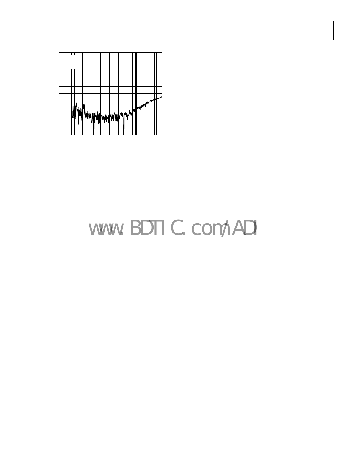
Figure 8. Off Is olation v s. Frequency
05676-016
05676-017
Rev. 0 | Page 8 of 12
ADG1311/ADG1312/ADG1313
www.BDTIC.com/ADI
0
VDD = +15V
–10
= –15V
V
SS
= 25°C
–20
T
A
–30
–40
–50
–60
–70
CROSSTALK (dB)
–80
–90
–100
–110
–120
10k 100k 1M 10M 100M
FREQUENCY (Hz)
05676-018
Figure 9. Crosstalk v s. Frequency
Rev. 0 | Page 9 of 12

ADG1311/ADG1312/ADG1313
V
V
V
www.BDTIC.com/ADI
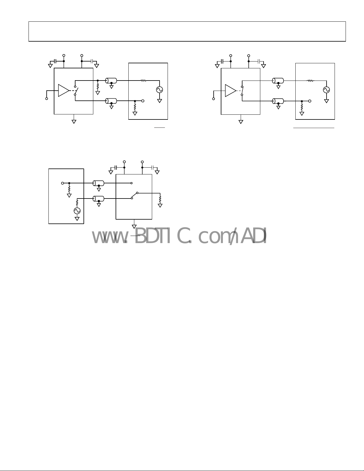
TEST CIRCUITS
I
DS
V1
SD
IS (OFF) ID (OFF)
SD
A A
SD
NC
ID (ON)
A
V
S
RON = V1/I
DS
05676-020
S
V
D
05676-021
NC = NO CONNECT
Figure 10. Test Circuit 1—On Resistance Figure 11. Test Circuit 2—Off Leakage Figure 12. Test Circuit 3 —On Leakage
V
V
DD
SS
0.1μF
V
DD
SD
V
S
IN
GND
0.1μF
ADG1312
V
V
SS
V
OUT
R
300Ω
C
L
L
35pF
IN
V
IN
V
OUT
ADG1311
50% 50%
50% 50%
90% 90%
t
ON
t
OFF
05676-023
Figure 13. Test Circuit 4—Switching Times
V
V
DD
SS
0.1μF
V
DD
IN1,
IN2
S1 D1
S2 D2
ADG1313
GND
S1
S2
0.1μF
V
SS
V
OUT1
C
R
L
300Ω
C
L
35pF
V
OUT2
R
300Ω
L
L
35pF
Figure 14. Test Circuit 5—Break-Before-Make Time Delay
V
V
V
OUT1
OUT2
IN
0V
0V
0V
50% 50%
90%
90%
t
D
t
90%
90%
D
V
D
05676-024
05676-022
V
V
DD
SS
V
V
DD
SS
C
1nF
V
OUT
L
R
S
V
S
SD
IN
GND
Figure 15. Test Circuit 6—Charge Injection
Rev. 0 | Page 10 of 12
V
IN
V
IN
V
OUT
ADG1312
ADG1311
Q
INJ
ON
= CL×ΔV
OUT
OFF
ΔV
OUT
05676-025
ADG1311/ADG1312/ADG1313
www.BDTIC.com/ADI
V
0.1μF
V
DD
SS
0.1μF
0.1μF
V
V
DD
SS
0.1μF
V
IN
V
IN
V
DD
S
GND
SS
50Ω
D
OFF ISOLATION = 20 log
Figure 16. Test Circuit 7—Off Isolation Figure 18. Test Circuit 9—Bandwidth
V
DD
0.1μF
NETWORK
ANALYZER
V
OUT
R
L
50Ω
V
S
CHANNEL-TO-CHANNEL CROSSTALK = 20 log
V
DD
S1
S2
GND
V
Figure 17. Test Circuit 8—Channel-to-Channel Crosstalk
NETWORK
ANALYZER
50Ω
R
L
50Ω
V
SS
V
SS
OUT
V
S
V
OUT
D2
V
S
0.1μF
V
IN
V
IN
V
OUT
V
05676-026
S
V
DD
SS
S
D
GND
INSERTION LOSS = 20 log
NETWORK
ANALYZER
50Ω
R
L
50Ω
WITH SWITCH
V
OUT
V
WITHOUT SWITCH
OUT
V
S
V
OUT
05676-028
R
50Ω
05676-027
Rev. 0 | Page 11 of 12
ADG1311/ADG1312/ADG1313
www.BDTIC.com/ADI
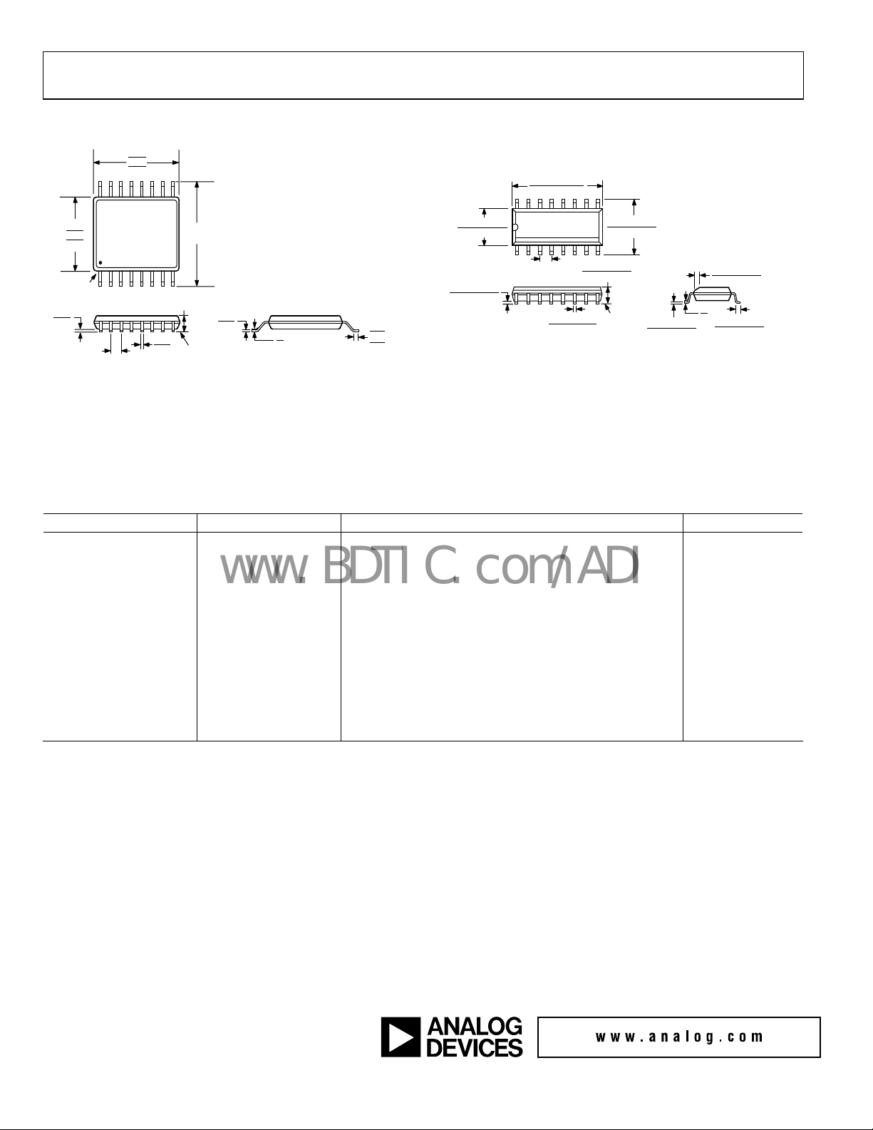
OUTLINE DIMENSIONS
5.10
5.00
4.90
16
4.50
4.40
4.30
PIN 1
0.15
0.05
0.65
BSC
COPLANARITY
COMPLIANT TO JEDEC STANDARDS MO-153-AB
Figure 19. 16-Lead Thin Shrink S
9
6.40
BSC
81
1.20
0.10
0.30
0.19
MAX
SEATING
PLANE
0.20
0.09
mall Outline Package [TSSOP]
(RU-16)
Dimensions shown in millimeters
8°
0°
0.75
0.60
0.45
10.00 (0.3937)
9.80 (0.3858)
4.00 (0.1575)
3.80 (0.1496)
0.25 (0.0098)
0.10 (0.0039)
COPLANARITY
CONTROLLING DIMENSIONS ARE IN MILLIMETERS; INCH DIMENSIONS
(IN PARENTHESES) ARE ROUNDED-OFF MILLIMETER EQUIVALENTS FOR
REFERENCE ONLY AND ARE NOT APPROPRIATE FOR USE IN DESIGN
16
1
1.27 (0.0500)
BSC
0.51 (0.0201)
0.10
0.31 (0.0122)
COMPLIANT TO JEDEC STANDARDS MS-012-AC
9
6.20 (0.2441)
5.80 (0.2283)
8
1.75 (0.0689)
1.35 (0.0531)
SEATING
PLANE
0.25 (0.0098)
0.17 (0.0067)
0.50 (0.0197)
0.25 (0.0098)
8°
0°
1.27 (0.0500)
0.40 (0.0157)
× 45°
Figure 20. 16-Lead Standard Small Outline Package [SOIC_N]
row Body
Nar
(R-16)
Dimensions shown in millimeters and (inches)
ORDERING GUIDE
Model Temperature Range Package Description Package Option
ADG1311YRUZ −40°C to +105°C 16-Lead Thin Shrink Small Outline Package [TSSOP] RU-16
ADG1311YRUZ-REEL7 −40°C to +105°C 16-Lead Thin Shrink Small Outline Package [TSSOP] RU-16
ADG1311YRZ −40°C to +105°C 16-Lead Narrow Body Small Outline Package [SOIC_N] R-16
ADG1311YRZ-REEL7 −40°C to +105°C 16-Lead Narrow Body Small Outline Package [SOIC_N] R-16
ADG1312YRUZ −40°C to +105°C 16-Lead Thin Shrink Small Outline Package [TSSOP] RU-16
ADG1312YRUZ-REEL7 −40°C to +105°C 16-Lead Thin Shrink Small Outline Package [TSSOP] RU-16
ADG1312YRZ1 −40°C to +105°C 16-Lead Narrow Body Small Outline Package [SOIC_N] R-16
ADG1312YRZ-REEL7 −40°C to +105°C 16-Lead Narrow Body Small Outline Package [SOIC_N]
ADG1313YRUZ −40°C to +105°C 16-Lead Thin Shrink Small Outline Package [TSSOP] RU-16
ADG1313YRUZ-REEL7 −40°C to +105°C 16-Lead Thin Shrink Small Outline Package [TSSOP] RU-16
ADG1313YRZ1 −40°C to +105°C 16-Lead Narrow Body Small Outline Package [SOIC_N] R-16
ADG1313YRZ-REEL7 −40°C to +105°C 16-Lead Narrow Body Small Outline Package [SOIC_N] R-16
1
Z = Pb-free part.
1
1
1
1
1
1
1
1
1
1
R-16
© 2005 Analog Devices, Inc. All rights reserved. Trademarks and
registered trademarks are the property of their respective owners.
D05676-0-10/05(0)
Rev. 0 | Page 12 of 12
 Loading...