

Low Capacitance, Low Charge Injection,
FEATURES
<0.5 pC charge injection over full signal range
Off capacitance: 2 pF
Off leakage: 20 pA
Supply range: 33 V
On resistance: 120 Ω
Fully specified at ±15 V, +12 V
No V
supply required
L
3 V logic-compatible inputs
Rail-to-rail operation
10-lead MSOP package
APPLICATIONS
Automatic test equipment
Data acquisition systems
Battery-powered systems
Sample-and-hold systems
Audio signal routing
Video signal routing
Communication systems
±15 V/+12 V iCMOS
ADG1221/ADG1222/ADG1223
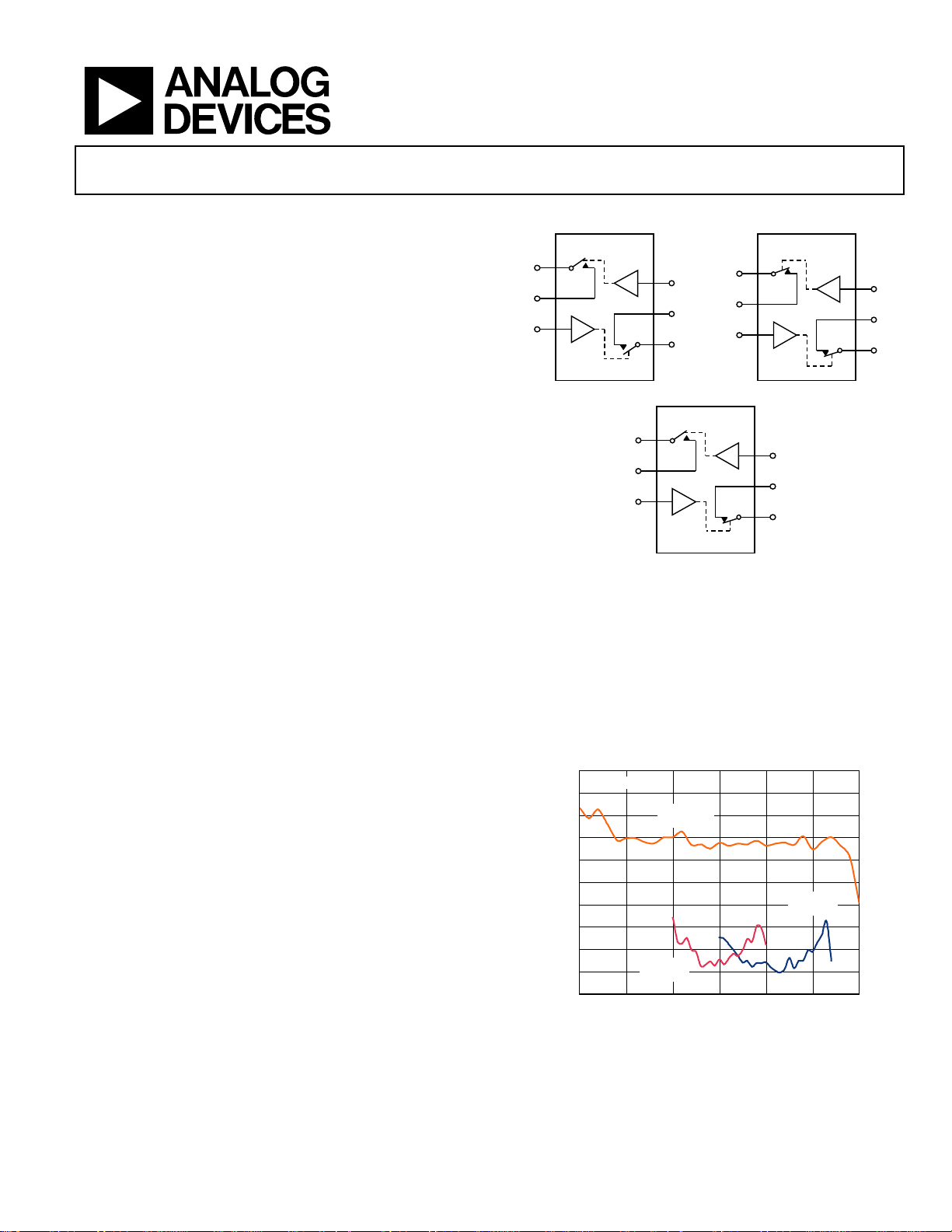
FUNCTIONAL BLOCK DIAGRAM
ADG1221
S1
D1
IN2
®
Dual SPST Switches
ADG1222
S1
IN1
D1
D2
IN2
S2
ADG1223
S1
D1
IN2
SWITCHES SHOW N FOR A LOGIC 0 INPUT
Figure 1.
IN1
D2
S2
IN1
D2
S2
06574-001
GENERAL DESCRIPTION
The ADG1221/ADG1222/ADG1223 are monolithic, complementary metal-oxide semiconductor (CMOS) devices containing
four independently selectable switches designed on an iCMOS
(industrial CMOS) process. iCMOS is a modular manufacturing
process combining high voltage CMOS and bipolar technologies.
It enables the development of a wide range of high performance
analog ICs, capable of 33 V operation, in a footprint that no
previous generation of high voltage parts has been able to achieve.
Unlike analog ICs using conventional CMOS processes, iCMOS
components can tolerate high supply voltages while providing
increased performance, dramatically lower power consumption,
and reduced package size.
The ultralow capacitance and exceptionally low charge injection
of these switches make them ideal solutions for data acquisition
and sample-and-hold applications, where low glitch and fast
settling are required.
charge injection over the full signal range of the device.
The ADG1221/ADG1222/ADG1223 contain two independent
single-pole/single-throw (SPST) switches. The ADG1221 and
ADG1222 differ only in that the digital control logic is inverted.
The ADG1221 switches are turned on with Logic 1 on the appropriate control input, and Logic 0 is required for the
Figure 2 shows that there is minimum
ADG1222. The ADG1223 has one switch with digital control
logic similar to that of the ADG1221; the logic is inverted on
the other switch. The ADG1223 exhibits break-before-make
switching action for use in multiplexer applications. Each
switch conducts equally well in both directions when on and
has an input signal range that extends to the supplies. In the off
condition, signal levels up to the supplies are blocked.
0.5
TA = 25ºC
0.4
0.3
0.2
0.1
0
–0.1
–0.2
CHARGE INJECTI ON (pC)
–0.3
–0.4
–0.5
–15 15
Figure 2. Charge Injection vs. Input Voltage
VDD = +15V
= –15V
V
SS
VDD = 12V
V
SS
VDD = +5V
= –5V
V
SS
–10 –5 0 5 10
INPUT VOLTAGE (V)
= 0V
06574-041
Rev. 0
Information furnished by Analog Devices is believed to be accurate and reliable. However, no
responsibility is assumed by Anal og Devices for its use, nor for any infringements of patents or ot her
rights of third parties that may result from its use. Specifications subject to change without notice. No
license is granted by implication or otherwise under any patent or patent rights of Analog Devices.
Trademarks and registered trademarks are the property of their respective owners.
One Technology Way, P.O. Box 9106, Norwood, MA 02062-9106, U.S.A.
Tel: 781.329.4700 www.analog.com
Fax: 781.461.3113 ©2007 Analog Devices, Inc. All rights reserved.

ADG1221/ADG1222/ADG1223
TABLE OF CONTENTS
Features.............................................................................................. 1
Applications....................................................................................... 1
Functional Block Diagram .............................................................. 1
General Description ......................................................................... 1
Revision History ............................................................................... 2
Specifications..................................................................................... 3
Dual Supply................................................................................... 3
Single Supply................................................................................. 4
Absolute Maximum Ratings............................................................ 6
Thermal Resistance ...................................................................... 6
ESD Caution.................................................................................. 6
REVISION HISTORY
2/07—Rev. 0: Initial Version
Pin Configuration and Function Descriptions..............................7
Terminology.......................................................................................8
Typical Performance Characteristics..............................................9
Test Circuits..................................................................................... 13
Outline Dimensions....................................................................... 15
Ordering Guide......................................................................... 15
Rev. 0 | Page 2 of 16

ADG1221/ADG1222/ADG1223
SPECIFICATIONS
DUAL SUPPLY
VDD = 15 V ± 10%, VSS = –15 V ± 10%, GND = 0 V, unless otherwise noted.
Table 1.
Temperature
Parameter 25°C –40°C to +85°C –40°C to +125°C Unit Test Conditions/Comments
ANALOG SWITCH
Analog Signal Range VDD to VSS V
On Resistance, RON
120 Ω typ
200 240 270 Ω max
On Resistance Match
Between Channels, ∆R
ON
V
2.5 Ω typ
6 10 12 Ω max
On Resistance Flatness, R
VS = –5 V/0 V/+5 V; IS = –1 mA
FLAT(ON)
20 Ω typ
64 76 83 Ω max
LEAKAGE CURRENTS VDD = +16.5 V, VSS = –16.5 V
Source Off Leakage, IS (Off) VS = ±10 V, VD = ±10 V (see Figure 24)
±0.002 nA typ
±0.1 ±0.6 ±1 nA max
Drain Off Leakage, ID (Off) VS = ±10 V, VD = ±10 V (see Figure 24)
±0.002 nA typ
±0.1 ±0.6 ±1 nA max
Channel On Leakage, ID, IS (On) VS = VD = ±10 V (see Figure 25)
±0.01 nA typ
±0.2 ±0.6 ±1 nA max
DIGITAL INPUTS
Input High Voltage, V
Input Low Voltage, V
Input Current, I
INL
2.0 V min
INH
0.8 V max
INL
or I
V
INH
0.005 μA typ
±0.1 μA max
Digital Input Capacitance, CIN 2.5 pF typ
DYNAMIC CHARACTERISTICS
1
tON
130 ns typ
170 210 240 ns max
t
OFF
85 ns typ
105 130 140 ns max
Break-Before-Make Time Delay
(ADG1223 Only), t
BBM
40 ns typ
10 ns min
Charge Injection, Q
0.1 pC typ VS = 0 V, RS = 0 Ω, CL = 1 nF (see Figure 28)
INJ
Off Isolation 75 dB typ
= +13.5 V, VSS = –13.5 V,
V
DD
V
= ±10 V, IS = –1 mA (see Figure 23)
S
= ±10 V, IS = –1 mA
S
= V
or V
IN
INL
= 300 Ω, CL = 35 pF, VS = 10 V
R
L
Figure 26)
(see
= 300 Ω, CL = 35 pF, VS = 10 V
R
L
Figure 26)
(see
= 300 Ω, CL = 35 pF, VS1 = VS2 = 10 V
R
L
(see
Figure 27)
= 50 Ω, CL = 1 pF, f = 1 MHz
R
L
Figure 29)
(see
INH
Rev. 0 | Page 3 of 16

ADG1221/ADG1222/ADG1223
Temperature
Parameter 25°C –40°C to +85°C –40°C to +125°C Unit Test Conditions/Comments
Channel-to-Channel
Crosstalk
Tot al H a r m onic
Distortion + Noise, THD + N
–3 dB Bandwidth 960 MHz typ RL = 50 Ω, CL = 1 pF (see Figure 31)
CS (Off) VS = 0 V, f = 1 MHz
1.7 pF typ
2.2 pF max
CD (Off) VS = 0 V, f = 1 MHz
1.7 pF typ
2.2 pF max
CD, CS (On) VS = 0 V, f = 1 MHz
3 pF typ
4 pF max
POWER REQUIREMENTS VDD = +16.5 V, VSS = –16.5 V
IDD
0.001 μA typ Digital inputs = 0 V or VDD
1.0 μA max Digital inputs = 0 V or VDD
140 μA typ Digital inputs = 5 V
170 μA max Digital inputs = 5 V
ISS Digital inputs = 0 V, 5 V, or VDD
0.001 μA typ
1.0 μA max
VDD/VSS ±5/±16.5 V min/max GND = 0 V
1
Guaranteed by design, not subject to production test.
90 dB typ
0.15 % typ R
RL = 50 Ω, CL = 1 pF, f = 1 MHz
(see
Figure 30)
= 10 kΩ, 5 V rms, f = 20 Hz to 20 kHz
L
SINGLE SUPPLY
VDD = 12 V ± 10%, VSS = 0 V, GND = 0 V, unless otherwise noted.
Table 2.
Temperature
Parameter 25°C –40°C to +85°C –40°C to +125°C Unit Test Conditions/Comments
ANALOG SWITCH
Analog Signal Range 0 V to VDD V
On Resistance, RON
300 Ω typ
475 567 625 Ω max
On Resistance Match
Between Channels, ∆R
ON
V
4.5 Ω typ
16 26 27 Ω max
On Resistance Flatness, R
60 Ω typ VS = 3 V/6 V/9 V, IS = –1 mA
FLAT(ON)
LEAKAGE CURRENTS VDD = 13.2 V, VSS = 0 V
Source Off Leakage, IS (Off)
±0.002 nA typ
±0.1 ±0.6 ±1 nA max
Drain Off Leakage, ID (Off)
±0.002 nA typ
±0.1 ±0.6 ±1 nA max
= 10.8 V, VSS = 0 V, VS = 0 V to 10 V,
V
DD
= –1 mA (see Figure 23)
I
S
= 0 V to 10 V, IS = –1 mA
S
= 1 V/10 V, VD = 10 V/1 V
V
S
Figure 24)
(see
= 1 V/10 V, VD = 10 V/1 V
V
S
Figure 24)
(see
Rev. 0 | Page 4 of 16

ADG1221/ADG1222/ADG1223
Temperature
Parameter 25°C –40°C to +85°C –40°C to +125°C Unit Test Conditions/Comments
Channel On Leakage, ID, IS (On) VS = VD = 1 V or 10 V (see Figure 25)
±0.01 nA typ
±0.2 ±0.6 ±1 nA max
DIGITAL INPUTS
Input High Voltage, V
Input Low Voltage, V
Input Current, I
INL
0.001 μA typ
±0.1 μA max
Digital Input Capacitance, CIN 3 pF typ
DYNAMIC CHARACTERISTICS
tON
120 ns typ
150 190 210 ns max
t
OFF
120 ns typ
150 190 225 ns max
Break-Before-Make Time Delay
(ADG1223 Only), t
70 ns typ
10 ns min
Charge Injection, Q
Off Isolation 75 dB typ
Channel-to-Channel Crosstalk 90 dB typ
−3 dB Bandwidth 550 MHz typ RL = 50 Ω, CL = 1 pF (see Figure 31)
CS (Off) VS = 6 V, f = 1 MHz
2.1 pF typ
2.6 pF max
CD (Off) VS = 6 V, f = 1 MHz
2.1 pF typ
2.6 pF max
CD, CS (On) VS = 6 V, f = 1 MHz
3.8 pF typ
4.6 pF max
POWER REQUIREMENTS VDD = 13.2 V
IDD 0.001 μA typ Digital inputs = 0 V or VDD
1.0 μA max Digital inputs = 0 V or VDD
140 μA typ Digital inputs = 5 V
170 μA max Digital inputs = 5 V
VDD 5/16.5 V min/max VSS = 0 V, GND = 0 V
1
Guaranteed by design, not subject to production test.
2.0 V min
INH
0.8 V max
INL
or I
V
INH
1
IN
R
L
(see
R
L
(see
BBM
0.2 pC typ
INJ
R
L
(see
V
S
(see
R
L
(see
R
L
(see
= V
or V
INH
INL
= 300 Ω, CL = 35 pF, VS = 8 V
Figure 26)
= 300 Ω, CL = 35 pF, VS = 8 V
Figure 26)
= 300 Ω, CL = 35 pF, VS1 = VS2 = 8 V
Figure 27)
= 6 V, RS = 0 Ω, CL = 1 nF
Figure 28)
= 50 Ω, CL =1 pF, f = 1 MHz
Figure 29)
= 50 Ω, CL = 1 pF, f = 1 MHz
Figure 30)
Rev. 0 | Page 5 of 16

ADG1221/ADG1222/ADG1223
ABSOLUTE MAXIMUM RATINGS
TA = 25°C, unless otherwise noted.
Table 3.
Parameter Rating
VDD to VSS 35 V
VDD to GND –0.3 V to +25 V
VSS to GND +0.3 V to −25 V
Analog Inputs
Digital Inputs
Peak Current, S or D
Continuous Current per
Channel, S or D
Operating Temperature Range –40°C to +125°C
Storage Temperature Range –65°C to +150°C
Junction Temperature 150°C
Reflow Soldering Peak
Temperature, Pb free
1
Overvoltages at IN, S, or D are clamped by internal diodes. Current must be
limited to the maximum ratings given.
1
1
VSS – 0.3 V to VDD + 0.3 V or
30 mA, whichever occurs first
GND – 0.3 V to VDD + 0.3 V or
30 mA, whichever occurs first
100 mA (pulsed at 1 ms,
10% duty cycle max)
30 mA
260°C
THERMAL RESISTANCE
θJA is specified for the worst-case conditions, that is, a device
soldered in a circuit board for surface-mount packages.
Table 4. Thermal Resistance
Package Type θJA θJC Unit
10-Lead MSOP (4-Layer Board) 206 44 °C/W
ESD CAUTION
Stresses above those listed under Absolute Maximum Ratings
may cause permanent damage to the device. This is a stress
rating only; functional operation of the device at these or any
other conditions above those indicated in the operational
section of this specification is not implied. Exposure to absolute
maximum rating conditions for extended periods may affect
device reliability.
Rev. 0 | Page 6 of 16

ADG1221/ADG1222/ADG1223
PIN CONFIGURATION AND FUNCTION DESCRIPTIONS
IN1
1
ADG1221/
S1
2
ADG1222/
3
D1
ADG1223
D2
4
TOP VIEW
S2
5
(Not to S cale)
NC = NO CONNECT
Figure 3. 10-Lead MSOP Pin Configuration
Table 5. Pin Function Descriptions
Pin No. Mnemonic Description
1 IN1 Logic Control Input.
2 S1 Source Terminal. Can be an input or output.
3 D1 Drain Terminal. Can be an input or output.
4 D2 Drain Terminal. Can be an input or output.
5 S2 Source Terminal. Can be an input or output.
6 VSS Most Negative Power Supply Potential.
7 NC No Connect.
8 GND Ground (0 V) Reference.
9 VDD Most Positive Power Supply Potential.
10 IN2 Logic Control Input.
IN2
10
V
9
DD
8
GND
NC
7
V
6
SS
06574-002
Table 6. ADG1221/ADG1222 Truth Table
ADG1221 INx ADG1222 INx Switch Condition
1 0 On
0 1 Off
Table 7. ADG1223 Truth Table
ADG1223 INx Switch 1 Condition Switch 2 Condition
0 Off On
1 On Off
Rev. 0 | Page 7 of 16

ADG1221/ADG1222/ADG1223
TERMINOLOGY
IDD
The positive supply current.
I
SS
The negative supply current.
V
(VS)
D
The analog voltage on Terminal D and Terminal S.
R
ON
The ohmic resistance between Terminal D and Terminal S.
FLAT(ON)
R
Flatness is defined as the difference between the maximum and
minimum value of on resistance, as measured over the specified
analog signal range.
(Off)
I
S
The source leakage current with the switch off.
I
(Off)
D
The drain leakage current with the switch off.
I
, IS (On)
D
The channel leakage current with the switch on.
V
INL
The maximum input voltage for Logic 0.
V
INH
The minimum input voltage for Logic 1.
(I
INL
INH
)
I
The input current of the digital input.
(Off)
C
S
The off switch source capacitance, measured with reference
to ground.
(Off)
C
D
The off switch drain capacitance, measured with reference
to ground.
, CS (On)
C
D
The on switch capacitance, measured with reference to ground.
C
IN
The digital input capacitance.
t
ON
The delay between applying the digital control input and the
output switching on (see
t
OFF
Figure 26).
The delay between applying the digital control input and the
output switching off (see
t
BBM
Figure 26).
Off time or on time measured between the 90% points of both
switches, when switching from one address state to another
(ADG1223 only).
Q
(Charge Injection)
INJ
A measure of the glitch impulse transferred from the digital
input to the analog output during switching.
Off Isolation
A measure of unwanted signal coupling through an off switch.
Crosstalk
A measure of unwanted signal that is coupled through from one
channel to another as a result of parasitic capacitance.
–3 dB Bandwidth
The frequency at which the output is attenuated by 3 dB.
On Response
The frequency response of the on switch.
Insertion Loss
The loss due to the on resistance of the switch.
THD + N (Total Harmonic Noise Plus Distortion)
The ratio of the harmonic amplitude plus noise of the signal to
the fundamental.
ACPSRR (AC Power Supply Rejection Ratio)
Measures the ability of a part to avoid coupling noise and spurious
signals that appear on the supply voltage pin to the output of the
switch. The dc voltage on the device is modulated by a sine wave
of 0.62 V p-p. The ratio of the amplitude of signal on the output
to the amplitude of the modulation is the ACPSRR.
Rev. 0 | Page 8 of 16

ADG1221/ADG1222/ADG1223
TYPICAL PERFORMANCE CHARACTERISTICS
200
TA = 25°C
180
160
140
120
100
80
ON RESISTANCE ()
60
40
20
0
–18 –15 –12 –9 –6 –3 3 9 150612
Figure 4. On Resistance as a Function of V
VDD = +13.5V
= –13.5V
V
SS
VDD = +15V
= –15V
V
SS
SOURCE OR DRAIN VO LTAGE (V)
VDD = +16.5V
= –16.5V
V
SS
(VD), Dual Supply
S
06574-003
18
250
VDD = +15V
= –15V
V
SS
200
150
100
ON RESISTANCE ()
50
0
–15 –10 –5 0 5 10 15
Figure 7. On Resistance as a Function of V
TA = +125°C
TA = +85°C
TA = –40°C
SOURCE OR DRAIN VO LTAGE (V)
TA = +25°C
(VD)
S
for Different Temperatures, Dual Supply
06574-006
450
TA = 25°C
400
350
VDD = 13.2V
= 0V
V
SS
VDD = +5.5V
= –5.5V
V
SS
VDD = 12V
V
SS
(VD), Dual Supply
S
= 0V
(VD), Single Supply
S
300
250
200
150
ON RESISTANCE ()
100
50
0
–5 –4 –3 –2 –1 2 401 3 5
SOURCE OR DRAIN VO LTAGE (V)
Figure 5. On Resistance as a Function of V
450
TA = 25°C
400
VDD = 10.8V
350
300
250
200
150
ON RESISTANCE ()
100
= 0V
V
SS
50
0
024 681012
SOURCE OR DRAIN VO LTAGE (V)
Figure 6. On Resistance as a Function of V
600
VDD = 12V
= 0V
V
SS
500
TA = +85°C
400
300
200
ON RESISTANCE ()
100
06574-004
0
0246810
TA = –40°C
SOURCE OR DRAIN VO LTAGE (V)
Figure 8. On Resistance as a Function of V
TA = +25°C
TA = +125°C
(VD)
S
06574-007
12
for Different Temperatures, Single Supply
200
VDD = +15V
150
100
–50
–100
–150
–200
–250
LEAKAGE CURRENT (p A)
–300
–350
06574-005
–400
–450
= –15V
V
SS
= ±10V
V
BIAS
50
0
IS (OFF) + – ID (OFF) + –
(OFF) – + ID (OFF) – +
I
S
, IS (ON) + + ID, IS (ON) – –
I
D
20 40 60 100 120
080
TEMPERATURE (ºC)
06574-018
Figure 9. Leakage Current as a Function of Temperature, Dual Supply
Rev. 0 | Page 9 of 16

ADG1221/ADG1222/ADG1223
A
150
VDD = +5V
= –5V
V
100
SS
= ±4.5V
V
BIAS
50
0
–50
–100
LEAKAGE CURRENT (p A)
–150
IS (OFF) + – ID (OFF) + –
–200
–250
(OFF) – + ID (OFF) – +
I
S
, IS (ON) + + ID, IS (ON) – –
I
D
080
20 40 60 100 120
TEMPERATURE (ºC)
06574-020
Figure 10. Leakage Current as a Function of Temperature, Dual Supply
300
VDD = 12V
250
200
150
100
–50
LEAKAGE CURRENT (p A)
–100
–150
–200
= 0V
V
SS
= 1/10V
V
BIAS
50
0
IS (OFF) + – ID (OFF) + –
(OFF) – + ID (OFF) – +
I
S
, IS (ON) + + ID, IS (ON) – –
I
D
20 40 60 100 120
080
TEMPERATURE (ºC)
06574-019
Figure 11. Leakage Current as a Function of Temperature, Single Supply
120
100
80
60
(µA)
DD
I
40
20
0
0
VDD = 12V
V
= 0V
SS
2 4 6 8 101214
LOGIC LEVEL, INx (V)
Figure 12. I
vs. Logic Level
DD
IDD PER CHANNEL
T
= 25ºC
A
VDD = +15V
= –15V
V
SS
06574-049
0.5
TA = 25ºC
0.4
0.3
0.2
0.1
0
–0.1
–0.2
CHARGE INJECTIO N (pC)
–0.3
–0.4
–0.5
–15 15
VDD = +15V
V
= –15V
SS
VDD = 12V
V
SS
VDD = +5V
V
= –5V
SS
–10 –5 0 5 10
INPUT VOLTAGE (V)
= 0V
06574-041
Figure 13. Charge Injection vs. Input Voltage
300
250
200
150
TIME (ns)
100
–10
–20
–30
–40
–50
TION (dB)
–60
ISOL
–70
–80
–90
–100
15V DS t
OFF
15V DS t
ON
12V SS t
OFF
12V SS t
ON
50
0
–200 20406080100
–40
TEMPERATURE (ºC)
0
10k
Figure 14. t
VDD = +15V
V
= –15V
SS
T
= 25ºC
A
100k 1M 10M 100M
vs. Temperature
ON/tOFF
FREQUENCY (Hz)
120
06574-045
06574-025
1G
Figure 15. Off Isolation vs. Frequency
Rev. 0 | Page 10 of 16

ADG1221/ADG1222/ADG1223
0
VDD = +15V
V
= –15V
SS
T
= 25ºC
–20
A
–40
–60
CROSSTALK (dB)
–80
–100
–120
10k
100k 1M 10M 100M
FREQUENCY (Hz)
06574-021
1G
Figure 16. Crosstalk vs. Frequency
0
VDD = +15V
–10
= –15V
V
SS
Vp-p = 0.63V
–20
= 25ºC
T
A
–30
–40
–50
PSRR (dB)
–60
–70
–80
–90
–100
100k 1M 10M
DECOUPLING CAPS ON
FREQUENCY (Hz)
Figure 18. ACPSRR vs. Frequency
NO DECOUPLING CAPS ON
100M
06574-052
0
VDD = +15V
–2
V
= –15V
SS
T
= 25ºC
–4
A
–6
–8
–10
–12
–14
–16
INSERTION LOSS (dB)
–18
–20
–22
–24
100k 1M 10M 100M 100M
10k
FREQUENCY (Hz)
06574-029
1G
Figure 17. Insertion Loss vs. Frequency
10
LOAD = 10k
T
= 25°C
A
1
VDD = +5V, VSS = –5V, VS = +3.5V rms
THD + N (%)
0.1
0.01
VDD = +15V, VSS = –15V, VS = +5V rms
10 100 1k 10k 100k
FREQUENCY (Hz)
Figure 19. THD + N vs. Frequency
6574-053
Rev. 0 | Page 11 of 16

ADG1221/ADG1222/ADG1223
5.0
4.5
4.0
3.5
3.0
2.5
2.0
CAPACITANCE (pF)
1.5
1.0
VDD = +15V
= –15V
V
0.5
SS
= 25ºC
T
A
0
–15 15
–10 –5 0 5 10
BIAS VOLTAGE (V)
SOURCE OFF
DRAIN OFF
SOURCE/ DRAIN ON
06574-035
Figure 20. Capacitance vs. Bias Voltage
5.0
4.5
4.0
3.5
3.0
2.5
2.0
CAPACITANCE (pF)
1.5
1.0
VDD = 12V
V
= 0V
0.5
SS
= 25ºC
T
A
0
012
246810
BIAS VOLTAGE (V)
SOURCE OFF
DRAIN OFF
SOURCE/ DRAIN ON
06574-036
Figure 21. Capacitance vs. Bias Voltage
5.0
4.5
4.0
3.5
3.0
2.5
2.0
CAPACITANCE (pF)
1.5
1.0
VDD = +5V
= –5V
V
0.5
SS
= 25ºC
T
A
0
–4 –3 –2 –1 0 1 2 3 4
–5 5
BIAS VOLTAGE (V)
SOURCE OFF
DRAIN OFF
SOURCE/ DRAIN ON
Figure 22. Capacitance vs. Bias Voltage
06574-037
Rev. 0 | Page 12 of 16

ADG1221/ADG1222/ADG1223
V
V
V
V
V
V
V
V
V
TEST CIRCUITS
IS (OFF) ID (OFF)
Sx Dx
A A
I
DS
V1
Sx Dx
V
S
RON = V1/I
DS
Figure 23. Test Circuit 1—On Resistance
DD
DD
GND
SS
V
SS
ADG1221/
ADG1222
0.1µF
V
Sx Dx
V
S
INx
06574-008
0.1µF
V
OUT
R
300
C
L
L
35pF
V
OUT
Figure 26. Test Circuit 4—Switching Times
ADG1222
V
IN
V
IN
ADG1221
S
V
Figure 24. Test Circuit 2—Off Leakage
Sx Dx
NC
NC = NO CON NECT
ID (ON)
A
V
D
Figure 25. Test Circuit 3—On Leakage
50% 50%
50% 50%
90% 90%
t
ON
t
OFF
06574-011
D
06574-009
06574-010
DD
SS
0.1µF
V
DD
IN1,
IN2
S1 D1
S2 D2
ADG1223
GND
S1
S2
0.1µF
V
SS
V
OUT1
C
R
L
300
C
L
35pF
V
OUT2
R
300
L
L
35pF
V
V
V
OUT1
OUT2
IN
0V
0V
0V
50% 50%
90%
90%
t
D
t
90%
D
90%
06574-012
Figure 27. Test Circuit 5—Break-Before-Make Time Delay
DD
SS
V
V
DD
SS
C
1nF
V
OUT
L
R
S
V
S
Sx Dx
INx
ADG1221/
ADG1222
GND
V
IN
V
IN
V
OUT
ADG1222
ADG1221
Q
INJ
ON
= CL × V
OUT
V
OFF
OUT
06574-013
Figure 28. Test Circuit 6—Charge Injection
Rev. 0 | Page 13 of 16

ADG1221/ADG1222/ADG1223
V
V
V
V
V
V
V
DD
0.1µF
V
DD
INx
IN
ADG1221/ADG1222/
ADG1223
V
SS
0.1µF
V
SS
Sx
Dx
GND
50
OFF ISOLATION = 20 LOG
Figure 29. Test Circuit 7—Off Isolation
NETWORK
ANALYZER
50
V
OUT
R
L
50
DD
0.1µF
V
DD
V
S
V
OUT
V
06574-014
S
INx
IN
ADG1221/ADG1222/
GND
ADG1223
V
SS
0.1µF
V
SS
Sx
Dx
INSERTION LOSS = 20 LOG
NETWORK
ANALYZER
50
V
R
L
50
V
WITH SWITCH
OUT
WITHOUT SWITCH
V
OUT
OUT
V
S
Figure 31. Test Circuit 9—Bandwidth
06574-016
0.1µF
NETWORK
ANALYZER
V
OUT
R
L
50
V
S
CHANNEL-TO-CHANNEL CROSSTALK = 20 LO G
Figure 30. Test Circuit 8—Channel-to-Channel Crosstalk
DD
V
DD
S1
S2
SS
V
SS
ADG1221/ADG1222/
ADG1223
GND
V
OUT
V
S
Dx
0.1µF
DD
0.1µF
V
50
V
06574-015
DD
INx
IN
Sx
ADG1221/ADG1222/
ADG1223
V
Dx
SS
V
SS
GND
0.1µF
R
L
10k
AUDIO PRECISI ON
R
S
50
V
S
V p-p
V
OUT
06574-017
Figure 32. Test Circuit 10—Total Harmonic Distortion + Noise
Rev. 0 | Page 14 of 16

ADG1221/ADG1222/ADG1223
OUTLINE DIMENSIONS
3.10
3.00
2.90
6
10
3.10
3.00
2.90
1
PIN 1
0.50 BSC
0.95
0.85
0.75
0.15
0.05
0.33
0.17
COPLANARITY
0.10
COMPLIANT TO JEDEC STANDARDS MO-187-BA
Figure 33. 10-Lead Mini Small Outline Package [MSOP]
ORDERING GUIDE
Model Temperature Range Package Description Package Option Branding
ADG1221BRMZ
ADG1221BRMZ-REEL7
ADG1222BRMZ
ADG1222BRMZ-REEL7
ADG1223BRMZ
ADG1223BRMZ-REEL7
1
Z = Pb-free part.
1
1
1
−40°C to +125°C 10-Lead Mini Small Outline Package (MSOP) RM-10 S27
1
−40°C to +125°C 10-Lead Mini Small Outline Package (MSOP) RM-10 S27
−40°C to +125°C 10-Lead Mini Small Outline Package (MSOP) RM-10 S28
1
−40°C to +125°C 10-Lead Mini Small Outline Package (MSOP) RM-10 S28
−40°C to +125°C 10-Lead Mini Small Outline Package (MSOP) RM-10 S2J
1
−40°C to +125°C 10-Lead Mini Small Outline Package (MSOP) RM-10 S2J
5.15
4.90
4.65
5
1.10 MAX
SEATING
PLANE
0.23
0.08
8°
0°
(RM-10)
Dimensions shown in millimeters
0.80
0.60
0.40
Rev. 0 | Page 15 of 16

ADG1221/ADG1222/ADG1223
NOTES
©2007 Analog Devices, Inc. All rights reserved. Trademarks and
registered trademarks are the property of their respective owners.
D06574-0-2/07(0)
Rev. 0 | Page 16 of 16
 Loading...