

Page 1
900 MHz ISM Band
FEATURES
840 MHz to 960 MHz ISM bands
Rx baseband analog low-pass filtering and PGA
Integrated RF Tx upconverter
Integrated integer-N PLL and VCO
Integrated Tx PA preamplifier
Differential fully balanced architectures
3.3 V supply
Low power mode: <1 mA power-down current
Programmable Rx LPF cutoff
330 kHz, 880 kHz, 1.76 MHz, and bypass
Rx PGA gain settings: 3 dB to 24 dB in 3 dB steps
Low noise BiCMOS technology
48-lead, 7 mm × 7 mm LFCSP
APPLICATIONS
900 MHz RFID readers
Unlicensed band 900 MHz applications
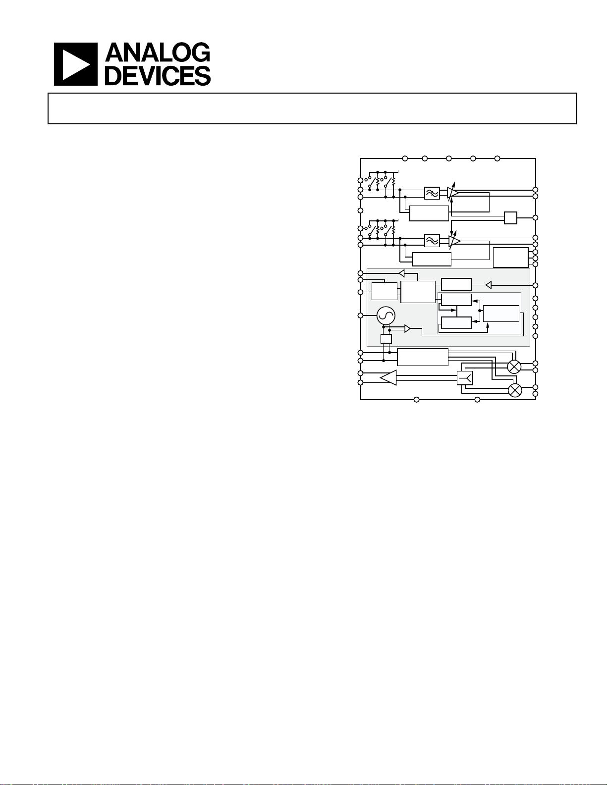
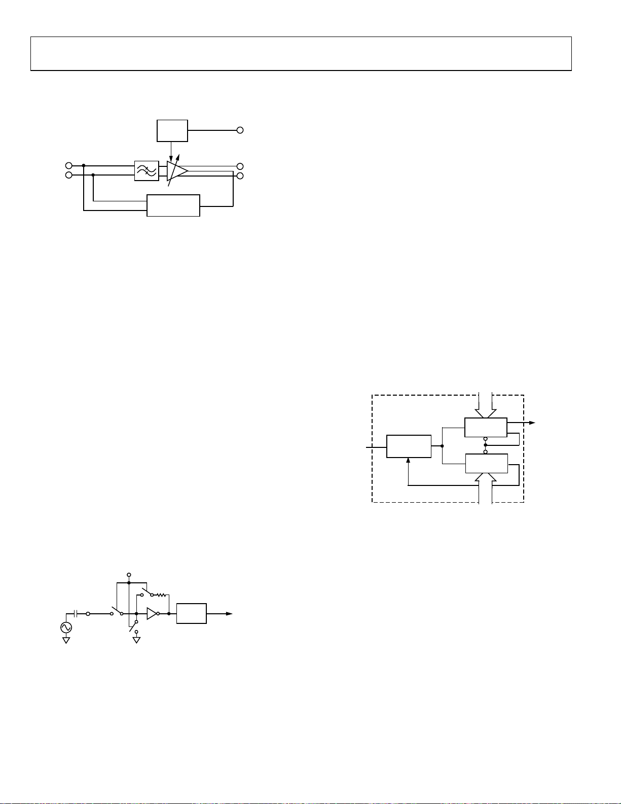
RxINIP
Rx
IN
Rx
Rx
IN
Rx
IN
MUXOUT
R
V
TUNE
LO
OUT
LO
OUT
Tx
OUT
Tx
OUT
Analog RF Front End
FUNCTIONAL BLOCK DIAGRAM
V
AV
QP
QN
SET
CP
RXV
DD
V
CM
IN
CM
CHARGE
PUMP
÷4
P
N
P
N
DC OFFSET
V
CORRECTI ON
CM
DC OFFSET
CORRECTI ON
PHASE
FREQUENCY
DETECTOR
QUADRATURE
PHASE SPLITTER
DD
P
R
COUNTER
B
COUNTER
A
COUNTER
Figure 1.
ADF9010
CE
DV
DD
ADF9010
INPUT SHIFT
REGISTE R
N COUNTER
N = BP + A
PRESCALER
P/P + 1
AGNDDGND
24-BIT
PLL
Rx
Rx
OVF
Rx
Rx
S
S
S
REF
C
C
C
C
C
Tx
Tx
Tx
Tx
BB
BB
BB
BB
CLK
DATA
LE
EXT
EXT
EXT
EXT
T
BB
BB
BB
BB
IP
IN
QP
QN
IN
1
2
3
4
IP
IN
QP
QN
07373-001
GENERAL DESCRIPTION
The ADF9010 is a fully integrated RF Tx modulator and Rx
analog baseband front end that operates in the frequency
range from 840 MHz to 960 MHz. The receive path consists
of a fully differential I/Q baseband PGA, low-pass filter, and
general signal conditioning before connecting to an Rx ADC
for baseband conversion. The Rx LPF gain ranges from 3 dB
to 24 dB, programmable in 3 dB steps. The Rx LPF features
four programmable modes with cutoff frequencies of 330 kHz,
880 kHz, and 1.76 MHz, or the filter can be bypassed if necessary.
Rev. 0
Information furnished by Analog Devices is believed to be accurate and reliable. However, no
responsibility is assumed by Analog Devices for its use, nor for any infringements of patents or other
rights of third parties that may result from its use. Specifications subject to change without notice. No
license is granted by implication or otherwise under any patent or patent rights of Analog Devices.
Trademarks and registered trademarks are the property of their respective owners.
The transmit path consists of a fully integrated differential Tx
direct I/Q upconverter with a high linearity PA driver amplifier.
It converts a baseband I/Q signal to an RF carrier-based signal
between 840 MHz and 960 MHz. The highly linear transmit
signal path ensures low output distortion.
Complete local oscillator (LO) signal generation is integrated
on chip, including the integer-N synthesizer and VCO, which
generate the required I and Q signals for transmit I/Q upconversion. The LO signal is also available at the output to drive an
external RF demodulator. Control of all the on-chip registers
is via a simple 3-wire serial interface. The device operates with a
power supply ranging from 3.15 V to 3.45 V and can be powered
down when not in use.
One Technology Way, P.O. Box 9106, Norwood, MA 02062-9106, U.S.A.
Tel: 781.329.4700 www.analog.com
Fax: 781.461.3113 ©2008 Analog Devices, Inc. All rights reserved.
Page 2

ADF9010
TABLE OF CONTENTS
Features .............................................................................................. 1
Applications ....................................................................................... 1
Functional Block Diagram .............................................................. 1
General Description ......................................................................... 1
Revision History ............................................................................... 2
Specifications ..................................................................................... 3
Transmit Characteristics .............................................................. 3
Receive Baseband Characteristics .............................................. 4
Integer-N PLL and VCO Characteristics .................................. 5
Write Timing Characteristics ...................................................... 6
Absolute Maximum Ratings ............................................................ 7
Transistor Count ........................................................................... 7
ESD Caution .................................................................................. 7
Pin Configuration and Function Descriptions ............................. 8
Typical Performance Characteristics ........................................... 10
Circuit Description ......................................................................... 12
Rx Section .................................................................................... 12
LO Section ................................................................................... 12
R Counter .................................................................................... 12
A and B Counters ....................................................................... 12
Tx Section .................................................................................... 14
Interfacing ................................................................................... 14
Latch Structure ........................................................................... 15
Control Latch .............................................................................. 21
Tx Latch ....................................................................................... 21
Rx Calibration Latch .................................................................. 21
LO Latch ...................................................................................... 22
Rx Latch ....................................................................................... 22
Initialization ................................................................................ 22
Interfacing ................................................................................... 22
Applications Information .............................................................. 23
Demodulator Connection ......................................................... 23
LO and Tx Output Matching .................................................... 24
PCB Design Guidelines ............................................................. 24
Outline Dimensions ....................................................................... 25
Ordering Guide .......................................................................... 25
REVISION HISTORY
8/08—Revision 0: Initial Version
Rev. 0 | Page 2 of 28
Page 3

ADF9010
SPECIFICATIONS
TRANSMIT CHARACTERISTICS
AVDD = DVDD = 3.3 V ± 5%, AGND = DGND = GND = 0 V, TA = 25°C, dBm refers to 50 Ω, 1.4 V p-p differential sine waves in
quadrature on a 500 mV dc bias, baseband frequency = 1 MHz, unless otherwise noted.
Table 1.
B Version
Parameter
1
Unit Test Conditions/Comments Min Typ Max
TRANSMIT MODULATOR CHARACTERISTICS
Operating Frequency Range 840 960 MHz
Range over which uncompensated sideband
suppression < −30 dBc
Output Power 3 dBm VIQ = 1.4 V p-p differential
Output P1 dB 10 dBm
Carrier Feedthrough −40 dBm
Sideband Suppression −46 dBc
Output IP3 24 dBm
= −4 dBm per tone, 10 MHz and 12 MHz
P
OUT
baseband input frequencies used.
Noise Floor −158 dBm/Hz
TRANSMIT BASEBAND CHARACTERISTICS
Input Impedance of Each Pin 4 kΩ typ Single-ended frequencies up to 2 MHz
Input Capacitance of Each Pin 3 pF At 10 MHz
Input Signal Level 1.4 V p-p Measured differentially at I or Q
Common-Mode Output Level 0.6 V
Tx Baseband 3 dB Bandwidth 20 MHz
POWER SUPPLIES
Voltage Supply 3.15 3.45 V
IDD
Digital IDD 5 6 mA
Rx Baseband 70 80 mA Maximum gain settings
Tx Modulator 140 mA Full power, baseband inputs biased at 0.5 V
LO Synthesizer and VCO 140 mA + 5 dBm LO power setting selected
Tot al IDD 360 410 mA
Power-Down
Rx VDD 1 mA
AVDD 1 20 μA
DVDD 1 20 μA
LOGIC INPUTS (SERIAL INTERFACE)
Input High Voltage, V
Input Low Voltage, V
Input Current, I
INH/IINL
1.4 V 1.8 V logic compatible
INH
0.4 V
INL
±1 μA
Input Capacitance, CIN 5 pF
LOGIC OUTPUTS (MUXOUT)
Output High Voltage, VOH DVDD − 0.4 V IOL = 500 μA
Output Low Voltage, VOL 0.4 V IOH = 500 μA
1
Operating temperature range for the B version is −40°C to +85°C.
Rev. 0 | Page 3 of 28
Page 4

ADF9010
RECEIVE BASEBAND CHARACTERISTICS
AVDD = DVDD = 3.3 V ± 5%, AGND = DGND = GND = 0 V, TA = 25°C, dBm refers to 50 Ω, 1.4 V p-p differential sine waves in
quadrature on a 500 mV dc bias, baseband frequency = 1 MHz, unless otherwise noted.
Table 2.
B Version
Parameter
RECEIVE BASEBAND PGA
Highest Voltage Gain 24 dB
Lowest Voltage Gain 3 dB
Gain Control Range 18 dB Programmable using 3-bit interface
Gain Control Step 3 dB
Noise Spectral Density (Referred to Input) 3.5 nV/√Hz At maximum PGA gain
RECEIVE BASEBAND FILTERS
3 dB Cutoff Frequency (Mode 0) 320 kHz After filter calibration
Gain Flatness 0.5 dB Typical from dc to 90 kHz
Differential Group Delay 500 μs DC to 360 kHz
150 μs 170 kHz to 310 kHz
Attenuation Template After filter calibration
@ 330 kHz Offset −3 dB
@ 500 kHz Offset −8 dB
@ 1 MHz Offset −28 dB
3 dB Cutoff Frequency (Mode 1) 880 kHz After filter calibration
Gain Flatness 0.5 dB DC to 90 kHz
Differential Group Delay 500 μs DC to 360 kHz
150 μs 170 kHz to 310 kHz
Attenuation Template After filter calibration
@ 880 kHz Offset −3 dB
@ 2 MHz Offset −17 dB
@ 4 MHz Offset −38 dB
3 dB Cutoff Frequency (Mode 2) 1.76 MHz After filter calibration
Gain Flatness 0.5 dB DC to 90 kHz
Differential Group Delay 500 μs DC to 360 kHz
150 μs 170 kHz to 310 kHz
Attenuation Template After filter calibration
@ 1.76 MHz Offset −3 dB
@ 4 MHz Offset −18 dB
@ 8 MHz Offset −38 dB
@ 16 MHz Offset −60 dB
3 dB Cutoff Frequency (Mode 3) 4 MHz After filter calibration
Gain Flatness 0.5 dB DC to 90 kHz
Differential Group Delay 500 μs DC to 360 kHz
@ 2 MHz Offset −0.5 dB
@ 4 MHz Offset −2 dB
Input Impedance of Each Pin
@ 24 dB gain 250 Ω
@ 3 dB gain 4 kΩ
Input Capacitance of Each Pin 3 pF At 10 MHz
Input Signal Level 2 V p-p Measured differentially at I or Q
Common-Mode Output Level 1.65 V On Rx baseband outputs
Maximum Residual DC 150 mV Baseband gain 0 dB − 27 dB
1
Operating temperature range for the B version is −40°C to +85°C.
1
Unit Test Conditions/Comments Min Typ Max
Rev. 0 | Page 4 of 28
Page 5

ADF9010
INTEGER-N PLL AND VCO CHARACTERISTICS
Table 3.
B Version
Parameter
1
Unit Test Conditions/Comments Min Typ Max
VCOOPERATING FREQUENCY 3360 3840 MHz
LO OUTPUT CHARACTERISTICS Measured at LO output (900 MHz)
VCO Control Voltage Sensitivity 8 MHz/V
3.6 GHz VCO frequency (taking into account
divide by 4)
Harmonic Content (Second) −27 dBc
Harmonic Content (Third) −14 dBc
Frequency Pushing (Open Loop) 1.2 MHz/V
Frequency Pulling (Open Loop) 10 Hz Into 2.00 VSWR load.
Lock Time 1000 μs 10 kHz loop bandwidth
Output Power −4 to +5 dBm
LO outputs combined in a 1:1 transformer;
programmable in 3 dB steps
Output Power Variation ±3 dB
NOISE CHARACTERISTICS Measured at LO output (900 MHz)
VCO Phase Noise Performance
2
@ 100 kHz Offset −120 dBc/Hz
@ 1 MHz Offset −141 dBc/Hz
@ 10 MHz Offset −154 dBc/Hz
In-Band Phase Noise
Normalized In-Band Phase Noise Floor
Spurious Frequencies at Output Channel Spacing −70 dBc
3, 4
−96 dBc/Hz @ 1 kHz offset from carrier
3, 4
−220 dBc/Hz
900 MHz offset, 1 MHz PFD frequency, 250 kHz
channel spacing; loop bandwidth = 7.5 kHz
PHASE DETECTOR
Phase Detector Frequency5 8 MHz
Maximum Allowable Prescaler Output Frequency
6
325 MHz
CHARGE PUMP
ICP Sink/Source With R
= 4.7 kΩ
SET
High Value 5 mA
Low Value 0.625 mA
R
Range 2.7 10 kΩ
SET
ICP Three-State Leakage Current 0.2 nA
Sink and Source Current Matching 2 % 1.25 V ≤ VCP ≤ 2.5 V
ICP vs. VCP 1.5 % 1.25 V ≤ VCP ≤ 2.5 V
ICP vs. Temperature 2 % VCP = 2.0 V
PLL REFERENCE
Reference Clock Frequency 10 104 MHz
Reference Clock Sensitivity 0.7 PLL VDD V p-p
Reference Input Capacitance 5 pF
REFIN Input Current ±100 μA
1
Operating temperature range for the B version is −40°C to +85°C.
2
The noise of the VCO is measured in open-loop conditions.
3
The phase noise is measured with the EVAL-ADF9010EBZ1 evaluation board and the Agilent E5052A spectrum analyzer. The spectrum analyzer provides the REFIN for
the synthesizer; offset frequency = 1 kHz.
4
f
= 10 MHz; f
REFIN
5
Guaranteed by design. Sample tested to ensure compliance.
6
This is the maximum operating frequency of the CMOS counters. The prescaler value should be chosen to ensure that the RF input is divided down to a frequency that
is less than this value.
= 1000 kHz; N = 3600; loop BW = 25 kHz.
PFD
Rev. 0 | Page 5 of 28
Page 6
ADF9010
WRITE TIMING CHARACTERISTICS
AVDD = DVDD = 3.3 V ± 5%; AGND = DGND = GND = 0 V; TA = 25°C, guaranteed by design, but not production tested.
Table 4.
Parameter Limit at t
t1 10 ns min S
t2 10 ns min S
t3 25 ns min S
t4 25 ns min S
t5 10 ns min S
t6 20 ns min SLE pulse width
S
CLCK
MIN
to t
(B Version) Unit Test Conditions/Comments
MAX
to S
DATA
DATA
CLK
CLK
CLK
t
t
3
4
t
t
2
1
setup time
CLK
to S
hold time
CLK
high duration
low duration
to SLE setup time
S
DATA
S
S
DB22DB23 (MSB)
LE
LE
DB2
DB1
(CONTROL BIT C2)
t
5
DB0 (LSB)
(CONTROL BIT C1)
t
6
7373-002
Figure 2. Write Timing Diagram
Rev. 0 | Page 6 of 28
Page 7
ADF9010
ABSOLUTE MAXIMUM RATINGS
TA = 25°C unless otherwise noted.
Table 5.
Parameter Rating
DVDD, RxVDD , AVDD to GND1 −0.3 V to +3.9 V
RxVDD, AVDD to DVDD −0.3 V to +0.3 V
VP to GND1 −0.3 V to +5.5 V
Digital I/O Voltage to GND1 −0.3 V to VDD + 0.3 V
Analog I/O Voltage to GND1 −0.3 V to AVDD + 0.3 V
Charge Pump Voltage to GND1 −0.3 V to VP to GND1
REFIN, LO
LO
EXT
Operating Temperature Range
Industrial (B Version) −40°C to +85°C
Storage Temperature Range −65°C to +150°C
Maximum Junction Temperature 150°C
LCSP θJA Thermal Impedance 26°C/W
Reflow Soldering
Peak Temperature 260°C/W
Time at Peak Temperature 40 sec
1
GND = AGND = DGND = 0 V.
EXT
P to LO
P, L O
N to GND1 −0.3 V to VDD + 0.3 V
EXT
N ±320 mV
EXT
Stresses above those listed under Absolute Maximum Ratings
may cause permanent damage to the device. This is a stress
rating only; functional operation of the device at these or any
other conditions above those indicated in the operational
section of this specification is not implied. Exposure to absolute
maximum rating conditions for extended periods may affect
device reliability.
This device is a high-performance RF integrated circuit with an
ESD rating of <0.5 kV and is ESD sensitive. Proper precautions
should be taken for handling and assembly.
TRANSISTOR COUNT
The ADF9010 transistor count is 40,454 (CMOS) and 994
(bipolar).
ESD CAUTION
Rev. 0 | Page 7 of 28
Page 8

ADF9010
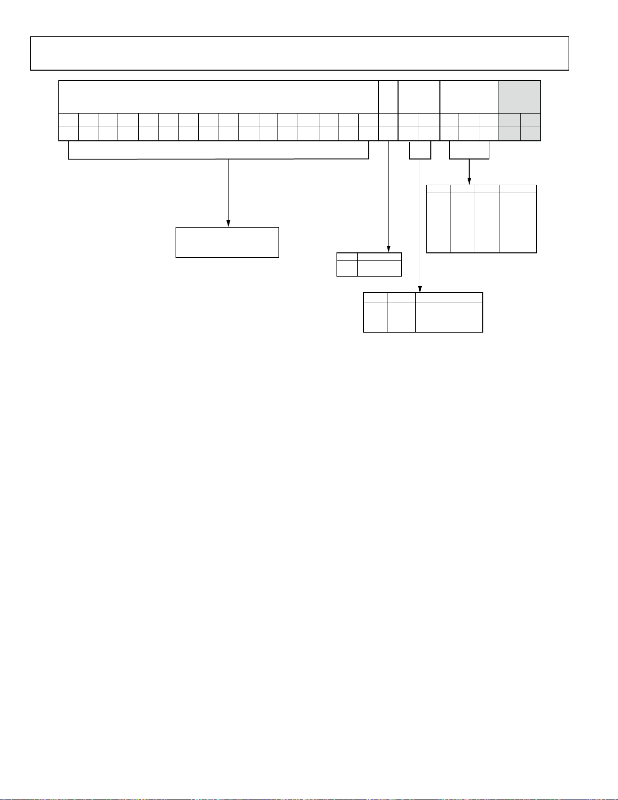
PIN CONFIGURATION AND FUNCTION DESCRIPTIONS
QN
QP
LO
LO
Rx
IN
Rx
IN
RxV
OUT
OUT
AGND
DGND
REF
DV
CP
AGND
DD
IN
IN
Rx
RxV
NC
AGND
OVF
MUXOUT
Rx
4847464544434241403938
1
IP
2
IN
3
DD
4
N
5
P
6
7
8
IN
9
DD
10
V
P
11
12
PIN 1
INDICATOR
ADF9010
TOP VIEW
(Not to Scale)
SLES
DATASCLK
CE
DV
37
DD
Rx
IN36
BB
Rx
35
IP
BB
34
Rx
QP
BB
33
Rx
QN
BB
32
C
3
EXT
31
C
4
EXT
30
R
SET
29
AV
DD
28
TxBBIN
27
Tx
IP
BB
26
Tx
QP
BB
25
Tx
QN
BB
NC = NO CONNECT
13141516171819
T
1
2
DD
C
EXT
EXT
AV
C
C
V
TUNE
2021222324
P
N
EXT
AGND
LO
LO
P
N
DD
EXT
AV
AGND
XOUT
XOUT
T
T
07373-004
Figure 3. Pin Configuration
Table 6. Pin Function Descriptions
Pin No. Mnemonic Description
1, 2 RxINIP, RxININ Input/Complementary In-Phase Input to the Receive Filter Stage.
3, 46 RxVDD
Receiver Filter Power Supply. This voltage ranges from 3.15 V to 3.45 V. Decoupling capacitors to the
analog ground plane should be placed as close as possible to this pin. RxV
4, 5 LO
OUT
N, LO
OUT
value as AV
P
Buffered Local Oscillator Output. These outputs are used to provide the LO for the external RF
and DVDD.
DD
demodulator. These require an RF choke to AVDD and a dc bypass capacitor before connection to a
demodulator.
6, 12, 18, 24, 44 AGND Analog Ground. This is the ground return path of analog circuitry.
7 DGND Digital Ground.
8 REFIN
PLL Reference Input. This is a CMOS input with a nominal threshold of V
input resistance of 100 kΩ (see Figure 13). This input can be driven from a TTL or CMOS crystal
oscillator, or it should be ac-coupled.
9, 37 DVDD
10 VP
11 CP
Digital Power Supply. This voltage ranges from 3.15 V to 3.45 V. Decoupling capacitors to the digital
ground plane should be placed as close as possible to this pin. DV
DD
This pin supplies the voltage to the charge pump. If the internal VCO is used, it should equal AV
and DV
Charge Pump Output. When enabled, this pin provides ±I
. If an external VCO is used, the voltage can be AVDD < VP < 5.5 V.
DD
to the external loop filter, which in turn
CP
drives the external VCO.
13 CT
A capacitor connected to this pin is used to roll off noise from the VCO. It should be decoupled to
AGND with a value of 10 nF. The output voltage on this part is proportional to temperature. At
ambient temperature, the voltage is 2.0 V.
14 C
EXT
1
A capacitor connected to this pin is used to roll off noise from the VCO. It should be decoupled to
AGND with a value of 10 nF.
15 C
EXT
2
A capacitor connected to this pin is used to roll off noise from the VCO. It should be decoupled to
AGND with a value of 10 nF.
16, 21, 29 AVDD
Analog Power Supply. This voltage ranges from 3.15 V to 3.45 V. Decoupling capacitors to the
analog ground plane should be placed as close as possible to this pin. AV
as DV
.
DD
must be the same
DD
/2 and a dc equivalent
DD
must be the same value as AVDD.
must be the same value
DD
DD
Rev. 0 | Page 8 of 28
Page 9

ADF9010
Pin No. Mnemonic Description
17 V
19, 20 LO
22, 23 Tx
25, 26 TxBBQN, TxBBQP Baseband Quadrature Phase Input/Complementary Input to the Transmit Modulator.
27, 28 TxBBIP, TxBBIN Baseband In-Phase Input/Complementary to the Transmit Modulator.
30 R
31 C
32 C
33, 34 RxBBQN, RxBBQP
35, 36 RxBBIP, RxBBIN
38 CE
39 S
40 S
41 SLE
42 MUXOUT
43 OVF
45 NC No Connect.
47, 48 RxINQP, RxINQN Input/Complementary Quadrature Input to the Receive Filter Stage.
TUNE
OUT
SET
EXT
EXT
CLK
DATA
EXT
4
3
P, L O
P, Tx
OUT
EXT
Control Input to the VCO. This input determines the VCO frequency and is derived from filtering the
CP output.
N
N
Single-Ended External VCO Input of 50 Ω. This is used if the ADF9010 utilizes an optional external VCO.
These pins are internally dc-biased and must be ac-coupled. AC-couple LO
and ac-couple the VCO signal with 100 pF through LO
EXT
P.
N to ground with 100 pF
EXT
Buffered Tx Output. These pins contain the Tx output signal, which can be combined in a balun for
best results.
Connecting a resistor between this pin and AGND sets the maximum charge pump output current.
The nominal voltage potential at the R
I
CPMAX
= 25.5/R
SET
pin is 0.66 V. The relationship between ICP and R
SET
SET
is
where:
is 5.1 kΩ.
R
SET
I
is 5 mA.
CPMAX
A capacitor connected to this pin is used to roll off noise from the VCO. It should be decoupled
to AGND with a value of 10 nF.
A capacitor connected to this pin is used to roll off noise from the VCO. It should be decoupled
to AGND with a value of 10 nF.
Output/Complementary Filtered Quadrature Signals from the Receive Filter Stage. The filtered
output is passed to the baseband MxFE chip.
Output/Complementary Filtered In-Phase from the Receive Filter Stage. The filtered output is
passed to the baseband MxFE chip.
Chip Enable. A Logic 0 on this pin powers down the device. A Logic 1 on this pin enables the device
depending on the status of the power-down bits.
Serial Clock Input. This serial clock is used to clock in the serial data to the registers. The data is
latched into the 24-bit shift register on the S
rising edge. This is a high impedance CMOS input.
CLK
Serial Data Input. The serial data is loaded MSB first with the two LSBs being the control bits. This is
a high impedance CMOS input.
Load Enable, CMOS Input. When LE goes high, the data stored in the shift register is loaded into
one of the four latches; the latch uses the control bits.
This multiplexer output allows either the PLL lock detect, the scaled VCO frequency, or the scaled
PLL reference frequency to be accessed externally.
A rising edge on this pin drops the gain of the Rx path by 6 dB. This is used to rapidly drop the gain
if the ADC detects an overload.
Rev. 0 | Page 9 of 28
Page 10
ADF9010
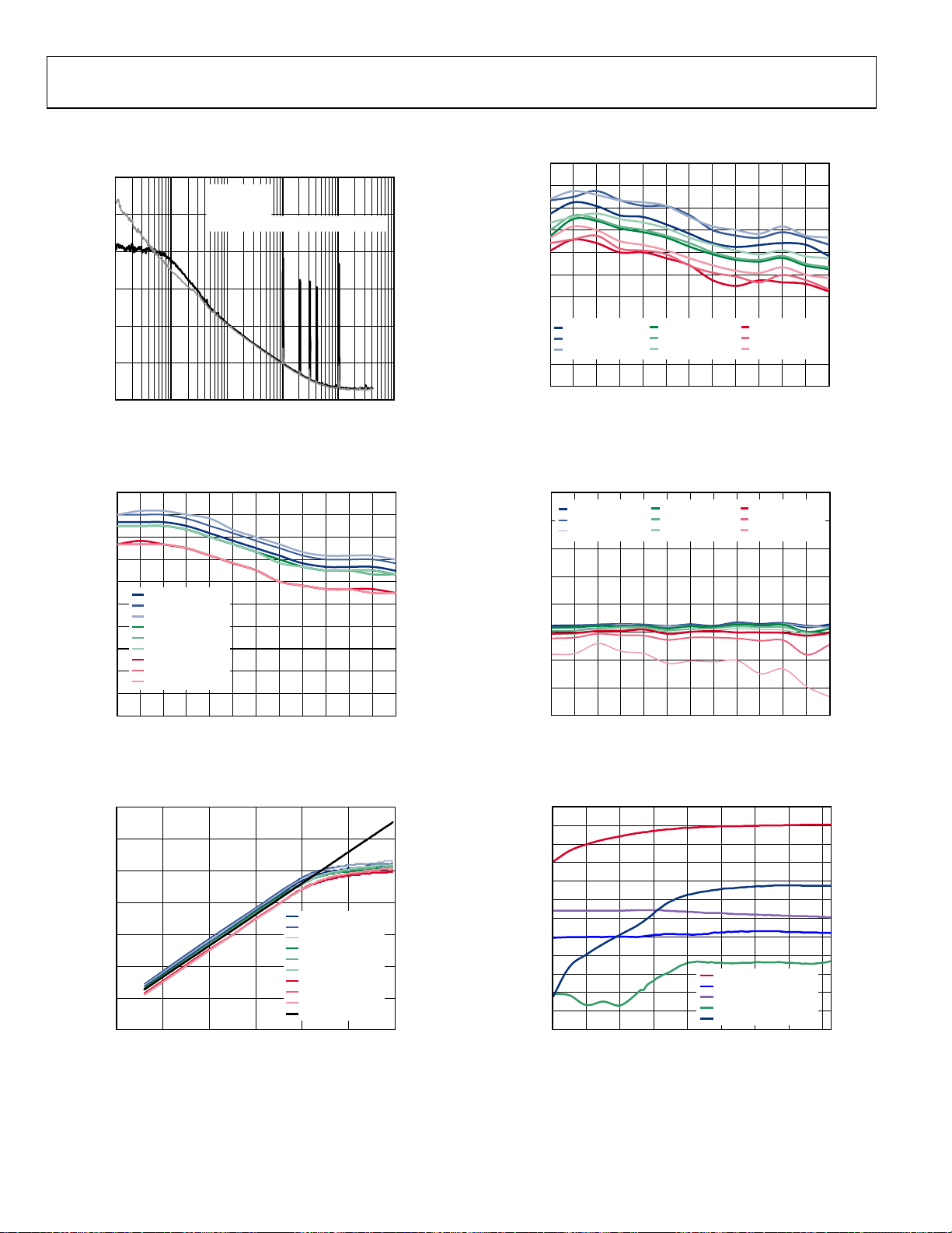
–
TYPICAL PERFORMANCE CHARACTERISTICS
40
–60
–80
–100
–120
PHASE NOISE (dBc/Hz)
–140
–160
1k
900MHz LO
10MHz REF
1MHz PFD
INTEGRATED PHASE ERRO R: 0.75 rms
FREQUENCY (Hz)
IN
100k 1M
10M
100M10k
Figure 4. LO Phase Noise (900 MHz, Including Open-Loop VCO Noise)
07373-013
28
27
26
25
24
23
OIP3 (dBm)
22
21
–40°C 3.15V OI P3
–40°C 3.3V OI P3
20
–40°C 3.45V OI P3
19
18
860 890 920870 900 930 940 950 960
840 850 880 910
+25°C 3.15V OIP3
+25°C 3.3V OIP3
+25°C 3.45V OIP3
LO FREQUE NCY (MHz)
+85°C 3.15V OIP3
+85°C 3.3V OIP3
+85°C 3.45V OIP3
07373-107
Figure 7. Output IP3 (dBm) vs. LO Frequency (Hz), with Supply and
Temperature Variations; Two-Tone Test (10 MHz and 12 MHz Baseband
Input Frequencies)
10
9
8
7
6
–40°C 3.15V P
5
–40°C 3.3V P
–40°C 3.45V P
4
+25°C 3.15V P
+25°C 3.3V P
3
Tx OUTPUT POWER (d Bm)
+25°C 3.45V P
+85°C 3.15V P
+85°C 3.3V P
2
+85°C 3.45V P
1
0
840 850 880 910
860 890 920870 900 930 940 950 960
OUT
OUT
OUT
OUT
OUT
OUT
OUT
OUT
OUT
LO FREQUENCY (MHz)
07373-105
Figure 5. Single Sideband Tx Power Output (dBm) vs. LO frequency (Hz) with
Supply and Temperature Variations; Outputs Combined in 50:100 Balun
20
15
10
5
(dBm)
0
OUT
P
–5
–10
–15
–10 –5 0 10 20
515
PIN (dBm)
–40°C 3.15V P
–40°C 3.3V P
–40°C 3.45V P
+25°C 3.15V P
+25°C 3.3V P
+25°C 3.45V P
+85°C 3.15V P
+85°C 3.3V P
+85°C 3.45V P
IDEAL
OUT
OUT
OUT
OUT
OUT
OUT
OUT
OUT
OUT
07373-106
Figure 6. Power Output vs. Baseband Input Power with Supply and
Temperature Variations
0
–40°C 3.15V SBS
–40°C 3.3V SBS
–10
–40°C 3.45V SBS
–20
–30
–40
–50
–60
SIDEBAND SUPRESSI ON (dBc)
–70
–80
840 850 880 910860 890 920870 900 930 940 950 960
+25°C 3.15V SBS
+25°C 3.3V SBS
+25°C 3.45V SBS
LO FREQUENCY (MHz)
+85°C 3.15V SBS
+85°C 3.3V SBS
+85°C 3.45V SBS
07373-108
Figure 8. Unwanted Sideband Suppression (dBc) vs. LO Frequency (Hz) with
Supply and Temperature Variations
20
10
0
–10
–20
–30
–40
–50
POWER (d Bc)
–60
–70
–80
–90
–100
0.2 1.0 1.8 2.6 3.4
DIFFERENTIAL INPUT VOLTAGE (V)
25°C 3.3V P
25°C 3.3V SBS (dBc)
25°C 3.3V LO FT (dBc)
25°C 3.3V HD2 (d Bm)
25°C 3.3V HD3 (d Bm)
OUT
(dBm)
3.00.6 1.4 2.2
07373-109
Figure 9. Second- and Third-Order Distortion, Sideband Suppression (dBc),
Carrier Feedthrough (dBm) and SBS P
vs. Baseband Differential Input
OUT
Level; LO Frequency = 900 MHz
Rev. 0 | Page 10 of 28
Page 11

ADF9010
9
8
7
6
5
4
3
Tx OUTPUT P OWER (dBm)
2
–40°C 3.15V P
–40°C 3.3V P
1
–40°C 3.45V P
0
1
+25°C 3.15V P
OUT
+25°C 3.3V P
OUT
+25°C 3.45V P
OUT
INPUT FREQ UENCY (MHz)
10
OUT
OUT
OUT
+85°C 3.15V P
+85°C 3.3V P
+85°C 3.45V P
OUT
OUT
OUT
Figure 10. Single Sideband Power vs. Baseband Input Frequency, with
Supply and Temperature Variations; Maximum Gain Setting Selected;
LO Frequency = 900 MHz
100
07373-110
20
0
–20
Fc 330KHz
–40
POWER (dB)
–60
–80
–100
10k
Fc 1MHz
Fc 2MHz
BYPASS
100k 1M
FREQUENCY (Hz)
Figure 11. Rx Filter Performance, Power vs. Input Frequency
10M
07373-111
Rev. 0 | Page 11 of 28
Page 12
ADF9010
CIRCUIT DESCRIPTION
Rx SECTION
PGA
SETTING
IP
Rx
IN
Rx
IN
IN
DC OFFSET
CORRECTION
Figure 12. Rx Filter
The Rx section of the ADF9010 features programmable baseband low-pass filters. These are used to amplify the desired Rx
signal from the demodulator while removing the unwanted
portion to ensure no antialiasing occurs in the Rx ADC.
These filters have a programmable gain stage, allowing gain to
be selected from 3 dB to 24 dB in steps of 3 dB. The bandwidth
of these filters is also programmable, allowing 3 dB cutoff frequencies of 330 kHz, 880 kHz, and 1.76 MHz, along with a
bypass mode. The filters utilize a fourth-order Bessel transfer
function (see the Specifications section for more information).
If desired, the filter stage can be bypassed.
Additionally, a rising edge on the OVF pin reduces the gain of
the Rx amplifiers by 6 dB. This is to correct a potential overflow
of the input to the ADC.
Updating the Rx calibration latch with the calibration bit
enabled calibrates the filter to remove any dc offset. The
3 dB cutoff frequency (f
) of the filters is calibrated also.
C
OVF
RxBBIP
Rx
BB
IN
07373-005
LO SECTION
LO Reference Input Section
The LO input stage is shown in Figure 13. SW1 and SW2
are normally closed switches; SW3 is normally open. When
power-down is initiated, SW3 is closed and SW1 and SW2 are
opened. This ensures that there is no loading of the REF
on power-down.
POWER-DOW N
CONTRO L
100kΩ
NC
SW1
NO
SW2
SW3
REF
IN
NC
Figure 13. Reference Input Stage
BUFFER
TO R COUNTER
IN
pin
7373-006
R COUNTER
The 14-bit R counter allows the input clock frequency to be
divided down to produce the input clock to the phase frequency
detector (PFD). Division ratios from 1 to 8191 are allowed.
A AND B COUNTERS
The A and B CMOS counters combine with the dual modulus
prescaler to allow a wide range of division ratios in the PLL
feedback counter. The counters are specified to work when
the prescaler output is 300 MHz or less.
Pulse Swallow Function
The A and B counters, in conjunction with the dual-modulus
prescaler (see Figure 14), make it possible to generate large
divider ratios. The equation for N is as follows:
N = BP + A
where:
N is the overall divider ratio of the signal from the external
RF input.
P is the preset modulus of the dual-modulus prescaler.
B is the preset divide ratio of the binary 13-bit counter (3 to 8191).
A is the preset divide ratio of the binary 5-bit swallow counter
(0 to 31).
N=BP+A
2
− P).
TO PFD
13-BIT B
COUNTER
FROM R F
INPUT STAGE
PRESCALER
P/P + 1
MODULUS
CONTROL
N DIVIDER
Figure 14. A and B Counters
LOAD
LOAD
6-BIT A
COUNTER
Prescaler (P/P + 1)
The dual-modulus prescaler (P/P + 1), along with the A and
B counters, enables the large division ratio, N, to be realized
(N = BP + A). The dual-modulus prescaler, operating at CML
levels, takes the clock from the RF input stage and divides it down
to a manageable frequency for the A and B CMOS counters.
The prescaler is programmable. The prescaler can be set in
software to 8/9, 16/17, or 32/33. For the ADF9010, however,
the 16/17 and 32/33 settings should be used. It is based on a
synchronous 4/5 core. A minimum divide ratio is possible for
fully contiguous output frequencies. This minimum is determined by P, the prescaler value, and is given by (P
07373-007
Rev. 0 | Page 12 of 28
Page 13
ADF9010
V
PFD and Charge Pump
The phase frequency detector (PFD) takes inputs from the
R counter and N counter (N = BP + A) and produces an output
proportional to the phase and frequency difference between
them (see Figure 15).
P
CHARGE
PUMP
U1
CLR1
CLR2
U2
UP
Q1D1
DELAY
DOWN
Q2D2
U3
CPGND
CP
HI
R DIVIDER
HI
N DIVIDER
RDIVIDER
DV
DD
ANALOG LO CK DETECT
DIGITAL LOCK DETECT
R COUNTER OUTP UT
N COUNTER OUTP UT
SDOUT
CONTRO LMUX
MUXOUT
DGND
Figure 16. MUXOUT Circuit
Voltage-Controlled Oscillator (VCO)
The VCO core in the ADF9010 uses 16 overlapping bands, as
shown in Figure 17, to allow a wide frequency range to be covered
with a low VCO sensitivity (K
) and to result in good phase noise
V
and spurious performance. The VCO operates at 4× the LO
frequency, providing an output range of 840 MHz to 960 MHz.
The correct band is chosen automatically by the band select
logic at power-up or whenever the LO latch is updated. During
band select, which takes five PFD cycles, the VCO V
TUNE
is
disconnected from the output of the loop filter and connected
to an internal reference voltage.
07373-114
NDIVIDER
CP OUTPUT
Figure 15. PFD Simplified Schematic and Timing (In Lock)
MUXOUT
The output multiplexer on the ADF9010 allows the user
to access various internal points on the chip. The state of
MUXOUT is controlled by M3, M2, and M1 in the control
latch. The full truth table is shown in Figure 22. Figure 16
shows the MUXOUT section in block diagram form.
Lock Detect
MUXOUT can be programmed for two types of lock detect:
digital and analog. Digital lock detect is active high. If the LDP
in the R counter latch is set to 0, digital lock detect is set high
when the phase error on three consecutive phase detector cycles
is less than 15 ns.
With the LDP set to 1, five consecutive cycles of less than 15 ns
phase error are required to set the lock detect. It stays set high
until a phase error of greater than 25 ns is detected on any
subsequent PD cycle.
The N-channel open-drain analog lock detect should be
operated with an external pull-up resistor of 10 kΩ nominal.
When a lock has been detected, this output is high with narrow
low-going pulses.
3.5
3.0
07373-008
2.5
2.
(V)
TUNE
1.5
V
1.0
0.5
0
750 800 850
SERIES 1
900 950 1000
FREQUENCY (Hz)
07373-020
Figure 17. VCO Bands
The R counter output is used as the clock for the band select logic
and should not exceed 1 MHz. A programmable divider is provided at the R counter input to allow division by 1, 2, 4, or 8 and
is controlled by Bit BSC1 and Bit BSC2 in the Tx latch. Where the
required PFD frequency exceeds 1 MHz, the divide ratio should be
set to allow enough time to select the correct band.
After the band is selected, normal PLL action resumes. The
nominal value of K
is 32 MHz/V or 8 MHz/V, taking into
V
account the divide by 4.
The output from the VCO is divided by 4 for the LO inputs to
the mixers, and for the LO output drive to the demodulator.
Rev. 0 | Page 13 of 28
Page 14

ADF9010
LO Output Mixers
The LO
P and LO
OUT
N pins are connected to the collectors
OUT
of an NPN differential pair driven by buffered outputs from the
VCO, as shown in Figure 18. To allow optimal power dissipation
vs. the output power requirements, the tail current of the differential pair is programmable via Bit TP1 and Bit TP2 in the
control latch. The four current levels that can be set are: 6 mA,
8.5 mA, 11.5 mA, and 17.5 mA. These levels give output power
levels of −4 dBm, −1 dBm, +2 dBm, and +5 dBm, respectively,
if both outputs are combined in a 1 + 1:1 transformer or a 180°
microstrip coupler.
If the outputs are used individually, the optimum output stage
consists of a shunt inductor to V
DD
.
Another feature of the ADF9010 is that the supply current to
the RF output stage is shut down until the part achieves lock as
measured by the digital lock detect circuitry. This is enabled by
the mute Tx until lock detect (F4) bit in the control latch.
VCO
BUFFER/
DIVIDE BY 4
LO
OUT
PLO
OUT
N
The ADF9010 has two double-balanced mixers, one for the
in-phase channel (I channel) and one for the quadrature
channel (Q channel). Both mixers are based on the Gilbert
cell design of four cross-connected transistors.
Tx Output
The Tx
P and Tx
OUT
N pins of the ADF9010 are connected
OUT
to the collectors of four NPN differential pairs driven by the
baseband signals, as shown in Figure 20. To allow the user
optimal power dissipation vs. the output power requirements,
the tail current of the differential pair is programmable via
Bit TP1 and Bit TP2 in the control latch. Two levels can be set;
these levels give output power levels of −3 dBm and, +3 dBm,
respectively, using a 50 Ω resistor to V
and ac coupling into a
DD
50 Ω load. Alternatively, both outputs can be combined in a 1 +
1:1 transformer or a 180° microstrip coupler. This buffer can be
powered off if desired.
Another feature of the ADF9010 is that the supply current to the Tx
output stage is shut down until the part achieves lock as measured
by the digital lock detect circuitry. This is enabled by the mute LO
until lock detect bit (F5) in the control latch.
Tx
P
OUT
N
Tx
OUT
07373-010
Figure 18. LO Output Section
Tx SECTION
VCO
LO
LO
LO
LO
EXT
EXT
OUT
OUT
P
N
TXBBIP
TXBBIN
Tx
P
OUT
Tx
N
OUT
QUAD
PHASE
SPLITTER
INT/
EXT
Tx
BB
Tx
BB
÷4
QP
QN
Figure 19. Tx Section
Tx Baseband Inputs
Differential in-phase (I) and quadrature baseband (Q) inputs
are high impedance inputs that must be dc-biased to approximately 500 mV dc and e driven from a low impedance source.
Nominal characterized ac signal swing is 700 mV p-p on each
pin. This results in a differential drive of 1.4 V p-p with a 500 mV
dc bias.
LO
LO
IP
IN
IP I N QP QN
LO
LO
QP
QN
07373-012
Figure 20. Tx Section
P
N
INTERFACING
Input Shift Register
The digital section of the ADF9010 includes a 24-bit input shift
register. Data is clocked into the 24-bit shift register on each
rising edge of S
. The data is clocked in MSB first. Data is
CLK
transferred from the shift register to one of four latches on
the rising edge of S
. The destination latch is determined by
LE
the state of the two control bits (C2, C1) in the shift register.
These are the two LSBs, DB1 and DB0, as shown in Figure 21.
07373-011
The truth table for Bit C3, Bit C2, and Bit C1 is shown in Tab le 7 .
It displays a summary of how the latches are programmed. Note
that some bits are used for factory testing and should not be
programmed by the user.
Table 7. Truth Table
Control Bits
Data Latch C3 C2 C1
X 0 0 Control latch
0 0 1 Tx latch
1 0 1 Rx calibration
X 1 0 LO latch
X 1 1 Rx filter
Rev. 0 | Page 14 of 28
Page 15

ADF9010
LATCH STRUCTURE
Figure 21 shows the three on-chip latches for the ADF9010. The two LSBs determine which latch is programmed.
CONTROL LATCH
MUTE
MUTE
LO
UNTIL
Tx LATCH
Tx
LO
LD
13-BIT REFERENCE COUNTER
UNTIL
LD
CP
F3F4
PD
STATE
THREE-
POLARITY
MUXOUT
RESET
COUNTER
R2R3R4R5R6R7R8R9R10R11R12R13
RESERVED
C3 (0) C2 (0) C 1 (1)
R1
CONTROL
BITS
C2 (0) C1 (0)RES RESF1M1M2F2PD4RES CPI1CPI2PD1PD2PD3 M3
CONTROL
BITS
RESERVED
LO PHASE
SELECT
P3
CPI3
BAND
SELECT
CLOCK
BSC1
CHARGE
PUMP
CURRENT
OUTPUT
POWER
P2 P1 F5
Tx
OUTPUT
PD PLL
PD Rx
DB21
DB22DB23
DB21DB22DB23
P2
PD VCO
DB20 DB19 DB18 DB17 DB16 DB15 DB14 DB13 DB12 DB11 DB10 DB9 DB8 DB7 DB6 DB5 DB4 DB3 DB2 DB1 DB0
Tx MOD
LO PHASE
SELECT
DB20 DB19 DB18 DB17 DB16 DB15 DB14 DB13 DB12 DB11 DB10 DB9 DB8 DB7 DB6 DB5 DB4 DB3 DB2 DB1 DB0
P1
POWER
PD Tx
TP1TP2
BSC2T1T2T3
Rx CALIBRATION
CP GAIN
LO PHASE
DB20 DB19 DB18 DB17 DB16 DB15 DB14 DB13 DB12 DB11 DB10 DB9 DB8 DB7 DB6 DB5 DB4 DB3DB21DB22DB23
N DIV
M1
Tx MOD
SELECT
MUX
T12T13
LO PHASE
SELECT
PRESCALER
P2 P1
G1
T15T16 T7
T14 HP
T11
BAND
SELECT
CLOCK
T10
CAL
Rx FILTER
R13BSC1BSC2T1T2T3P2 P1P3
TEST MODES
T8
T9
Rx CALIBRATION DIVIDER
LO LATCH
13-BIT B COUNTER
Rx LATCH
T6 T5 T4
Figure 21. Latch Summary
HIGH-PASS FILTER BOOST
TIMEOUT COUNTER
RC2RC3RC4RC5RC6
Rx FILTER
HPF
BANDWIDTH
BOOST
T3
T1
T2
BW2
HP2 HP1HP3HP4HP5HP6RC1
5-BIT A COUNTER
Rx FILTER
GAIN STEPS
BW1
G3
CONTROL
BITS
DB2 DB1 DB0
C3 (1)C2 (0)C1 (1)
CONTROL
DB2 DB1 DB0DB20 DB19 DB18 DB17 DB16 DB15 DB14 DB13 DB12 DB11 DB10 DB9 DB8 DB7 DB6 DB5 DB4 DB3DB21DB22DB23
C2 (1) C2 (0)A1A2A3A4A5B1B2B3B4B5B6B7B8B9B10B11B12B13
CONTROL
DB2 DB1 DB0DB20 DB19 DB18 DB17 DB16 DB15 DB14 DB13 DB12 DB11 DB10 DB9 DB8 DB7 DB6 DB5 DB4 DB3DB21DB22DB23
G1
C2 (1) C1 (1)
G2
BITS
BITS
07373-014
Rev. 0 | Page 15 of 28
Page 16

ADF9010
MUTE
LO
UNTIL
LD
MUTE
Tx
UNTIL
LD
CP
F3F4
STATE
THREE-
POLARITY
F1
0NORMAL
1 COUNTERS HELD
M3 M2 M1 OUTPUT
0 0 0 THREE- STATE OUTPUT
0 0 1 DIGITAL LOCK DETECT
0 1 0 N DI VIDER OUT PUT
011DV
1 0 0 R DI VIDER OUT PUT
1 0 1 N-CH ANNEL OPEN- DRAIN
1 1 0 SERI AL DATA OUTP UT
111DGND
COUNTER
COUNTER
OPERATIO N
IN RESET
RESET
MUXOUT
PD
RESERVED
THESE BITS ARE
RESERVED
AND SHOULD BE
SET TO 0, 1
(ACTIVE HI GH)
DD
LOCK DETECT
CONTROL
BITS
C2 (0) C 1 (0)RES RESF1M1M2F2PD4RES CPI1CPI2PD1PD2PD3 M3
RESERVED
DB22DB23
THIS BIT
IS RESERVED
FOR FACTORY
TESTING AND
SHOULD BE
SET TO 0
POWER DOWN
PD4
Rx
0 DISABLED
1 ENABLED
POWER DOWN
PD3
PLL
0DISABLED
1 ENABLED
CPI3
CHARGE
PUMP
CURRENT
Tx
OUTPUT
PD PLL
PD Rx
PD VCO
DB20 DB19 DB18 DB17 DB16 DB15 DB14 DB13 DB12 DB11 DB10 DB9 DB8 DB7 DB6 DB5 DB4 DB3 DB2 DB1 DB0
DB21
POWER
PD Tx
TP1TP2
LO
OUTPUT
POWER
P2 P1 F5
POWER DO WN
PD2
VCO
0DISABLED
1 ENABLED
POWER DOWN
PD1
Tx
0DISABLED
1 ENABLED
TP2 TP1
00
01
10
11
CPI3 CPI2 CPI1 2.7kΩ 4.7kΩ 10kΩ
0001.250.630.31
0012.501.250.63
0103.751.870.94
0115.002.501.25
1006.253.131.56
1017.503.751.87
1108.754.382.19
1 1 1 10.0 5.00 2.50
Tx OUTPUT POWER
FULLY ON
–6dB
–6dB
MUTE
ICP(mA)
Figure 22. Control Latch
PHASE DETECTOR
F2
POLARIT Y
0NEGATIVE
1 POSITIVE
CHARGE PUMP
F3
OUTPUT
0NORMAL
1 THREE-STATE
F4
0 DI SABLED
1 EN ABLED
F5
0 DI SABLED
1 EN ABLED
P2 P1 LO OUTPUT P OWER ( COMBI NED)
0 0 –4 dBm
0 1 –1 dBm
10+2 dBm
11+5 dBm
MUTE LO UNTIL
LOCK DETECT
MUTE Tx UNTIL
LOCK DETECT
07373-015
Rev. 0 | Page 16 of 28
Page 17

ADF9010
LO PHASE
SELECT
P2
P3
X = DON’T
CARE
Tx MOD
LO PHASE
SELECT
DB20 DB19 DB18 DB17 DB16 DB15 DB14 DB13 DB12 DB11 DB10 DB9 DB8 DB7 DB6 DB5 DB4 DB3 DB2 DB1 DB0DB21DB22DB23
P1
BAND
SELECT
CLOCK
BSC2T1T2T3
BSC1
R13 R12 R11 R3 R2 R1 DIVI DE RATIO
0 0 0 ..........
0 0 0 .......... 0 1 0 2
0 0 0 .......... 0 1 1 3
0 0 0 .......... 1 0 0 4
. . . .......... . . . .
. . . .......... . . . .
. . . .......... . . . .
1 1 1 .......... 1 0 0 8188
1 1 1 .......... 1 0 1
1 1 1 .......... 1 1 0 8190
1 1 1 .......... 1 1 1 8191
BSC2 BSC1 BAND SEL ECT CLOCK DI VIDER
0 0 NOT ALLOWED
0 1 NOT ALLOWED
1 0 NOT ALLOWED
118
THESE BITS ARE RESERVED AND SHOULD BE SET TO 1, 1
13-BIT REFERENCE COUNTER
..........
0011
CONTROL
BITS
C3 (0) C2 (0) C1 (1)
R1
R2R3R4R5R6R7R8R9R10R11R12R13
8189
T3 T2 T1 OUTPUT
0 0 0 NORMAL QUADRATURE
0 0 1 I TO BOTH
0 1 0 Q TO BOTH
0 1 1 EXTERNAL LO, Q UADRATURE
1 X X ALL OFF
P3 P2 P1 OUTPUT
000I OUT
001Q OUT
010IB OUT
011QB OUT
1 0 0 EXTE RNAL I
1 0 1 EXTE RNAL Q
1 1 0 EXTERNAL I TO PLL, O UT OFF
1 1 1 ALL OFF
Figure 23. Tx Latch
07373-016
Rev. 0 | Page 17 of 28
Page 18

ADF9010
LO PHASE
SELECT
X = DON’T
CARE
Tx MOD
LO PHASE
SELECT
BAND
SELECT
CLOCK
Rx FILTER
Rx CALIBRATION DIVIDER
CAL
R13BSC1BSC2T1T2T3P2 P1P3
Rx FILTER f
F5
0DISABLED
1 ENABLED
BSC2 BSC1 BAND SELECT CLOCK D IVIDER
0 0 NOT ALLOW ED
0 1 NOT ALLOW ED
1 0 NOT ALLOW ED
118
THESE BITS ARE RESERVED AND SHOULD BE SET TO 1, 1
CALIBRATI ON
C
HIGH-PASS FILTER BOOST
TIMEOUT COUNTER
CONTROL
BITS
DB2 DB1 DB0DB20 DB19 DB18 DB17 DB16 DB15 DB14 DB13 DB12 DB11 DB10 DB9 DB8 DB7 DB6 DB5 DB4 DB3DB21DB22DB23
RC2RC3RC4RC5RC6
HP6 .......... HP2 HP1
0 .......... 0 0 0
0 .......... 0 1 1
0 .......... 1 0 2
0 .......... 1 1 3
. .......... . . .
. .......... . . .
. .......... . . .
1 .......... 0 0 60
1 .......... 0 1 61
1 .......... 1 0 62
1 .......... 1 1 63
HP2 HP1HP3HP4HP5HP6RC1
C3 (1) C2 (0) C1 (1)
TIMEOUT
COUNTER
CYCLES
T3 T2 T1 OUTPUT
0 0 0 NORMALQUADRATURE
0 0 1 I TO BOTH
0 1 0 Q TO BOTH
0 1 1 EXTERNAL LO, QU ADRATURE
1 X X ALL OFF
P3 P2 P1 OUTPUT
000I OUT
001Q OUT
010IB OUT
011QB OUT
1 X X ALL OFF
RC6 .......... RC2 RC1
0 .......... 0 0 0
0 .......... 0 1 1
0 .......... 1 0 2
0 .......... 1 1 3
. .......... . . .
. .......... . . .
. .......... . . .
1 .......... 0 0 60
1 .......... 0 1 61
1 .......... 1 0 62
1 .......... 1 1 63
Figure 24. Rx Calibration Latch
CAL COUNTER
DIVIDE RAT IO
07373-017
Rev. 0 | Page 18 of 28
Page 19

ADF9010
PRESCALER
MUX
N DIV
CP GAIN
G1P2 P1
M1
X = DON’T CARE
N DIV MUX O PERATIO N
0 VCO FEEDBACK TO N DI VIDER.
1 MUX FEEDBACK TO N DIVI DER.
0 0 0 .......... 0 0 0 NOT ALLOWED
0 0 0 .......... 0 0 1 NOT ALLOWED
0 0 0 .......... 0 1 0 NOT ALLOWED
0 0 0 .......... 0 1 1 3
. . . .......... . . . .
. . . .......... . . . .
. . . .......... . . . .
1 1 1 .......... 1 0 0 8188
1 1 1 .......... 1 0 1 8189
1 1 1 .......... 1 1 0 8190
1 1 1 .......... 1 1 1 8191
B12B12 B11 B3 B2 B 1 B COUNTER DIV IDE RATIO
13-BIT B COUNTER
5-BIT A COUNTER
DB2 DB1 DB0DB20 DB19 DB18 DB17 DB16 DB15 DB14 DB13 DB12 DB11 DB10 DB9 DB8 DB7 DB6 DB5 DB4 DB3DB21DB22DB23
A5 .......... A2 A1
0 .......... 0 0 0
0 .......... 0 1 1
0 .......... 1 0 2
0 .......... 1 1 3
. .......... . . .
. .......... . . .
. .......... . . .
1 .......... 0 0 28
1 .......... 0 1 29
1 .......... 1 0 30
1 .......... 1 1 31
CONTROL
BITS
C2 (1) C2 (0)A1A2A3A4A5B1B2B3B4B5B6B7B8B9B10B11B12B13
A COUNTER
DIVIDE RAT IO
CP GAIN OPERATION
0 USE THE PROG RAMMED CHARGE PUMP
CURRENT SETTI NG FROM CONTRO L REGI STER
1 USE THE M AXIMUM CHARGE PUM P CURRENT
SETTING
P2 P1 PRESCALER VALUE
008/9
0116/17
1032/33
1132/33
Figure 25. LO Latch
Rev. 0 | Page 19 of 28
N = BP + A, P I S THE PRESCALER VALUE SET IN THE FUNCTION LATCH.
B MUST BE G REATER THAN OR EQUAL TO A. FOR CO NTINUOUSLY
ADJACENT VALUES OF (N × F
) AT THE OUTPUT, N
REF
IS (P2– P).
MIN
7373-018
Page 20
ADF9010
DB2 DB1 DB0DB20 DB19 DB18 DB17 DB16 DB15 DB14 DB13 DB12 DB11 DB10 DB9 DB8 DB7 DB6 DB5 DB4 DB3DB21DB22DB23
G1T9
CONTROL
BITS
C2 (1) C1 (1)
07373-019
TEST MODES
T10T1 1 T6 T5 T4 T2T3
THESE BITS ARE USED FOR FACT ORY
TESTING AND SHOULD NO T BE
PROGRAMMED BY THE USER.
THEY SHOULD BE SET TO 0.
Rx FILTER
HPF
BANDWIDTH
BOOST
BW1
HP HPF BO OST
0 DISABLED
1 ENABLED
BW2 BW1 Rx FI LTER BANDWI DTH
00 LOW
01 1MHz
10 2MHz
1 1 BYPASSED
Rx FILTER
GAIN STEPS
G2G3BW2T1T15T16 T7T8T12T13T14 HP
G3 G2 G1 FILTER GAIN
0003dB
0016dB
0109dB
0 1 1 12dB
1 0 0 15dB
1 0 1 18dB
1 1 0 21dB
1 1 1 24dB
Figure 26. Rx Latch
Rev. 0 | Page 20 of 28
Page 21

ADF9010
CONTROL LATCH
With (C2, C1) = (0, 0), the control latch is programmed.
Figure 22 shows the input data format for programming
the control latch.
Power-Down
Programming a 1 to PD4, PD3, PD2, PD1 powers down
the circuitry for the Rx filters, PLL, VCO, and Tx sections,
respectively. Programming a 0 enables normal operation for
each section.
Tx Output Power
Bit TP1 and Bit TP2 set the output power level of the VCO.
See the truth table in Figure 22.
Charge Pump Current
Bit CPI3, Bit CPI2, and Bit CPI1 determine Current Setting 2.
See the truth table in Figure 22.
LO Output Power
Bit P1 and Bit P2 set the output power level of the LO. See the
truth table in Figure 22.
Mute LO Until Lock Detect
Bit F5 is the mute until lock detect bit. This function, when
enabled, ensures that the LO outputs are not switched on
until the PLL is locked.
Mute Tx Until Lock Detect
Bit F4 is the mute Tx until lock detect bit. This function, when
enabled, ensures that the Tx outputs are not switched on until
the PLL is locked.
Charge Pump Three-State
Bit F3 puts the charge pump into three-state mode when programmed to a 1. It should be set to 0 for normal operation.
Phase Detector Polarity
Bit F2 sets the phase detector polarity. The positive setting
enabled by programming a 1 is used when using the on-chip
VCO with a passive loop filter or with an active noninverting
filter. It can also be set to 0. This is required if an active inverting
loop filter is used.
MUXOUT Control
The on-chip multiplexer is controlled by M3, M2, and M1.
See the truth table in Figure 22.
Counter Reset
Bit F1 is the counter reset bit for the PLL of the ADF9010.
When this bit is set to 1, the R, A, and B counters are held
in reset. For normal operation, this bit should be 0.
Reserved Bits
DB3 and DB2 are spare bits that are reserved. They should
be programmed to 0 and 1, respectively.
Tx LATCH
With (C3, C2, C1) = (0, 0, 1), the Tx latch is programmed.
Figure 23 shows the input data format for programming
the Tx latch.
LO Phase Select
Bit P3, Bit P2, and Bit P1 set the phase of the LO output to the
demodulator. This enables the user to select the phase delay of
the Rx LO signal to the demodulator in 90° steps. See the truth
table in Figure 23. The Rx LO output can be disabled if desired.
Tx Modulation LO Phase Select
Bit T3, Bit T2, and Bit T1 set the input modulation of the
VCO. Normal quadrature to each mixer can be replaced by
choosing one LO phase to both mixers if desired. The normal
(I) or quadrature (Q) phase can be chosen. See the truth table
in Figure 23.
Band Select Clock
Bits BSC2 and Bit BSC1 set a divider for the band select logic
clock input. The recommended setting is 1, 1, which programs
a value of 8 to the divider. No other setting is allowed.
Reference Counter
R13 to R1 set the counter divide ratio. The divide range is 1
(00 … 001) to 8191 (111 … 111).
Rx CALIBRATION LATCH
With (C3, C2, C1) = (1, 0, 1), the Rx calibration latch is
programmed. Figure 24 shows the input data format for
programming the Rx calibration latch.
LO Phase Select
Bit P3, Bit P2, and Bit P1 set the phase of the LO output to the
demodulator. This enables the user to select the phase delay of
the Rx LO signal to the demodulator in 90° steps. See the truth
table in Figure 24. The Rx LO output can be disabled if desired.
Tx Modulation LO Phase Select
Bit T3, Bit T2, and Bit T1 set the input modulation of the VCO.
Normal quadrature to each mixer can be replaced by choosing
one LO phase to both mixers if desired. The normal (I) or quadrature (Q) phase can be chosen. See the truth table in Figure 24.
Band Select Clock
Bit BSC2 and Bit BSC1 set a divider for the band select logic
clock input. The recommended setting is 1, 1, which programs
a value of 8 to the divider. No other setting is allowed.
Rx Filter Calibration
Setting Bit R13 high performs a calibration of the Rx filters’
cutoff frequency, f
frequency calibration sequence is not initiated if this latch is
programmed.
. Setting this bit to 0 ensures the filter cutoff
C
Rev. 0 | Page 21 of 28
Page 22

ADF9010
Rx Calibration Divider
Bit RC6 to Bit RC1 program a 6-bit divider, which outputs
a divided REF
frequency, f
signal to assist calibration of the cutoff
IN
, of the Rx filters. The calibration circuit uses
C
this divideddown PLL reference frequency to ensure an
accurate cutoff frequency in the Rx filter. The divider value
should be chosen to ensure that the frequency of the divided
down signal is exactly 2 MHz, that is, if a 32 MHz crystal is
used as the PLL REF
frequency, then a value of 16 should
IN
be programmed to the counter to ensure accurate calibration.
High-Pass Filter Boost Timeout Counter
In most applications of the ADF9010, a high-pass filter is placed
between the demodulator outputs and the ADF9010 Rx inputs.
The capacitors used in these filters may require a long charge
up time, and to address this, a filter boost function exists that
charges up the capacitor to ~1.6 V. The duration for this boost
is set by the product of the period of the Rx calibration signal,
(REF
divided by the Rx calibration divider) and the 6-bit value
IN
programmed to these registers. This value can be as large as 63.
Programming a value of 000000 leads to the calibration time
being manually set by the HPF boost in the Rx latch. It becomes
necessary in such cases to program this bit to 0 for normal Rx
operation.
LO LATCH
Program the LO latch with (C2, C1) = (1, 0). Figure 25 shows
the input data format for programming the LO latch.
Prescaler
Bit P2 and Bit P1 in the LO latch set the prescaler values.
CP Gain
Setting G1 to 0 chooses the programmed charge pump current
setting from the control latch. Setting this bit to 1 chooses the
maximum possible setting.
N Div Mux
Setting M1 to 0 feeds the VCO signals back to the N divider.
Setting this bit to 1 allows the mux signal to be fed back instead.
B Counter Latch
Bit B13 to Bit B1 program the B counter. The divide range is
3 (00 … 0011) to 8191 (11 … 111).
A Counter Latch
Bit A5 to Bit A1 program the 5-bit A counter. The divide range
is 0 (00000) to 31 (11111).
Rx LATCH
Program the Rx latch with (C2, C1) = (1, 1). Figure 26 shows
the input data format for programming the LO latch.
High-Pass Filter Boost
This function is enabled by setting the HP bit to 1. A 0 disables
this function. This is used to reduce settling time on the highpass filter from the Rx demodulator. This is usually used in
conjunction with the high-pass filter boost counter (See the
Rx Calibration Latch section).
Rx Filter Bandwidth
The Rx filter bandwidth is programmable and is controlled by
Bit BW2 and Bit BW1. See the truth table in Figure 26.
Rx Filter Gain Steps
Bit G3 to Bit G1 set the gain of the Rx filters. The gain can
vary from 3 dB to 24 dB in 3 dB steps. See the truth table in
Figure 26.
INITIALIZATION
The correct initialization sequence for the ADF9010 is as follows:
1. Power-down all blocks: Tx, Rx, PLL, and VCO. Set the Tx
output power off control latch to (1, 1). Set the LO phase
select off (P1, P2, P3) in Tx latch to (1, 1, 1).
2. Program the R1 latch with the desired R counter and
Tx values.
3. Program R5 with Rx calibration data for frequency
calibration and high-pass filter boost.
4. Program R0 to power up all LO and Tx/Rx blocks.
5. Program R2 to encode correct LO frequency.
6. Program R3 to power up Rx filter.
INTERFACING
The ADF9010 has a simple SPI®-compatible interface for
, S
writing to the device. S
CLK
transfer. See Figure 2 for the timing diagram.
The maximum allowable serial clock rate is 20 MHz. This
means that the maximum update rate possible for the device
is 833 kHz or one update every 1.2 μs. This is certainly more
than adequate for systems that have typical lock times in
hundreds of microseconds.
, and SLE control the data
DATA
Rev. 0 | Page 22 of 28
Page 23
ADF9010
APPLICATIONS INFORMATION
RXV
AV
DD
DD
V
CM
RxINIP
IN
Rx
IN
QP
Rx
IN
QN
Rx
IN
MUXOUT
R
SET
CHARGE
CP
PUMP
V
TUNE
ANTENNA SWIT CH MODULE
BALUN
LO
P
OUT
N
LO
PA MODULE
BALUN
OUT
Tx
P
OUT
N
Tx
OUT
V
CM
PHASE
FREQUENCY
DETECTOR
DC OFFSET
CORRECTI ON
DC OFFSET
CORRECTION
Figure 27. Applications Diagram
The diagram in Figure 27 shows the ADF9010 in an RFID application. The demodulator is driven by the LO
x pins of the
OUT
ADF9010. This demodulator produces quadrature baseband
signals that are gained up in the ADF9010 Rx filters. These
filtered analog baseband signals are then digitized by the ADC
on a mixed signal front-end (MxFE) part. The digital signals
are then processed by DSP.
On the transmit side, the MxFE generates quadrature analog
baseband signals, which are upconverted to RF using the integrated PLL and VCO. The modulated RF signals are combined
using a balun and gained up to 30 dBm by a power amplifier.
DEMODULATOR CONNECTION
To receive the back-scattered signals from an RFID tag,
the ADF9010 needs to be used with a high dynamic range
demodulator, such as the ADL5382 that is suitable for RFID
applications. Some extra filtration is provided by the optional
V
P
R
COUNTER
B
COUNTER
A
COUNTER
CE
DV
DD
AGNDDGND
ADF9010
INPUT SHIFT
REGISTER
N COUNTER
N = BP + A
PRESCALER
P/P + 1
24-BIT
PLL
Rx
Rx
Tx
Tx
Tx
Tx
Rx
Rx
OVF
S
S
S
REF
C
C
C
C
C
BB
BB
BB
BB
CLK
DATA
LE
EXT
EXT
EXT
EXT
T
BB
BB
BB
BB
QP
QN
IN
1
2
3
4
IP
IN
QP
QN
MxFE
SHA
IP
IN
SHA
ADC
AGC
Tx BASEBAND
Rx BASEBAND
DAC
DAC
AUX
DAC
DIGI TAL
CONTROL
24-BIT
INPUT SHIFT
REGISTER
AUX
AUX
DAC
DAC
shunt capacitors and series inductors. Due to the large selfblocker, a 100 nF capacitor removes the dc generated by the
self-blocker inherent to RFID systems. This system is used
on the EVAL-ADF9010EBZ1 evaluation board.
100nF
100nF
DEMOD
ADL5382
1.2nF
0Ω
47pF
0Ω
IHI
ILO
Figure 28. ADL5382 to ADF9010 Rx Interface
CLK
DATA
LE
EN
07373-003
R
x
IP
IN
ADF9010
x
IN
R
IN
07373-021
Rev. 0 | Page 23 of 28
Page 24

ADF9010
LO AND Tx OUTPUT MATCHING
The LO and Tx output stages are each connected to the collectors
of an NPN differential pair driven by buffered outputs from the
VCO or mixer outputs, respectively.
The recommended matching for each of these circuits consists
of a 7.5 nH shunt inductor to V
in the case of the Tx output a 50:100 balun to combine the Tx
outputs. The Anaren BD0810J50100A00 is ideally suited to this
task.
, a 100 pF series capacitor, and
DD
PCB DESIGN GUIDELINES
The lands on the chip scale package (CP-48-1) are rectangular.
The printed circuit board pad for these should be 0.1 mm
longer than the package land length and 0.05 mm wider than
the package land width. The land should be centered on the
pad. This ensures that the solder joint size is maximized. The
bottom of the chip scale package has a central thermal pad.
The thermal pad on the printed circuit board should be at least
as large as this exposed pad. On the printed circuit board, there
should be a clearance of at least 0.25 mm between the thermal
pad and the inner edges of the pad pattern. This ensures that
shorting is avoided.
Thermal vias can be used on the printed circuit board thermal
pad to improve thermal performance of the package. If vias are
used, they should be incorporated in the thermal pad at a 1.2 mm
pitch grid. The via diameter should be between 0.3 mm and
0.33 mm, and the via barrel should be plated with 1 oz. copper
to plug the via.
The user should connect the printed circuit board thermal pad
to AGND.
Rev. 0 | Page 24 of 28
Page 25

ADF9010
OUTLINE DIMENSIONS
0.30
0.23
0.18
PIN 1
48
INDICAT OR
1
BSC SQ
PIN 1
INDICATO R
7.00
0.60 MAX
37
36
0.60 MAX
1.00
0.85
0.80
12° MAX
SEATING
PLANE
(BOTTOM VIEW)
25
24
EXPOSED
PAD
5.50
REF
TOP
VIEW
0.80 MAX
0.65 TYP
0.50 BSC
COMPLIANT TO JEDEC STANDARDS MO-220-VKKD-2
6.75
BSC SQ
0.20 REF
0.50
0.40
0.30
0.05 MAX
0.02 NOM
COPLANARITY
0.08
Figure 29. 48-Lead Lead Frame Chip Scale Package [LFCSP_VQ]
13
FOR PROPER CO NNECTION O F
THE EXPOSED PAD, REFER TO
THE PIN CONF IGURATIO N AND
FUNCTION DESCRI PTIONS
SECTION O F THIS DAT A SHEET.
5.25
5.10 SQ
4.95
12
0.25 MIN
080108-A
7 mm × 7 mm Body, Very Thin Quad
(CP-48-1)
Dimensions shown in millimeters
ORDERING GUIDE
Model Temperature Range Package Description Package Option
ADF9010BCPZ
ADF9010BCPZ-RL
ADF9010BCPZ-RL7
EVAL-ADF9010EBZ1
1
Z = RoHS Compliant Part.
1
1
1
−40°C to +85°C
−40°C to +85°C
−40°C to +85°C
48-Lead Lead Frame Chip Scale Package (LFCSP_VQ) CP-48-1
48-Lead Lead Frame Chip Scale Package (LFCSP_VQ) CP-48-1
48-Lead Lead Frame Chip Scale Package (LFCSP_VQ) CP-48-1
Evaluation Board
Rev. 0 | Page 25 of 28
Page 26

ADF9010
NOTES
Rev. 0 | Page 26 of 28
Page 27

ADF9010
NOTES
Rev. 0 | Page 27 of 28
Page 28

ADF9010
NOTES
Purchase of licensed I2C components of Analog Devices or one of its sublicensed Associated Companies conveys a license for the purchaser under the Philips I2C Patent
Rights to use these components in an I
2
C system, provided that the system conforms to the I2C Standard Specification as defined by Philips.
©2008 Analog Devices, Inc. All rights reserved. Trademarks and
registered trademarks are the property of their respective owners.
D07373-0-8/08(0)
Rev. 0 | Page 28 of 28
 Loading...