

Multichannel ISM Band
FEATURES
Single-chip, low power UHF transmitter
75 MHz to 1 GHz frequency operation
Multichannel operation using Frac-N PLL
2.3 V to 3.6 V operation
On-board regulator—stable performance
Programmable output power:
−16 dBm to +14 dBm, 0.4 dB steps
Data rates: dc to 179.2 kbps
Low current consumption:
868 MHz, 10 dBm, 21 mA
433 MHz, 10 dBm, 17 mA
315 MHz, 0 dBm, 10 mA
Programmable low battery voltage indicator
24-lead TSSOP
APPLICATIONS
Low cost wireless data transfer
Security systems
RF remote controls
Wireless metering
Secure keyless entry
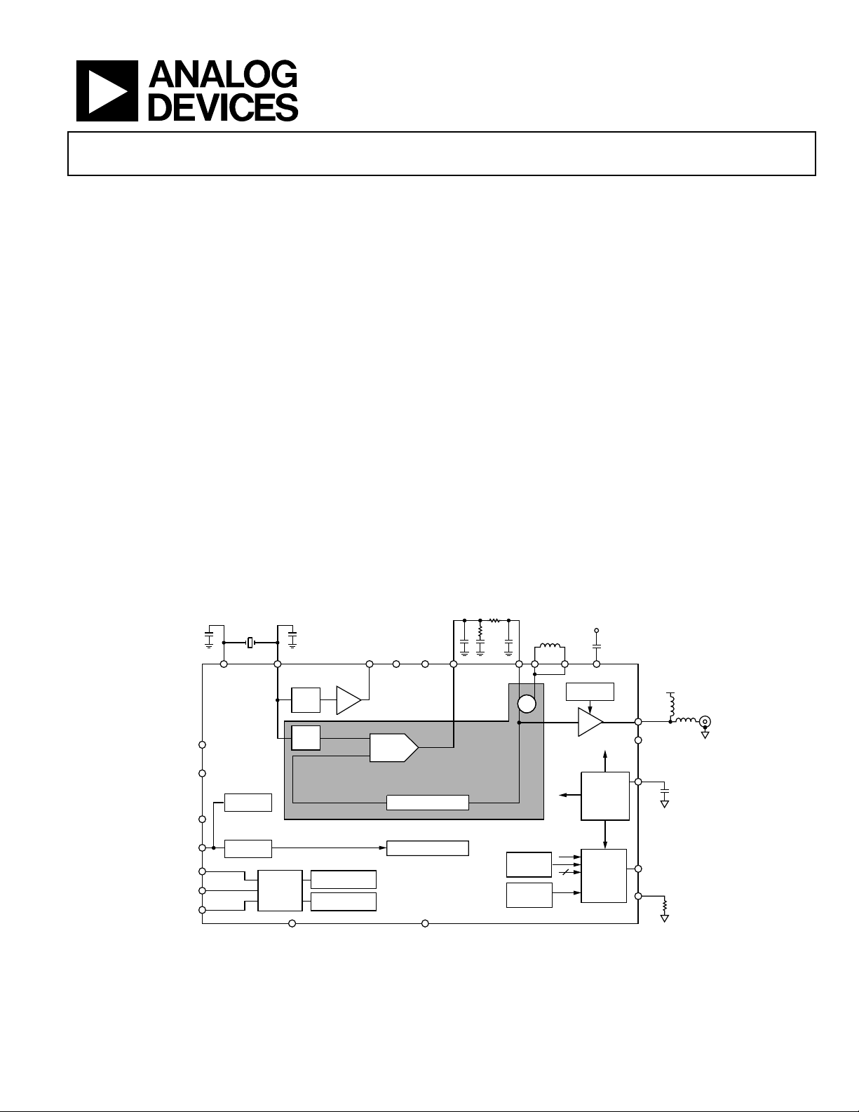
FSK/GFSK/OOK/GOOK/ASK Transmitter
ADF7012
GENERAL DESCRIPTION
The ADF7012 is a low power FSK/GFSK/OOK/GOOK/ASK
UHF transmitter designed for short range devices (SRDs). The
output power, output channels, deviation frequency, and modulation type are programmable by using four, 32-bit registers.
The fractional-N PLL and VCO with external inductor enable
the user to select any frequency in the 75 MHz to 1 GHz band.
The fast lock times of the fractional-N PLL make the ADF7012
suitable in fast frequency hopping systems. The fine frequency
deviations available and PLL phase noise performance facilitates
narrow-band operation.
There are five selectable modulation schemes: binary frequency
shift keying (FSK), Gaussian frequency shift keying (GFSK),
binary on-off keying (OOK), Gaussian on-off keying (GOOK),
and amplitude shift keying (ASK). In the compensation register,
the output can be moved in <1 ppm steps so that indirect compensation for frequency error in the crystal reference can be
made.
A simple 3-wire interface controls the registers. In power-down,
the part has a typical quiescent current of <0.1 μA.
FUNCTIONAL BLOCK DIAGRAM
CLK
CPVDDCP
CENTER
OUT
PFD/
CHARGE
PUMP
+FRACTIONAL N
OSC1 OSC2 L1 L2 C
÷CLK
SERIAL
INTERFACE
CE
÷R
FREQUENCY
COMPENSATION
FREQUENCY
DV
DD
D
GND
OOK\ASK
TxCLK
TxDATA
LE
DATA
CLK
Rev. 0
Information furnished by Analog Devices is believed to be accurate and reliable.
However, no responsibility is assumed by Analog Devices for its use, nor for any
infringements of patents or other rights of third parties that may result from its use.
Specifications subject to change without notice. No license is granted by implication
or otherwise under any patent or patent rights of Analog Devices. Trademarks and
registered trademarks are the property of their respective owners.
FSK\GFSK
GND
Σ-∆
A
GND
Figure 1.
C
PRINTED
INDUCTOR
VCO
PLL LOCK
DETECT
BATTERY
MONITOR
REG
OOK\ASK
PA
REGULATOR
MUXOUT
LDO
VCO
RF
OUT
RF GND
C
REG
MUXOUT
R
SET
V
DD
04617-0-001
One Technology Way, P.O. Box 9106, Norwood, MA 02062-9106, U.S.A.
Tel: 781.329.4700
Fax: 781.326.8703 © 2004 Analog Devices, Inc. All rights reserved.
www.analog.com

ADF7012
TABLE OF CONTENTS
Specifications..................................................................................... 3
GOOK Modulation.................................................................... 15
Timing Characteristics..................................................................... 5
Absolute Maximum Ratings............................................................ 6
Transis t o r Count ........................................................................... 6
ESD Caution.................................................................................. 6
Pin Configuration and Function Descriptions............................. 7
Typical Performance Characteristics ............................................. 8
315 MHz ........................................................................................ 8
433 MHz ........................................................................................ 9
868 MHz ......................................................................................10
915 MHz ......................................................................................11
Circuit Description......................................................................... 12
PLL Operation ............................................................................ 12
Crystal Oscillator........................................................................ 12
Crystal Compensation Register................................................ 12
Clock Out Circuit....................................................................... 12
Output Divider ........................................................................... 16
MUXOUT Modes....................................................................... 16
Theory of Operation ...................................................................... 17
Choosing the External Inductor Value.................................... 17
Choosing the Crystal/PFD Value............................................. 17
Tips on Designing the Loop Filter ........................................... 17
PA Mat c h ing................................................................................ 18
Transmit Protocol and Coding Considerations ..................... 18
Application Examples.................................................................... 19
315 MHz Operation................................................................... 20
433 MHz Operation................................................................... 21
868 MHz Operation................................................................... 22
915 MHz Operation................................................................... 23
Register Descriptions..................................................................... 24
R Register..................................................................................... 24
Loop Filter ................................................................................... 13
Volt a ge- C ont r o ll e d Os cil lato r (VCO ) ..................................... 13
Volt a ge R e gu l ator s ...................................................................... 13
FSK Modulation..........................................................................13
GFSK Modulation ...................................................................... 14
Power Amplifier.......................................................................... 14
REVISION HISTORY
10/04—Revision 0: Initial Version
N-Counter Latch ........................................................................ 25
Modulation Register .................................................................. 26
Function Register ....................................................................... 27
Outline Dimensions ....................................................................... 28
Ordering Guide .......................................................................... 28
Rev. 0 | Page 2 of 28
ADF7012
SPECIFICATIONS
DVDD = 2.3 V – 3.6 V; AGND = DGND = 0 V; TA = T
Table 1.
Parameter B Version Unit Conditions/Comments
RF OUTPUT CHARACTERISTICS
Operating Frequency 75/1000 MHz min/max
Phase Frequency Detector FRF/128 Hz min
MODULATION PARAMETERS
Data Rate FSK/GFSK 179.2 kbps Using 1 MHz loop bandwidth
Data Rate ASK/OOK 64 Kbps
Deviation FSK/GFSK PFD/2
511 × PFD/214Hz max For example, 10 MHz PFD – deviation max = ± 311.7 kHz
GFSK BT 0.5 typ
ASK Modulation Depth 25 dB max
OOK Feedthrough (PA Off) −40 dBm typ FRF = Fvco
−80 dBm typ FRF = Fvco/2
POWER AMPLIFIER PARAMETERS
Max Power Setting, DVDD = 3.6 V 14 dBm FRF = 915 MHz, PA is matched into 50 Ω
Max Power Setting, DVDD = 3.0 V 13.5 dBm FRF = 915 MHz, PA is matched into 50 Ω
Max Power Setting, DVDD = 2.3 V 12.5 dBm FRF = 915 MHz, PA is matched into 50 Ω
Max Power Setting, DVDD = 3.6 V 14.5 dBm FRF = 433 MHz, PA is matched into 50 Ω
Max Power Setting, DVDD = 3.0 V 14 dBm FRF = 433 MHz, PA is matched into 50 Ω
Max Power Setting, DVDD = 2.3 V 13 dBm FRF = 433 MHz, PA is matched into 50 Ω
PA Programmability 0.4 dB typ PA output = −20 dBm to +13 dBm
POWER SUPPLIES
DVDD 2.3/3.6 V min/V max
Current Comsumption
315 MHz, 0 dBm/5 dBm 8/14 mA typ DVDD = 3.0 V, PA is matched into 50 Ω, IVCO = min
433 MHz, 0 dBm/10 dBm 10/18 mA typ
868 MHz, 0 dBm/10 dBm/14 dBm 14/21/32 mA typ
915 MHz, 0 dBm/10 dBm/14 dBm
VCO Current Consumption 1/8 mA min/max VCO current consumption is programmable
Crystal Oscillator Current Consumption 190 µA typ
Regulator Current Consumption 280 µA typ
Power-Down Current 0.1/1 µA typ/max
REFERENCE INPUT
Crystal Reference Frequency 3.4/26 MHz min/max
Single-Ended Reference Frequency 3.4/26 MHz min/max
Crystal Power-On Time 3.4 MHz/26 MHz 1.8/2.2 ms typ CE to Clock Enable Valid
Single-Ended Input Level CMOS Levels
16/24/35 mA typ
to T
MIN
14
, unless otherwise noted. Operating temperature range is −40°C to +85°C.
MAX
VCO range adjustable using external inductor;
divide-by-2, -4, -8 options may be required
Based on US FCC 15.247 specfications for ACP; higher
data rates are achievable depending on local regulations
Hz min For example, 10 MHz PFD – deviation min = ± 610 Hz
Refer to the LOGIC INPUTS parameter. Applied to OSC 2 –
oscillator circuit disabled.
Rev. 0 | Page 3 of 28
ADF7012
Parameter B Version Unit Conditions/Comments
PHASE-LOCKED LOOP PARAMETERS
VCO Gain
315MHz 22 MHz/V typ VCO divide-by-2 active
433MHz 24 MHz/V typ VCO divide-by-2 active
868MHz 80 MHz/V typ
915MHz 88 MHz/V typ
VCO Tuning Range 0.3/2.0 V min/max
Spurious (IVCO Min/Max) −65/−70 dBc I
Charge Pump Current
Setting [00] 0.3 mA typ Refering to DB[7:6] in Function Register
Setting [01] 0.9 mA typ Refering to DB[7:6] in Function Register
Setting [10] 1.5 mA typ Refering to DB[7:6] in Function Register
Setting [11] 2.1 mA typ Refering to DB[7:6] in Function Register
Phase Noise (In band)
1
315MHz −85 dBc/Hz typ PFD = 10 MHz, 5 kHz offset, I
433MHz −83 dBc/Hz typ PFD = 10 MHz, 5 kHz offset, I
868MHz −80 dBc/Hz typ PFD = 10 MHz, 5 kHz offset, I
915MHz −80 dBc/Hz typ PFD = 10 MHz, 5 kHz offset, I
Phase Noise (Out of Band)1
315MHz −103 dBc/Hz typ PFD = 10 MHz, 1 MHz offset, I
433MHz −104 dBc/Hz typ PFD = 10 MHz, 1 MHz offset, I
868MHz −115 dBc/Hz typ PFD = 10 MHz, 1 MHz offset, I
915MHz −114 dBc/Hz typ PFD = 10 MHz, 1 MHz offset, I
Harmonic Content (Second)
2
−20 dBc typ FRF = F
Harmonic Content (Third)2 −30 dBc typ
Harmonic Content (Others)2 −27 dBc typ
Harmonic Content (Second)2 −24 dBc typ FRF = F
Harmonic Content (Third)2 −14 dBc typ
Harmonic Content (Others)2 −19 dBc typ
LOGIC INPUTS
Input High Voltage,V
Input Low Voltage, V
Input Current, I
INH/IINL
Input Capacitance, C
INH
INL
IN
0.7 × DV
0.2 × DV
DD
DD
V min
V max
±1 µA max
4.0 pF max
LOGIC OUTPUTS
Output High Voltage, V
OH
DVDD − 0.4 V min CMOS output chosen
Output High Current, IOH, 500 µA max
Output Low Voltage, V
OL
0.4 V max IOL = 500 µA
is programmable
VCO
VCO
/N (where N = 2, 4, 8)
VCO
= 2 mA
VCO
= 2 mA
VCO
= 3 mA
VCO
= 3 mA
VCO
VCO
VCO
VCO
VCO
= 2 mA
= 2 mA
= 3 mA
= 3 mA
1
Measurements made with N
2
Measurements made without harmonic filter.
FRAC
= 2048.
Rev. 0 | Page 4 of 28
ADF7012
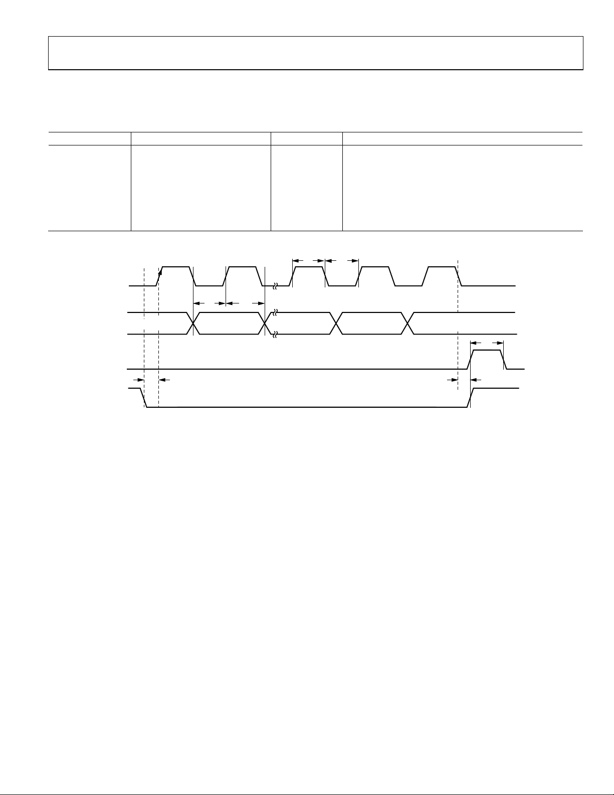
K
TIMING CHARACTERISTICS
DVDD = 3 V ± 10%; AGND = DGND = 0 V; TA = T
Table 2.
Parameter Limit at T
MIN
to T
(B Version) Unit Test Conditions/Comments
MAX
t1 20 ns min LE setup time
t2 10 ns min Data-to-clock setup time
t3 10 ns min Data-to-clock hold time
t4 25 ns min Clock high duration
t5 25 ns min Clock low duration
t6 10 ns min Clock –to-LE setup time
t7 20 ns min LE pulse width
MIN
to T
, unless otherwise noted.
MAX
CLOC
DATA
t
2
DB23 (MSB) DB22 DB2
LE
t
1
LE
t
t
4
3
t
5
DB1
(CONTROL BIT C2)
DB0 (LSB)
(CONTROL BIT C1)
t
6
t
7
04617-0-002
Figure 2. Timing Diagram
Rev. 0 | Page 5 of 28
ADF7012
ABSOLUTE MAXIMUM RATINGS
T
= 25°C, unless otherwise noted.
A
Table 3.
Parameter Rating
DVDD to GND
(GND = AGND = DGND = 0 V)
Digital I/O Voltage to GND −0.3 V to DVDD + 0.3 V
Analog I/O Voltage to GND −0.3 V to DVDD + 0.3 V
Operating Temperature Range
Maximum Junction Temperature 150°C
TSSOP θJA Thermal Impedance 150.4°C/W
Lead Temperature, Soldering
Vapor Phase (60 sec) 215°C
Infrared (15 sec) 220°C
−0.3 V to +3.9 V
ESD CAUTION
ESD (electrostatic discharge) sensitive device. Electrostatic charges as high as 4000 V readily accumulate on
the human body and test equipment and can discharge without detection. Although this product features
proprietary ESD protection circuitry, permanent damage may occur on devices subjected to high energy
electrostatic discharges. Therefore, proper ESD precautions are recommended to avoid performance
degradation or loss of functionality.
Stresses above those listed under Absolute Maximum Ratings
may cause permanent damage to the device. This is a stress
rating only; functional operation of the device at these or any
other conditions above those listed in the operational sections
of this specification is not implied. Exposure to absolute
maximum rating conditions for extended periods may affect
device reliability.
This device is a high performance RF integrated circuit with an
ESD rating of 1 kV and it is ESD sensitive. Proper precautions
should be taken for handling and assembly.
TRANSISTOR COUNT
35819 (CMOS)
Rev. 0 | Page 6 of 28
ADF7012
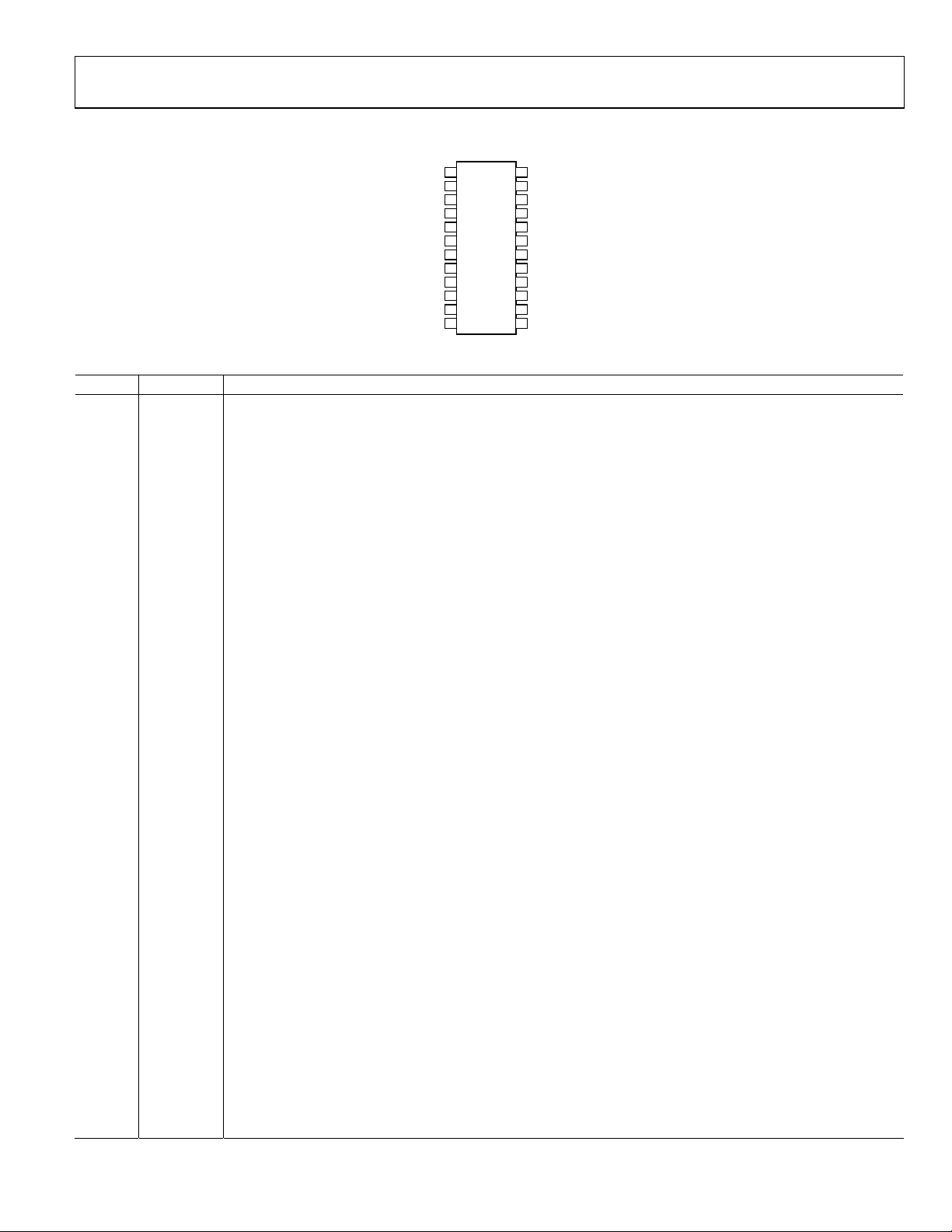
PIN CONFIGURATION AND FUNCTION DESCRIPTIONS
DV
1
DD
2
C
REG1
3
CP
OUT
4
TxDATA
TxCLK
5
DGND
OSC1
OSC2
OUT
CLK
DATA
ADF7012
6
TOP VIEW
(Not to Scale)
7
8
9
10
11
12
MUXOUT
CLK
Figure 3.
Table 4. Pin Functional Descriptions
Pin No. Mnemonic Description
1 DV
DD
Positive Supply for the Digital Circuitry. This must be between 2.3 V and 3.6 V. Decoupling capacitors to the analog
ground plane should be placed as close as possible to this pin.
2 C
REG1
A 2.2 µF capacitor should be added at C
REG
improves regulator power-on time, but may cause higher spurious noise.
3 CP
OUT
Charge Pump Output. This output generates current pulses that are integrated in the loop filter. The integrated
current changes the control voltage on the input to the VCO.
4 TxDATA Digital Data to Be Transmitted is inputted on this pin.
5 TxCLK
GFSK and GOOK only. This clock output is used to synchronize microcontroller data to the TxDATA pin of the
ADF7012. The clock is provided at the same frequency as the data rate. The microcontroller updates TxDATA on
the falling edge of TxCLK. The rising edge of TxCLK is used to sample TxDATA at the midpoint of each bit.
6 MUXOUT
Provides the Lock_Detect Signal. This determines if the PLL is locked to the correct frequency and also monitors
battery voltage. Other signals include Regulator_Ready, which indicates the status of the serial interface regulator.
7 DGND Ground for Digital Section.
8 OSC1 The reference crystal should be connected between this pin and OSC2.
9 OSC2
The reference crystal should be connected between this pin and OSC1. A TCXO reference may be used, by driving
this pin with CMOS levels, and powering down the crystal oscillator bit in software.
10 CLK
OUT
A divided-down version of the crystal reference with output driver. The digital clock output may be used to drive
several other CMOS inputs, such as a microcontroller clock. The output has a 50:50 mark-space ratio.
11 CLK
Serial Clock Input. This serial clock is used to clock in the serial data to the registers. The data is latched into the
32-bit shift register on the CLK rising edge. This input is a high impedance CMOS input.
12 DATA
Serial Data Input. The serial data is loaded MSB first with the two LSBs being the control bits. This is a high
impedance CMOS input.
13 LE
Load Enable, CMOS Input. When LE goes high, the data stored in the shift registers is loaded into one of the four
latches, the latch being selected using the control bits.
14 CE
Chip Enable. Bringing CE low puts the ADF7012 into complete power-down, drawing < 1uA. Register values are
lost when CE is low and the part must be reprogrammed once CE is brought high.
15 L1
Connected to external printed or discrete inductor. See Choosing the External Inductor Value for advice on the
value of the inductor to be connected between L1 and L2.
16 L2 Connected to external printed or discrete inductor.
17 C
VCO
A 220 nF capacitor should be tied between the C
This capacitor is necessary to ensure stable VCO operation.
18 VCO
19 RF
20 RF
IN
GND
OUT
The tuning voltage on this pin determines the output frequency of the voltage controlled oscillator (VCO). The
higher the tuning voltage, the higher the output frequency.
Ground for Output Stage of Transmitter.
The modulated signal is available at this pin. Output power levels are from –16 dBm to +12 dBm. The output
should be impedance matched using suitable components to the desired load. See the PA Matching section.
21 DV
DD
Voltage supply for VCO and PA section. This should have the same supply as DVDD Pin 1, and should be between
2.3 V and 3.6 V. Place decoupling capacitors to the analog ground plane as close as possible to this pin.
22 AGND Ground Pin for the RF Analog Circuitry.
23 R
24 C
SET
REG2
External Resistor to set charge pump current and some internal bias currents. Use 3.6 kV as default.
Add a 470 nF capacitor at C
to reduce regulator noise and improve stability. A reduced capacitor improves
REG
regulator power-on time and phase noise, but may have stability issues over the supply and temperature.
24
C
REG2
R
23
SET
AGND
22
TSSOP
21
DV
DD
RF
20
OUT
RF
19
GND
VCO
18
IN
C
17
VCO
16
L2
15
L1
CE
14
LE
13
04617-0-003
to reduce regulator noise and improve stability. A reduced capacitor
VCO
and C
pins. This line should run underneath the ADF7012.
REG2
Rev. 0 | Page 7 of 28
ADF7012
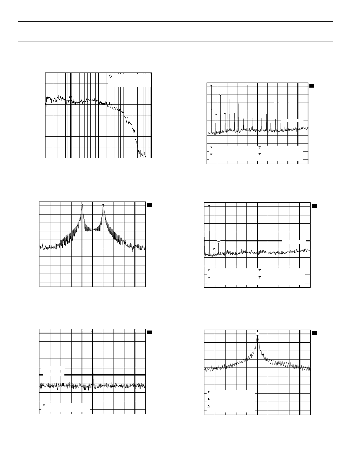
TYPICAL PERFORMANCE CHARACTERISTICS
315 MHZ
–60
–70
–80
–90
–100
dBc (Hz)
–110
–120
–130
–140
1.0k 10.0k 100.0k 1.0M 10.0M
PHASE NOISE (Hz)
Figure 4. Phase Noise Response—DV
IVCO = 2.0 mA, F
REF LVL
5dBm
5
0
–10
–20
–30
–40
–50
–60
–70
–80
–90
–95
CENTER 315MHz 50kHz/ SPAN 500kHz
= 315 MHz, PFD = 3.6864 MHZ, PA Bias = 5.5 mA
OUT
0.45dBm
315.05060120MHz
Figure 5. FSK Modulation, Power = 0 dBm, Data Rate = 1 kbps,
F
= ±50 kHz
DEVIATION
REF LVL
5dBm
5
0
–10
–20
–30
–40
D1 –41.5dBm
D2 –49dBm
–50
–60
–70
–80
1 [T1] 0.31dBm
–90
–95
CENTER 315MHz 40MHz/
0.31dBm
315.40080160MHz
315.40080160MHz
Figure 6. Spurious Components—Meets FCC Specs
= NORMAL
FREQUENCY = 9.08 kHz
LEVEL = –84.47dBc/Hz
= 3.0 V, ICP = 0.86 mA
DD
RBW
5kHz
VBW
5kHz
SWT
500ms
21
RBW
500kHz
VBW
500kHz
SWT
5ms
1
30dB
RF ATT
dBm
UNIT
30dB
RF ATT
dBm
UNIT
SPAN 400MHz
04617-0-004
A
1MA
04617-0-005
A
1MA
04617-0-006
REF LVL
5dBm
5
1
0
–10
–20
–30
–40
–50
–60
–70
–80
–90
–95
3
4
2
1 [T1] 0.27dBm
2 [T1]
0.27dBm
308.61723447MHz
308.61723447MHz
–35.43dBm
631.26252505MHz
Figure 7. Harmonic Response, RF
REF LVL
5dBm
5
1
0
–10
–20
–30
–40
–50
–60
–70
–80
–90
–95
3
2
4
1 [T1] 0.18dBm
308.61723447MHz
2 [T1]
631.26252505MHz
CENTER 3.5MHz 700MHz/
0.18dBm
308.61723447MHz
–50.53dBm
RBW
1MHz
VBW
1MHz
SWT
17.5ms
3 [T1]
939.87975952MHz
4 [T1]
1.26252505GHz
Matched to 50 Ω, No Filter
OUT
RBW
1MHz
VBW
1MHz
SWT
17.5ms
3 [T1]
939.87975952MHz
4 [T1]
1.26252505GHz
RF ATT
UNIT
D1 –41.5dBm
–11.48dBm
–34.11dBm
RF ATT
UNIT
D1 –41.5dBm
–42.93dBm
–55.48dBm
SPAN 7GHz
30dB
dBm
1MA
30dB
dBm
Figure 8. Harmonic Response, Fifth-Order Butterworth Filter
REF LVL
5dBm
5
0
–10
–20
–30
–40
–50
–60
1 [T1] –3.49dBm
–70
3 [T1]
–80
2 [T1]
–90
–95
20.33dBm
26.55310621kHz
2 3
315.00012525MHz
–20.33dB
26.55310621kHz
–20.85dB
–27.55511022kHz
RBW
VBW
SWT
1
5kHz
5kHz
500ms
RF ATT
UNIT
dBm
30dB
Figure 9. OOK Modulation, Power = 0 dBm, Data Rate = 10 kbps
A
04617-0-007
A
SGL
1MA
04617-0-008
A
1MA
04617-0-009
Rev. 0 | Page 8 of 28
ADF7012
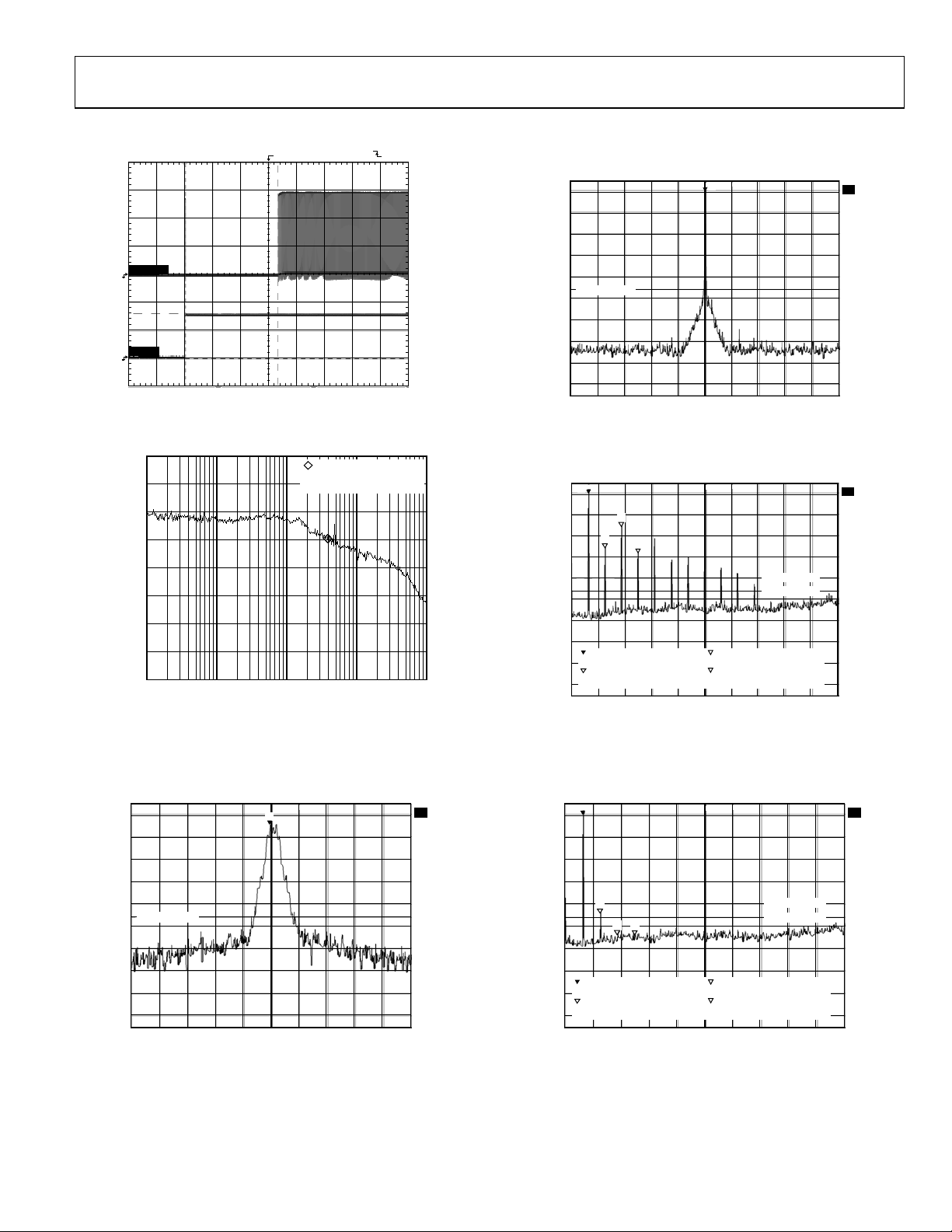
433 MHZ
40dB
2 1.00V/ 1.50ms 720mv500µs TRIG'D 1
1 2.00V/
2
CLKOUT
1
CE
Figure 10. Crystal Power-On Time, 4 MHz, Time = 1.6 ms
–40
–60
–80
–100
–120
dBc (Hz)
–140
–160
–180
–200
1.0k 10.0k 100.0k 1.0M 10.0M
PHASE NOISE (Hz)
Figure 11. Phase Noise Response—ICP = 2.0 mA, I
RF
= 433.92 MHz, PFD = 4 MHz, PA Bias = 5.5 mA
OUT
REF LVL
15dBm
15
10
0
–10
–20
–30
D1 –36dBm
–40
–50
–60
–70
–80
–85
START 433.05MHz 174kHz/ STOP 434.79kHz
5.60dBm
433.91158317MHz
= NORMAL
FREQUENCY = 393.38 kHz
LEVEL = –102.34dBc/Hz
RBW
10kHz
VBW
300kHz
SWT
44ms
1
VCO
RF ATT
UNIT
= 2.0 mA,
40dB
dBm
04617-0-010
A
1MA
04617-0-012
04617-0-011
REF LVL
15dBm
15
10
0
–10
–20
–30
D1 –36dBm
–40
–50
–60
–70
–80
–85
CENTER 433.9500601MHz 3.2MHz/ SPAN 32MHz
10.01dBm
433.91158317MHz
RBW
VBW
SWT
1
Figure 13. Spurious Components—Meets ETSI Specs
REF LVL
15dBm
15
1
10
0
–10
–20
–30
–40
–50
–60
–70
–80
–85
2
1 [T1] 10.10dBm
2 [T1]
CENTER 3.5GHz 700MHz/ SPAN 7GHz
10.10dBm
434.86973948MHz
3
4
434.86973948MHz
–15.25dBm
869.73947896MHz
Figure 14. Harmonic Response, RF
REF LVL
15dBm
15
1
10
0
–10
–20
–30
–40
–50
–60
–70
–80
–85
2
3
1 [T1] 9.51dBm
434.86973948MHz
2 [T1]
869.73947896MHz
CENTER 3.5GHz 700MHz/ SPAN 7GHz
9.51dBm
434.86973948MHz
4
–33.75dBm
RBW
VBW
SWT
3 [T1]
4 [T1]
Matched to 50 Ω, No Filter
OUT
RBW
VBW
SWT
3 [T1]
4 [T1]
30kHz
30kHz
90ms
1MHz
1MHz
17.5ms
D1 –30dBm
D1 –36dBm
1.30460922GHz
–17.57dBm
1.73947896GHz
1MHz
1MHz
17.5ms
D1 –30dBm
D1 –36dBm
–43.60dBm
1.30460922GHz
–43.44dBm
1.73947896GHz
RF ATT
UNIT
RF ATT
UNIT
–5.12dBm
RF ATT
UNIT
dBm
A
1MA
04617-0-013
40dB
dBm
A
1MA
04617-0-014
40dB
dBm
A
SGL
1MA
04617-0-015
Figure 12. FSK Modulation, Power = 10 dBm, Data Rate = 38.4 kbps, F
= ±19.28 kHz
DEVIATION
Rev. 0 | Page 9 of 28
Figure 15. Harmonic Response, Fifth-Order Butterworth Filter

ADF7012
868 MHZ
0
–20
–40
–60
–80
dBc (Hz)
–100
–120
–140
–160
1.0k 10.0k 100.0k 1.0M 10.0M
Figure 16. Phase Noise Response–I
PHASE NOISE (Hz)
= 2.5 mA, I
CP
MHz, PFD = 4.9152 MHz, Power = 12.5 dBm, PA Bias = Max
REF LVL
15dBm
15
10
0
–10
1MAX
–20
–30
–40
–50
–60
1 [T1] 40.44dBm
–70
2 [T1]
–80
–85
CENTER 868.944489MHz 60kHz/ SPAN 600kHz
–40.44dBm
869.20000000MHz
D2 –36dBm
869.20000000MHz
8.02dBm
868.96673347MHz
Figure 17. FSK Modulation, Power = 12.5 dBm, Data Rate = 38.4 kbps,
F
= ±19.2 kHz
DEVIATION
REF LVL
15dBm
15
10
0
–10
1MAX
–20
–30
–40
–50
–60
–70
–80
–85
2
START 856.5MHz 2.5MHz/ STOP 881.5MHz
12.55dBm
869.025050100MHz
3
1
Figure 18. Spurious Components—Meets ETSI Specs
= NORMAL
FREQUENCY = 251.3 kHz
LEVEL = –99.39dBc/Hz
= 1.44 mA, RF
VCO
RBW
VBW
SWT
2
RBW
VBW
SWT
1 [T1] 12.55dBm
2 [T1]
3 [T1]
RF ATT
10kHz
MIXER
10kHz
UNIT
15ms
RF ATT
2kHz
MIXER
2kHz
UNIT
16s
869.02505010MHz
–57.89dBm
859.16695500MHz
–81.97dBm
862.00000000MHz
D2 –36dBm
D1 –54dBm
–20dBm
–20dBm
30dB
dBm
1
30dB
dBm
= 868.95
OUT
A
LN
1MA
04617-0-017
A
LN
1MA
04617-0-018
04617-0-016
RBW
REF LVL
15dBm
15
1
10
0
–10
1MAX
–20
–30
–40
–50
–60
1 [T1] 12.27dBm
–70
2 [T1]
–80
–85
CENTER 3.8GHz 640MHz/ SPAN 6.4GHz
12.27dBm
869.33867735MHz
2
3
869.33867735MHz
–4.00dBm
1.72865731GHz
4
Figure 19. Harmonic Response, RF
REF LVL
15dBm
15
1
10
0
–10
1MAX
–20
–30
D2 –30dBm
–40
–50
–60
–70
–80
–85
START 3.8GHz 640MHz/ SPAN 6.4GHz
2
10.39dBm
869.33867735MHz
3
1MHz
VBW
1MHz
SWT
16ms
3 [T1]
4 [T1]
Matched to 50 Ω, No Filter
OUT
RBW
1kHz
VBW
1kHz
SWT
10ms
1 [T1] 10.39dBm
3 [T1]
2 [T1]
Figure 20. Harmonic Response, Fifth-Order Chebyshev Filter
40dB
RF ATT
dBm
UNIT
D1 –30dBm
–16.88dBm
2.59699399GHz
–15.06dBm
3.46913828GHz
RF ATT
MIXER
UNIT
869.33867735MHz
1.72000000GHz
2.59600000GHz
30dB
–20dBm
–50.92dBm
–50.40dBm
A
1MA
04617-0-019
dBm
A
LN
1MA
04617-0-020
Rev. 0 | Page 10 of 28

ADF7012
915 MHZ
40dB
–40
–60
–80
–100
–120
dBc (Hz)
–140
–160
–180
–200
1.0k 10.0k 100.0k 1.0M 10.0M
Figure 21. Phase Noise Response–I
PHASE NOISE (Hz)
CP
= NORMAL
FREQUENCY = 992.38 kHz
LEVEL = –102.34dBc/Hz
= 1.44 mA, I
VCO
= 3.0 mA, RF
MHz, PFD =10 MHz, Power = 10 dBm, PA Bias = 5.5 mA
10kHz
300kHz
15ms
RF ATT
UNIT
dBm
REF LVL
15dBm
15
10
0
–10
1MAX
–20
–30
–40
–50
–60
–70
–80
–85
CENTER 915.190982MHz 50kHz/ SPAN 500kHz
3.88dBm
915.19098196MHz
RBW
VBW
SWT
1
40dB
Figure 22. FSK Modulation, Power = 10 dBm, Data Rate = 38.4 kbps,
Fdeviation = ±19.2 kHz
10kHz
300kHz
100ms
RF ATT
UNIT
dBm
REF LVL
15dBm
15
10
0
–10
–20
–30
–40
D1 –41.5dBm
D1 –49.5dBm
–50
–60
–70
–80
–85
CENTER 915.2MHz 40MHz/ SPAN 400MHz
9.94dBm
915.23167977MHz
RBW
VBW
SWT
1
40dB
Figure 23. Spurious Components—Meets FCC Specs
= 915.2
OUT
1MA
SGL
1MA
04617-0-021
A
04617-0-036
*
A
04617-0-037
REF LVL
15dBm
15
1
10
0
–10
1MAX
–20
–30
–40
–50
–60
1 [T1] 10.25dBm
–70
2 [T1]
–80
–85
CENTER 3.8GHz 640MHz/ SPAN 6.4GHz
10.25dBm
907.81563126MHz
2
3
907.81563126MHz
–10.06dBm
1.83126253GHz
Figure 24. Harmonic Response, RF
REF LVL
15dBm
15
1
10
0
–10
1MAX
–20
–30
–40
–50
–60
–70
–80
–85
CENTER 3.8GHz 640MHz/ SPAN 6.4GHz
2
1 [T1] 9.06dBm
907.81563126MHz
2 [T1]
9.06dBm
907.81563126MHz
3
–48.40dBm
1.83126253GHz
RBW
VBW
SWT
4
3 [T1]
4 [T1]
Matched to 50 Ω, No Filter
OUT
RBW
VBW
SWT
D1 –41.5dBm
4
3 [T1]
4 [T1]
Figure 25. Harmonic Response, Fifth-Order Chebyshev Filter
RF ATT
50MHz
50MHz
UNIT
6.4s
D1 –41.5dBm
–20.29dBm
2.74188377GHz
–17.50dBm
3.65250501GHz
RF ATT
50MHz
50MHz
UNIT
6.4s
–46.22dBm
2.74188377GHz
–46.96dBm
3.65250501GHz
dBm
A
1MA
04617-0-038
40dB
dBm
A
1MA
04617-0-039
Rev. 0 | Page 11 of 28

ADF7012
CIRCUIT DESCRIPTION
PLL OPERATION
A fractional-N PLL allows multiple output frequencies to be
generated from a single-reference oscillator (usually a crystal)
simply by changing the programmable N value found in the N
register. At the phase frequency detector (PFD), the reference is
compared to a divided-down version of the output frequency
(VCO/N). If VCO/N is too low a frequency, typically the output
frequency is lower than desired, and the PFD and charge-pump
combination sends additional current pulses to the loop filter.
This increases the voltage applied to the input of the VCO.
Because the VCO of the ADF7012 has a positive frequency vs.
voltage characteristic, any increase in the Vtune voltage applied
to the VCO input increases the output frequency at a rate of kV,
the tuning sensitivity of the VCO (MHz/V). At each interval of
1/PFD seconds, a comparison is made at the PFD until the PFD
and charge pump eventually force a state of equilibrium in the
PLL where PFD frequency = VCO/N. At this point, the PLL can
be described as locked.
CRYSTAL/R
LOOP FILTER
N
Figure 26.
VCO
FVCO
04617-0-022
VCO/N
R
PFD
CP
OSC1
OSC2
CP1CP2
Figure 27.
04617-0-023
Two parallel resonant capacitors are required for oscillation at
the correct frequency—the value of these depend on the crystal
specification. They should be chosen so that the series value of
capacitance added to the PCB track capacitance adds to give the
load capacitance of the crystal, usually 20 pF. Track capacitance
values vary between 2 pF to 5 pF, depending on board layout.
Where possible, to ensure stable frequency operation over all
conditions, capacitors should be chosen so that they have a very
low temperature coefficient and/or opposite temperature
coefficients
CRYSTAL COMPENSATION REGISTER
The ADF7012 features a 15-bit fixed modulus, which allows the
output frequency to be adjusted in steps of FPFD/15. This fine
resolution can be used to easily compensate for initial error and
temperature drift in the reference crystal.
= F
F
ADJUST
× FEC (3)
STEP
OUT
=
CRYSTAL
R
F
PFD
NF
×=
(1)
NF
×
For a Fractional N PLL
N
⎞
FRAC
(2)
⎟
12
2
⎠
where N
⎛
+×=
NFF
⎜
INTPFDOUT
⎝
can be bits M1 to M12 in the fractional N register.
FRAC
CRYSTAL OSCILLATOR
The on-board crystal oscillator circuitry (Figure 27) allows an
inexpensive quartz crystal to be used as the PLL reference. The
oscillator circuit is enabled by setting XOEB low. It is enabled by
default on power-up and is disabled by bringing CE low. Errors
in the crystal can be corrected using the error correction
register within the R register.
A single-ended reference may be used instead of a crystal, by
applying a square wave to the OSC2 pin, with XOEB set high.
where F
= FPFD/215 and FEC = Bits F1 to F11 in the R
STEP
Register. Note that the notation is twos compliment, so F11
represents the sign of the FEC number.
Example
= 10 MHz
F
PFD
= −11 kHz
F
ADJUST
F
= 10 MHz/215 = 305.176 Hz
STEP
FEC = −11 kHz/305.17 Hz = −36 = −(00000100100) =
11111011100 = 0x7DC
CLOCK OUT CIRCUIT
The clock out circuit takes the reference clock signal from the
oscillator section above and supplies a divided-down 50:50
mark-space signal to the CLK
2 to 30 is available. This divide is set by the DB[19:22] in the R
register. On power-up, the CLK
OSC1
DIVIDER
1 TO 15
pin. An even divide from
OUT
defaults to divide by 16.
OUT
DV
DD
CLK
ENABLE BIT
÷2
Figure 28.
CLK
OUT
OUT
04617-0-024
Rev. 0 | Page 12 of 28

ADF7012
The output buffer to CLK
the function register high. On power-up, this bit is set high.
The output buffer can drive up to a 20 pF load with a 10% rise
time at 4.8 MHz. Faster edges can result in some spurious
feedthrough to the output. A small series resistor (50 Ω) can be
used to slow the clock edges to reduce these spurs at F
LOOP FILTER
The loop filter integrates the current pulses from the charge
pump to form a voltage that tunes the output of the VCO to the
desired frequency. It also attenuates spurious levels generated by
the PLL. A typical loop filter design is shown in Figure 29.
CHARGE
PUMP OUT
In FSK, the loop should be designed so that the loop bandwidth
(LBW) is a minimum of two to three times the data rate.
Widening the LBW excessively reduces the time spent jumping
between frequencies, but results in reduced spurious
attenuation. See the section Tips on Designing the Loop Filter.
For OOK/ASK systems, a wider loop bandwidth than for FSK
systems is desirable. The sudden large transition between two
power levels results in VCO pulling (VCO temporarily goes to
incorrect frequency) and can cause a wider output spectrum.
By widening the loop bandwidth a minimum of 10 × data rate,
VCO pulling is minimized because the loop settles quickly back
to the correct frequency. The free design tool ADIsimPLL™ can
be used to design loop filters for the ADI family of transmitters.
VOLTAGE-CONTROLLED OSCILLATOR (VCO)
The ADF7012 features an on-chip VCO with an external tank
inductor, which is used to set the frequency range. The center
frequency of oscillation is governed by the internal varactor
capacitance and that of the external inductor combined with the
bond-wire inductance. An approximation for this is given in the
Equation 4. For a more accurate selection of the inductor, see
the section Choosing the External Inductor Value.
F
VCO
The varactor capacitance can be adjusted in software to increase
the effective VCO range by writing to bits VA1 and VA2 in the
R register. Under typical conditions, setting VA1 and VA2 high
increases the center frequency by reducing the varactor
capacitance by approximately 1.3 pF.
is enabled by setting Bit DB4 in
OUT
VCO
Figure 29.
1
()
CCLL
+×+=)(π2
(4)
FIXEDVAREXTINT
.
CLK
04617-0-025
Figure 32 shows the VCO gain over temperature and frequency.
VCO gain is important in determining the loop filter design—
predictable changes in VCO gain resulting in a change in the
loop filter bandwidth can be offset by changing the chargepump current in software.
VCO Bias Current
VCO bias current may be adjusted using bits VB1 to VB4 in the
function register. Additional bias current will reduce spurious
levels, but increase overall current consumption in the part. A
bias value of 0x5 should ensure oscillation at most frequencies
and supplies. Settings 0x0, 0xE ,and 0xF are not recommended.
Setting 0x3 and Setting 0x4 are recommended under most
conditions. Improved phase noise can be achieved for lower
bias currents.
VOLTAGE REGULATORS
There are two band gap voltage regulators on the ADF7012
providing a stable 2.25 V internal supply: a 2.2 µF capacitor
(X5R, NP0) to ground at C
and a 470 nF capacitor at C
REG1
REG2
should be used to ensure stability. The internal reference
ensures consistent performance over all supplies and reduces
the current consumption of each of the blocks.
The combination of regulators, band gap reference, and biasing
typically consume 1.045 mA at 3.0 V and can be powered down
by bringing the CE line low. The serial interface is supplied by
Regulator 1, so powering down the CE line causes the contents
of the registers to be lost. The CE line must be high and the
regulators must be fully powered on to write to the serial
interface. Regulator power-on time is typically 100 µs and
should be taken into account when writing to the ADF7012
after power-up. Alternatively, regulator status may be monitored
at the MUXOUT pin once CE has been asserted, because
MUXOUT defaults to the regulator ready signal. Once
Regulator_ready is high, the regulator is powered up and the
serial interface is active.
FSK MODULATION
FSK modulation is performed internally in the PLL loop by
switching the value of the N register based on the status of the
TxDATA line. The TxDATA line is sampled at each cycle of the
PFD block (every 1/F
to-high transition, an N value representing the deviation
frequency is added to the N value representing the center
frequency. Immediately the loop begins to lock to the new
frequency of F
CENTER
makes a high-to-low transition, the N value representing the
deviation is subtracted from the PLL N value representing the
center frequency and the loop transitions to F
seconds). When TxDATA makes a low-
PFD
+ F
. Conversely, when TxDATA
DEVIATION
CENTER
− F
DEVIATION
.
Rev. 0 | Page 13 of 28

ADF7012
PFD/
CHARGE
PUMP
THIRD-ORDER
Σ-∆ MODULATOR
Figure 30.
INTEGER-NFRACTIONAL-N
FSK DEVIATION
FREQUENCY
–F
DEV
+F
DEV
TxDATA
4R
The deviation from the center frequency is set using bits D1 to
D9 in the modulation register. The frequency deviation may be
set in steps of
STEP
HzF =
(5)
14
2
F
PFD
)(
The deviation frequency is therefore
DEVIATION
×
PFD
)(
HzF
=
NumberModulationF
14
2
where ModulationNumber is set by bits D1 to D9.
The maximum data rate is a function of the PLL lock time (and
the requirement on FSK spectrum). Because the PLL lock time
is reduced by increasing the loop-filter bandwidth, highest data
rates can be achieved for the wider loop filter bandwidths. The
absolute maximum limit on loop filter bandwidth to ensure
stability for a fractional-N PLL is F
/7. For a 20 MHz PFD
PFD
frequency, the loop bandwidth could be as high as 2.85 MHz.
FSK modulation is selected by setting bits S1 and S2 in the
modulation register low.
VCO
÷N
(6)
PA STAGE
04617-0-026
For GFSK and GOOK, the incoming bit stream to be transmitted needs to be synchronized with an on-chip sampling
clock which provides one sample per bit to the Gaussian FIR
filter. To facilitate this, the sampling clock is routed to the
TxCLK pin where data is fetched from the host microcontroller
or microprocessor on the falling edge of TxCLK, and the data is
sampled at the midpoint of each bit on TxCLK’s rising edge.
Inserting external RC LPFs on TxDATA and TxCLK lines
creates smoother edge transitions and improves spurious
performance. As an example, suitable components would be a
1 kV resistor and 10 nF capacitor for a data rate of 5 kbps.
I/O
µC
INT
FETCH
FETCH
SAMPLE
Fig ure 31. TxC LK/ TxDATA S ync hron iza tion.
SAMPLE
FETCH
FETCH
SAMPLE
TxDATA
ADF7012
TxCLK
The number of steps between symbol ‘0’ and symbol ‘1’ is
determined by the setting for the index counter.
The GFSK deviation is set up as
GFSK
DEVIATION
)Hz(×=
F
PFD
m
2
(7)
12
2
where m is the mod control (Bits MC1 to MC3 in the
modulation register).
The GFSK sampling clock samples data at the data rate:
F
bpsDataRate
=)(
PFD
×
erIndexCounttorDividerFac
(8)
where DividerFactor can be bits D1 to D7, and IndexCounter
can be bits IC1 and IC2 in the modulation register.
04617-0-040
GFSK MODULATION
Gaussian Frequency Shift Keying, or GFSK, represents a filtered
form of frequency shift keying. The data to be modulated to RF
is prefiltered digitally using an finite impulse response filter
(FIR). The filtered data is then used to modulate the sigmadelta fractional-N to generate spectrally-efficient FSK.
FSK consists of a series of sharp transitions in frequency as the
data is switched from one level to an other. The sharp switching
generates higher frequency components at the output, resulting
in a wider output spectrum.
With GFSK, the sharp transitions are replaced with up to 128
smaller steps. The result is a gradual change in frequency. As a
result, the higher frequency components are reduced and the
spectrum occupied is reduced significantly. GFSK does require
some additional design work as the data is only sampled once
per bit, and so the choice of crystal is important to ensure the
correct sampling clock is generated.
Rev. 0 | Page 14 of 28
POWER AMPLIFIER
The output stage is based on a Class E amplifier design, with an
open drain output switched by the VCO signal. The output
control consists of six current mirrors operating as a
programmable current source.
To achieve maximum voltage swing, the RF
biased at DV
. A single pull-up inductor to DVDD ensures a
DD
current supply to the output stage, PA biased to DV
with the correct choice of value transforms the impedance.
The output power can be adjusted by changing the value of
bits P1 to P6. Typically, this is P1 to P6 output −20dBm at 0x0,
and 13 dBm at 0x7E at 868MHz, with the optimum matching
network.
pin needs to be
OUT
volts, and
DD

ADF7012
The nonlinear characteristic of the output stage results in an
output spectrum containing harmonics of the fundamental,
especially the third and fifth. To meet local regulations, a lowpass filter usually is required to filter these harmonics.
The output stage can be powered down by setting Bit PD2 in
the function register low.
GOOK MODULATION
Gaussian on-off keying (GOOK) represents a prefiltered form
of OOK modulation. The usually sharp symbol transitions are
replaced with smooth Gaussian-filtered transitions with the
result being a reduction in frequency pulling of the VCO.
Frequency pulling of the VCO in OOK mode can lead to a
wider than desired bandwidth, especially if it is not possible to
increase the loop filter bandwidth to > 300kHz.
The GOOK sampling clock samples data at the data rate:
F
bpsDataRate
=)(
PFD
×
Bits D1 to D6 represent the output power for the system for a
positive data bit. Divider Factor = 0x3F represents the max-
imum possible deviation from PA at minimum to PA at
maximum output. An index counter setting of 128 is
recommended.
Figure 32 shows the step response of the Gaussian FIR filter.
An index counter of 16 is demonstrated for simplicity. While
the pre-filter data would switch the PA directly from off to on
with a low-to-high data transition, the filtered data gradually
increases the PA output in discrete steps. This has the effect of
making the output spectrum more compact.
PRE-FILTER DATA
(0 TO 1 TRANSITION)
PA SETTING
16 (MAX)
15
14
13
12
11
10
9
8
7
6
5
4
3
2
1 (PA OFF)
Figure 32. Varying PA Output for GOOK (Index Counter = 16).
DISCRETIZED
FILTER OUTPUT
(9)
erIndexCounttorDividerFac
04617-0-041
As is the case with GFSK, GOOK requires the bit stream
applied at TxDATA to be synchronized with the sampling clock,
TxCLK (see the GFSK Modulation section).
10
0
–10
–20
–30
–40
POWER (dBm)
–50
–60
–70
–80
909.43 910.43
20
10
0
–10
–20
–30
–40
POWER (dBm)
–50
–60
–70
–80
–90
885.43 910.43 935.93
OOK
GOOK
FREQUENCY (MHz)
Figure 33. GOOK vs. OOK Frequency Spectra
(Narrow-Band Measurement)
OOK
GOOK
FREQUENCY (MHz)
Figure 34. GOOK vs. OOK Frequency Spectra
(Wideband Measurement)
910.93
04617-0-043
04617-0-044
Rev. 0 | Page 15 of 28

ADF7012
OUTPUT DIVIDER
An output divider is a programmable divider following the
VCO in the PLL loop. It is useful when using the ADF7012 to
generate frequencies of < 500 MHz.
REFERENCE
DIVIDER
PFD CP PA
Figure 35. Output Divider Location in PLL.
LOOP
FILTER
÷N
VCO
OUTPUT
DIVIDER
÷1/2/4/8
04617-0-042
The output divider may be used to reduce feedthrough of the
VCO by amplifying only the VCO/2 component, restricting the
VCO feedthrough to leakage.
Because the divider is in loop, the N register values should be
set up according to the usual formula. However, the VCO gain
) should be scaled according to the divider setting, as shown
(K
V
in the following example.
Fout = 433 MHz, Fvco = 866 MHz, K
@ 868 MHz =
V
60 MHz/V
Therefore, K
for loop filter design = 30 MHz/V.
V
The divider value is set in the R register.
Table 5.
OD1 OD2 Divider Status
0 0 Divider off
0 1 Divide by 2
1 0 Divide by 4
1 1 Divide by 8
MUXOUT MODES
The MUXOUT pin allows the user access to various internal
signals in the transmitter, and provides information on the
PLL lock status, the regulator, and the battery voltage. The
MUXOUT is accessed by programming Bits M1 to M4 in the
function register and observing the signal at the MUXOUT pin.
Battery Voltage Read back
By setting MUXOUT to 1010 to 1101, the battery voltage can be
estimated. The battery measuring circuit features a voltage
divider and a comparator where the divided-down supply
voltage is compared to the regulator voltage.
Table 6.
MUXOUT MUXOUT High MUXOUT Low
1010 DVDD > 3.25 V DVDD < 3.25 V
1011 DVDD > 3.0 V DVDD < 3.0 V
1100 DVDD > 2.75 V DVDD < 2.75 V
1101 DVDD > 2.35 V DVDD < 2.35 V
The accuracy of the measurement is limited by the accuracy of
the regulator voltage and also the internal resistor tolerances.
Regulator Ready
The regulator has a power-up time, dependant on process and
the external capacitor. The regulator ready signal indicates that
the regulator is fully powered, and that the serial interface is
active. This is the default setting on power-up at MUXOUT.
Digital Lock Detect
Digital lock detect indicates that the status of the PLL loop.
The PLL loop takes time to settle on power-up and when the
frequency of the loop is changed by changing the N value.
When lock detect is high, the PFD has counted a number of
consecutive cycles where the phase error is < 15 ns. The lock
detect precision bit in the function register determines whether
this is 3 cycles (LDP = 0), or 5 cycles (LDP=1). It is recommended that LDP be set to 1. The lock detect is not completely
accurate and goes high before the output has settled to exactly
the correct frequency. In general, add 50% to the indicated
lock time to obtain lock time to within 1 kHz. The lock detect
signal can be used to decide when the power amplifier (PA)
should be enabled.
R Divider
MUXOUT provides the output of the R divider. This is a
narrow pulsed digital signal at frequency F
be used to check the operation of the crystal circuit and the R
divider. R divider/2 is a buffered version of this signal at F
. This signal may
PFD
PFD
/2.
Rev. 0 | Page 16 of 28

ADF7012
THEORY OF OPERATION
CHOOSING THE EXTERNAL INDUCTOR VALUE
The ADF7012 allows operation at many different frequencies by
choosing the external VCO inductor to give the correct output
frequency. Figure 36 shows both the minimum and maximum
frequency vs. the inductor value. These are measurements based
on 0603 CS type inductors from Coilcraft, and are intended as
guidelines in choosing the inductor because board layout and
inductor type varies between applications.
The inductor value should be chosen so it is between the
minimum and maximum value.
1200
1100
1000
900
800
700
600
FREQUENCY (MHz)
500
400
300
010515203025 35
Figure 36. Output Frequency vs. External Inductor Value
INDUCTANCE (nH)
Ibias = 2.0 mA.
MIN (meas)
MAX (meas)
MIN (eqn)
MAX (eqn)
04617-0-031
For frequencies between 270 MHz and 550 MHz, it is
recommended to operate the VCO at twice the desired output
frequency and use the divide-by-2 option. This ensures reliable
operation over temperature and supply.
For frequencies between 130 MHz and 270 MHz, it is
recommended to operate the VCO at four times the desired
output frequency and use the divide-by-4 option.
For frequencies below 130 MHz, it is best to use the divide-by-8
option. It is not necessary to use the VCO divider for
frequencies above 550 MHz.
ADIsimPLL is a PLL design tool which can perform the
frequency calculations for the ADF7012, and is available at
www.analog.com/pll.
CHOOSING THE CRYSTAL/PFD VALUE
The choice of crystal value is an important one. The PFD
frequency must be the same as the crystal value or an integer
division of it. The PFD determines the phase noise, spurious
levels and location, deviation frequency, and the data rate in the
case of GFSK. The following sections describe some factors that
should be considered when choosing the crystal value.
Standard Crystal Values
Standard crystal values are 3.6864 MHz, 4 MHz, 4.096 MHz,
4.9152 MHz, 7.3728 MHz, 9.8304 MHz, 10 MHz, 11.0592 MHz,
12 MHz, and 14.4792 MHz. Crystals with these values are
usually available in stock and cost less than crystals with
nonstandard values.
Reference Spurious Levels
Reference spurious levels (spurs) occur at multiples of the PFD
frequency. The reference spur closest to the carrier is usually
highest with the spur further out being attenuated by the loop
filter. The level of reference spur is lower for lower PFD
frequencies. In designs with high output power where spurious
levels are the main concern, a lower PFD frequency (<5 MHz)
may be desirable.
Beat Note Spurs
These are spurs occurring for very small or very large values in
the fractional register. These are quickly attenuated by the loop
filter. Selection of the PFD therefore determines their location,
and ensures that they have negligible effect on the transmitter
spectrum.
Phase Noise
The phase noise of a frequency synthesizer improves by 3dB for
every doubling of the PFD frequency. Because ACP is related to
the phase noise, the PFD may be increased to reduce the ACP
in the system. PFD frequencies of < 5MHz typically deliver
sufficient phase noise performance for most systems.
Deviation Frequency
The deviation frequency is adjustable in steps of
F
PFD
)(
HzF =
STEP
To get the exact deviation frequency required, ensure F
(10)
14
2
is a
STEP
factor of the desired deviation.
TIPS ON DESIGNING THE LOOP FILTER
The loop filter design is crucial in ensuring stable operation of
the transmitter, meeting Adjacent Channel Power (ACP)
specifications, and meeting spurious requirements for the
relevant regulations. ADIsimPLL is a free tool available to aid
the design of loop filters. The user enters the desired frequency
range, the reference crystal and PFD values, and the desired
loop bandwidth. ADIsimPLL gives a good starting point for the
filter, and the filter can be further optimized based on the
criteria below.
Rev. 0 | Page 17 of 28

ADF7012
A
A
Setting Tuning Sensitivity Value
The tuning sensitivity or kV is usually denoted in MHz/V and is
required for the loop filter design. It refers to the amount that a
change of a volt in the voltage applied to VCO
the output frequency. Typical data for the ADF7012 over a
frequency range is shown.
120
100
80
60
(MHz/V)
V
K
40
20
0
200 400300 600500 800 900 1000700 1100
Figure 37. kV vs. VCO Frequency
FREQUENCY (MHz)
Charge-Pump Current
The charge-pump current allows the loop filter bandwidth to be
changed using the registers. The loop bandwidth reduces as the
charge pump current is reduced and vice versa.
Selecting Loop Filter Bandwidth
Data Rate
The loop filter bandwidth should usually be at two to three
times the data rate. This ensures that the PLL has ample time
to jump between the mark and space frequencies.
ACP
In the case where the ACP specifications are difficult to meet,
the loop filter bandwidth can be reduced further to reduce the
phase noise at the adjacent channel. The filter rolls off at 20 dB
per decade.
Spurious Levels
In the case where the output power is quite high, a reduced loop
filter bandwidth reduces the spurious levels even further, and
provides additional margin on the specification.
pin, changes
IN
004617-0-032
PA MATCHING
The ADF7012 exhibits optimum performance in terms of
transmit power and current consumption only if the RF output
port is properly matched to the antenna impedance.
ZOPT_PA depends primarily on the required output power,
and the frequency range. Selecting the optimum ZOPT_PA
helps to minimize the current consumption. This data sheet
contains a number of matching networks for common
frequency bands. Under certain conditions it is recommended
to obtain a suitable ZOPT_PA value by means of a load-pull
measurement.
DV
DD
RF
OUT
NTENN
LPF
ZOPT_PA
Figure 38. ADF7012 with Harmonic Filter
PA
04716-0-033
The impedance matching values provided in the next section
are for 50 Ω environments. An additional matching network
may be required after the harmonic filter to match to the
antenna impedance. This can be incorporated into the filter
design itself in order to reduce external components.
TRANSMIT PROTOCOL AND CODING CONSIDERATIONS
PREAMBLE
A dc-free preamble pattern such as 10101010… is recommended for FSK/ASK/OOK demodulation. Preamble patterns
with longer run-length constraints such as 11001100…. can also
be used. However, this can result in a longer synchronization
time of the received bit stream in the chosen receiver.
SYNC
WORDIDFIELD DATA FIELD CRC
Figure 39. Typical Format of a Transmit Protocol
04617-0-034
The following sections provide examples of loop filter designs
for typical applications in specific frequencies.
Rev. 0 | Page 18 of 28

ADF7012
APPLICATION EXAMPLES
V
DD
9 PIN D-TYPE PLUG
J3–3
J3–5
J3–7
J3–6
J3–8
C5+
10µF
J1
C7
27pF
J2
C9
R3
CLK
1kΩ
R4
DATA
1kΩ
R5
LE
1kΩ
V
DD
1kΩ
TxCLK
MUXOUT
Y1
C8
27pF
CLK
OUT
CLK
DATA
LE
R6
1kΩR71kΩR81kΩ
1kΩ
1kΩ
1kΩ
C5
2.2µFC5100pF
C
REG1
C6
2.2µF
TxDATATxDATA
TxCLK
MUXOUT
OSC1
OSC2
CLK
OUT
C1 C2 C3
R1
1
2
3
4
5
6
7
8
9
10
11
12
ADF7012
DV
DD
C
REG1
CP
OUT
TxDATA
TxCLK
MUXOUT
DGND
OSC1
OSC2
CLK
OUT
CLK
DATA
U1
C
REG2
24
C
REG2
23
R
SET
22
AGND
21
DV
DD
20
RF
OUT
19
RF
GND
18
VCO
IN
17
C
VCO
16
L2
15
L1
14
CE
13
LE
TxDATA J5–1 J5–2 TxCLK
MUXOUT J5–3 J5–4 CLK
R2
C10
470nF
R9
3.6kΩ
C12
100pF
L3
CLK J5–5 J5–5 DATA
LE J5–7 J5–8 CE
V
DD
C11
0.22µF
C13
2.2µF
10 PIN HEADER (5X2)
L1
L2
CE
J5–9 J5–10
V
DD
V
DD
C14
C15
OUT
LF1
CF1
LF2
CF2
04617-0-035
J4
CF2
Figure 40. Applications Diagrams with Harmonic Filter
Rev. 0 | Page 19 of 28

ADF7012
315 MHZ OPERATION
The recommendations here are guidelines only. The design
should be subject to internal testing prior to FCC site testing.
Matching components need to be adjusted for board layout.
The FCC standard 15.231 regulates operation in the band
from 260MHz to 470MHz in the US. This is used generally in
the transmission of RF control signals, such as in a satellitedecoder remote control, or remote keyless entry system. The
band cannot be used to send any continuous signal. The
maximum output power allowed is governed by the duty cycle
of the system. A typical design example for a remote control is
shown next.
Design Criteria
315 MHz center frequency
FSK/OOK modulation
1 mW output power
House range
Meets FCC 15.231
The main requirements in the design of this remote are a long
battery life and sufficient range. It is possible to adjust the
output power of the ADF7012 to increase the range depending
on the antenna performance.
The center frequency is 315 MHz. Because the ADF7012
VCO is not recommended for operation in fundamental mode
for frequencies below 400 MHz, the VCO needs to operate at
630 MHz. Figure 36 (Output Frequency vs. External Inductor
Value) implies an inductor value of 7.6 nH or close to this. The
chip inductor chosen = 7.5 nH (0402CS-7N5 from Coilcraft).
Coil inductors are recommended to provide sufficient Q for
oscillation.
Crystal and PFD
Phase noise requirements are not excessive as the adjacent
channel power requirement is −20 dB. The PFD is chosen so as
to minimize spurious levels (beat note and reference), and to
ensure a quick crystal power-up time.
PFD = 3.6864 MHz − Power-Up Time 1.6ms. Figure 10 shows a
typical power-on time for a 4 MHz crystal.
N-Divider
The N Divider is determined as being:
Nint = 85
Nfrac = (1850)/4096
VCO divide-by-2 is enabled
Deviation
The deviation is set to ± 50 kHz so as to accommodate a simple
receiver architecture.
14
The modulation steps available are in 3.6864 MHz/2
Modulation steps = 225 Hz
Modulation number = 50 kHz/225 Hz = 222
:
Bias Current
Because low current is desired, a 2.0 mA VCO bias can be used.
Additional bias current reduces any spur, but increases current
consumption.
The PA bias can be set to 5.5 mA and achieve 0 dBm.
Loop Filter Bandwidth
The loop filter is designed with ADIsimPLL Version 2.5. The
loop bandwidth design is straightforward because the 20 dB
bandwidth is generally of the order of >400 kHz (0.25% of
center frequency). A loop bandwidth of close to 100 kHz strikes
a good balance between lock time and spurious suppression. If
it is found that pulling of the VCO is more than desired in OOK
mode, the bandwidth could be increased.
Design of Harmonic Filter
The main requirement of the harmonic filter should ensure that
the third harmonic level is < −41.5 dBm. A fifth-order
Chebyshev filter is recommended to achieve this, and a
suggested starting point is given next. The Pi format is chosen
to minimize the more expensive inductors.
Component Values—Crystal: 3.6864MHz
Loop Filter
I
0.866 mA
CP
LBW 100 kHz
C1 680 pF
C2 12 nF
C3 220 pF
R1 1.1 kV
R2 3 kV
Matching
L1 56 nH
L2 1 nF
C14 Short
C15 Open
Harmonic Filter
L4 22 nH
L5 22 nH
CF1 3.3 pF
CF2 8.2 pF
CF3 3.3 pF
Rev. 0 | Page 20 of 28

ADF7012
433 MHZ OPERATION
The recommendations here are guidelines only. The design
should be subject to internal testing prior to ETSI site testing.
Matching components need to be adjusted for board layout.
The ETSI standard EN 300-220 governs operation in the
433.050 MHz to 434.790 MHz band. For many systems, 10%
duty is sufficient for the transmitter to output 10 dBm.
Design Criteria
433.92 MHz center frequency
FSK modulation
10 mW output power
200 m range
Meets ETSI 300-220
The main requirement in the design of this remote is a long
battery life and sufficient range. It is possible to adjust the
output power of the ADF7012 to increase the range depending
on the antenna performance.
The center frequency is 433.92 MHz. It is possible to operate the
VCO at this frequency. Figure 36 shows the inductor value vs.
center frequency. The inductor chosen is 22 nH. Coilcraft
inductors such as 0603-CS-22NXJBU are recommended.
Crystal and PFD
The phase noise requirement is such to ensure the power at the
edge of the band is < −36 dBm. The PFD is chosen so as to
minimize spurious levels (beat note and reference), and to
ensure a quick crystal power-up time.
PFD = 4.9152 MHz − Power-Up Time 1.6 ms. Figure 10 shows a
typical power-up time for a 4 MHz crystal.
N-Divider
The N Divider is determined as being:
Nint = 88
Nfrac = (1152)/4096
VCO divide-by-2 is not enabled
Deviation
The deviation is set to ± 50 kHz so as to accommodate a simple
receiver architecture.
14
The modulation steps available are in 4.9152 MHz/2
Modulation steps = 300 Hz
Modulation number = 50 kHz/300Hz = 167
:
Bias Current
Because low current is desired, a 2.0 mA VCO bias can be used.
Additional bias current reduces any spurious, but increases
current consumption.
Loop Filter Bandwidth
The loop filter is designed with ADIsimPLL Version 2.5. The
loop bandwidth design requires that the channel power be
< −36 dBm at ±870 kHz from the center. A loop bandwidth of
close to 160 kHz strikes a good balance between lock time for
data rates, including 32 kbps and spurious suppression. If it is
found that pulling of the VCO is more than desired in OOK
mode, the bandwidth could be increased.
Design of Harmonic Filter
The main requirement of the harmonic filter should ensure
that the third harmonic level is < −30 dBm. A fifth-order
Chebyshev filter is recommended to achieve this, and a
suggested starting point is given next. The Pi format is chosen
to minimize the more expensive inductors.
Component Values—Crystal: 4.9152 MHz
Loop Filter
Icp 2.0 mA
LBW 100 kHz
C1 680 pF
C2 12 nF
C3 270 pF
R1 910 V
R2 3.3 kV
Matching
L1 22 nH
L2 10 pF
C14 Short
C15 Open
Harmonic Filter
L4 22 nH
L5 22 nH
CF1 3.3 pF
CF2 8.2 pF
CF3 3.3 pF
The PA bias can be set to 5.5 mA and achieve 10 dBm.
Rev. 0 | Page 21 of 28

ADF7012
868 MHZ OPERATION
The recommendations here are guidelines only. The design
should be subject to internal testing prior to ETSI site testing.
Matching components need to be adjusted for board layout.
The ETSI standard EN 300-220 governs operation in the
868 MHz to 870MHz band. The band is broken down into
several subbands each having a different duty cycle and output
power requirement. Narrowband operation is possible in the
50kHz channels, but both the output power and data rate are
limited by the −36 dBm adjacent channel power specification.
There are many different applications in this band, including
remote controls for security, sensor interrogation, metering
and home control.
Design Criteria
868.95 MHz center frequency (band 868.7MHz − 869.2 MHz)
FSK modulation
12 dBm output power
300 m range
Meets ETSI 300-220
38.4 kbps data rate
The design challenge is to enable the part to operate in this
particular subband and meet the ACP requirement 250 kHz
away from the center.
The center frequency is 868.95 MHz. It is possible to operate the
VCO at this frequency. Figure 31 shows the inductor value vs.
center frequency. The inductor chosen is 1.9 nH. Coilcraft
inductors such as 0402-CS-1N9XJBU are recommended.
Crystal and PFD
The phase noise requirement is such to ensure the power at
the edge of the band is < −36 dBm. This requires close to
−100 dBc/Hz phase noise at the edge of the band.
The PFD is chosen so as to minimize spurious levels (beat note
and reference), and to ensure a quick crystal power-up time. A
PFD of < 6 MHz places the largest PFD spur at a frequency of
greater than 862 MHz, and so reduces the requirement on the
spur level to −36 dBm instead of −54 dBm.
PFD = 4.9152 MHz − Power Up-Time 1.6 ms. Figure 10 shows a
typical power-on time for a 4MHz crystal.
N-Divider
The N divider is determined as being:
Nint = 176
Nfrac = (3229)/4096
VCO divide-by-2 is not enabled.
Deviation
The deviation is set to ±19.2 kHz so as to accommodate a
simple receiver architecture and also ensure that the
modulation spectrum is narrow enough to meet the adjacent
channel power (ACP) requirements.
14
The modulation steps available are in 4.9152 MHz/2
Modulation steps = 300 Hz
Modulation number = 19.2 kHz/300 Hz = 64.
:
Bias Current
Because low current is desired, a 2.5 mA VCO bias can be used.
Additional bias current reduces any spurious, but increases
current consumption. A 2.5 mA bias current gives the best
spurious vs. phase noise trade-off.
The PA bias should be set to 7.5 mA to achieve 12 dBm.
Loop Filter Bandwidth
The loop filter is designed with ADIsimPLL Version 2.5. The
loop bandwidth design requires that the channel power be
< −36 dBm at ±250 kHz from the center. A loop bandwidth of
close to <60 kHz is required to bring the phase noise at the edge
of the band sufficiently low to meet the ACP specification. This
represents a compromise between the data rate requirement and
the phase noise requirement.
Design of Harmonic Filter
The main requirement of the harmonic filter should ensure that
the second and third harmonic levels are < −30 dBm. A fifthorder Chebyshev filter is recommended to achieve this, and a
suggested starting point is given next. The Pi format is chosen
to minimize the more expensive inductors.
Component Values—Crystal: 4.9152 MHz
Loop Filter
Icp 1.44 mA
LBW 60 kHz
C1 1.5 nF
C2 22 nF
C3 560 pF
R1 390 V
R2 910 V
Matching
L1 27 nH
L2 6.2 nH
C14 470 pF
C15 Open
Harmonic Filter
L4 8.2 nH
L5 8.2 nH
CF1 4.7 pF
CF2 6.8 pF
CF3 4.7 pF
Rev. 0 | Page 22 of 28

ADF7012
915 MHZ OPERATION
The recommendations here are guidelines only. The design
should be subject to internal testing prior to FCC site testing.
Matching components need to be adjusted for board layout.
FCC 15.247 and FCC 15.249 are the main regulations governing
operation in the 902 MHz to 928 MHz Band. FCC 15.247
requires some form of spectral spreading. Typically, the
ADF7012 would be used in conjunction with the frequency
hopping spread spectrum (FHSS) or it may be used in
conjunction with the digital modulation standard which
requires large deviation frequencies. Output power of < 1 W
is tolerated on certain spreading conditions.
Compliance with FCC 15.249 limits the output power to
−1.5 dBm, but does not require spreading. There are many
different applications in this band, including remote controls
for security, sensor interrogation, metering, and home control.
Design Criteria
915.2MHz center frequency
FSK modulation
10 dBm output power
200 m range
Meets FCC 15.247
38.4 kbps data rate
The center frequency is 915.2 MHz. It is possible to operate
the VCO at this frequency. Figure 36 shows the inductor value
vs. center frequency. The inductor chosen is 1.6 nH. Coilcraft
inductors such as 0603-CS-1N6XJBU are recommended.
Additional hopping frequencies can easily be generated by
changing the N value.
Crystal and PFD
The phase noise requirement is such to ensure that the 20 dB
bandwidth requirements are met. These are dependant on the
channel spacing chosen. A typical channel spacing would be
400 kHz, which would allow 50 channels in 20 MHz and enable
the design to avoid the edges of the band.
The PFD is chosen so as to minimize spurious levels. There are
beat note spurious levels at 910 MHz and 920 MHz, but the
level is usually significantly less than the modulation power.
They are also attenuated quickly by the loop filter to ensure a
quick crystal power-up time.
PFD = 10 MHz − Power-Up Time 1.8 ms (approximately).
Figure 10 shows a typical power-on time for a 4 MHz crystal.
N-Divider
The N divider is determined as being:
Nint = 91
Nfrac = (2130)/4096
VCO divide-by-2 is not enabled
Deviation
The deviation is set to ±19.2 kHz so as to accommodate a
simple receiver architecture, and also to ensure the available
spectrum is used efficiently.
The modulation steps available are in 10 MHz/2
Modulation steps = 610 Hz
Modulation number = 19.2 kHz/610 Hz = 31.
14
:
Bias Current
Because low current is desired, a 3 mA VCO bias can be used
and still ensure oscillation at 928 MHz. Additional bias current
reduces any spurious noise, but increases current consumption.
A 3 mA bias current gives the best spurious vs. phase noise
trade-off.
The PA bias should be set to 5.5 mA to achieve 10 dBm power.
Loop Filter Bandwidth
The loop filter is designed with ADIsimPLL Version 2.5. A
data rate of 170 kHz is chosen, which allows for data rates of
> 38.4 kbps. It also attenuates the beat note spurs quickly to
ensure they have no effect on system performance.
Design of Harmonic Filter
The main requirement of the harmonic filter should ensure
that the third harmonic level is < −41.5 dBm. A fifth-order
Chebyshev filter is recommended to achieve this, and a
suggested starting point is given next. The Pi format is chosen
to minimize the number of inductors in the system.
Component Values—Crystal: 10 MHz
Loop Filter
Icp 1.44 mA
LBW 170 kHz
C1 470 pF
C2 12 nF
C3 120 pF
R1 470 V
R2 1.8 kV
Matching
L1 27 nH
L2 6.2 nH
C14 470 pF
C15 Open
Harmonic Filter
L4 8.2 nH
L5 8.2 nH
CF1 4.7 pF
CF2 6.8 pF
CF3 4.7 pF
Rev. 0 | Page 23 of 28

ADF7012
REGISTER DESCRIPTIONS
R REGISTER
OUTPUT
DIVIDER
DB26
DB27
DB28
DB29
DB30
DB31
OD2
OD2 OD1 OUTPUT DIVIDER
0 DISABLED
0
0 DIVIDE BY 2
1
1 DIVIDE BY 4
0
1
1 DIVIDE BY 8
VA2 VA1 VCO ADJUST
0
0 NO VCO ADJUSTMENT
1
0(F
1(F
0
1
1(F
ADJUST
DB25
OD1
CENTER
CENTER
CENTER
VCO
DB24
VA2
DB23
VA1
– (1 × f))
– (2 × f))
– (3 × f))
CLOCK OUT
DIVIDER
DB21
DB22
CL4
CL3
CL4 CL3 CL2 CL1
0
0
0
0
.
. . 16 (DEFAULT)..
.
1
11
XOEB
CRYSTAL
DOUBLER
DB16
DB20
CL2
X1 XOEB
0 XTAL OSCILLATOR ON (DEFAULT)
1 XTAL OSCILLATOR OFF
0
0
0
1
.
.
1
DB17
DB19
DB18
X1
R4
D1
CL1
D1 CRYSTAL DOUBLER
0 CRYSTAL DOUBLER OFF
1 CRYSTAL DOUBLER ON
1
0
0
1
1
1
0
0
.
.
.
.
0
1
11
Figure 41.
DB15
DB14
DB13
R3
R1
R2
CLK
OUT
DIVIDE RATIO
2
4
6
8
.
.
28
30
11-BIT FREQUENCY ERROR CORRECTION4-BIT R DIVIDER
DB9
DB8
DB7
DB6
F6
F5
F2
0
0
.
0
0
1
1
.
0
0
RF R COUNTER
DIVIDE RATIO
1
2
3
4
.
.
.
12
13
14
15
DB5
F4
F1
0
1
.
1
0
1
0
.
1
0
DB11
DB12
DB10
F7
F8
F9
F11
F10
F11
0
0
0
0
0
1
1
.
1
1
e.g., F-COUNTER OFFSET = 1, FRACTIONAL
OFFSET = 1/2
RL4 RL3 RL2 RL1
0
0
0
0
0
0
0
1
.
.
.
.
.
.
10
1101
1011
1111
.......
.......
.......
.......
.......
.......
.......
.......
.......
.......
.......
F3
1
1
.
0
0
1
1
.
0
0
15
1
0
0
1
1
1
0
0
.
.
.
.
.
.
01
DB4
DB3
F2
F3
F-COUNTER
OFFSET
+1023
+1022
.
+1
+0
–1
–0
–1
–1023
–1024
DB2
F1
ADDRESS
DB1
C2 (0)
BITS
DB0
C1 (0)
04617-0-027
Rev. 0 | Page 24 of 28

ADF7012
N-COUNTER LATCH
DB2
M1
ADDRESS
DB1
C2 (0)
BITS
DB0
C1 (1)
12-BIT FRACTIONAL-N8-BIT INTEGER-N
PRESCALER
DB9
DB8
DB7
DB6
DB5
DB4
M4
M3
DB3
M2
DB16
DB15
DB20
DB21
DB22
DB23
P1
N7
N8
DB17
DB19
DB18
N5
N6
N4
N7 N6 N5
N8
0
0
0
0
0
0
.
.
.
.
.
.
1
1
1
e.g., MODULUS DIVIDE RATIO = 2048 - > 1/2
DB14
N2
N3
N1
M11
M12
0
0
0
0
0
0
.
.
.
.
.
.
1
1
1
1
1
1
1
1
e.g., SETTING F = 0 IN FSK MODE TURNS ON THE Σ-∆ WHILE
THE PLL IS AN INTEGER VALUE
0
0
0
0
0
0
.
.
.
.
.
.
111
11
DB11
DB13
DB12
M11
M12
M10
0
0
0
.
.
.
1
1
1
1
N4 N3 N2 N1
0
0
0
.
.
.
1
11
.......
.......
.......
.......
.......
.......
.......
.......
.......
.......
.......
DB10
M7
M8
M9
M10
M2
M3
0
0
0
0
1
0
.
.
.
.
.
.
0
1
0
1
1
1
1
1
0
0
0
0
1
0
.
.
.
.
.
.
1
1
11
0
1
0
.
.
.
0
M6
M5
MODULUS
DIVIDE RATIO
M1
0
0
1
1
2
0
.
.
.
.
.
.
4092
0
4093
1
4094
0
4095
1
N-COUNTER
DIVIDE RATIO
1
2
3
.
.
.
254
255
P1 PRESCALER
0 4/5
1 8/9
THE N-VALUE CHOSEN IS A MINIMUM OF
2
P
+ 3P + 3. FOR PRESCALER 8/9 THIS
MEANS A MINIMUM N-DIVIDE OF 91.
04617-0-028
Figure 42.
Rev. 0 | Page 25 of 28

ADF7012
MODULATION REGISTER
GFSK MOD
CONTROL
INDEX
COUNTER
DB16
DB15
D5
D6
PA OFF
–16.0dBm
1/31 * 14dBm
2/31 * 14dBm
.
.
14dBm
DB14
DB13
DB12
D2
D3
D4
DB28
DB29
DB30
DB31
MUST BE LOW
DB25
IC1
IC2
IF AMPLITUDE SHIFT KEYING SELECTED, TxDATA = 0
D6 .
0
.
0
0
.
.
11
MC3
MC1
MC2
.D2D1
.
.
.
.
.
.
.
.
.
.
.
.
1
DB20
DB21
DB22
DB23
DB24
DB26
DB27
DB17
DB19
DB18
D8
D9
D7
X
X
0
0
1
0
0
1
.
.
.
.
1
1
POWER AMPLIFIERMODULATION DEVIATIONTEST BITS
DB9
DB8
DB7
DB6
DB11
DB10
P4
P5
P6
D1
G1 GAUSSIAN OOK
0ON
1 OFF
POWER AMPLIFIER OUTPUT LEVEL
P6 .
0
0
0
0
.
.
11
.P2P1
.
.
.
.
.
.
.
.
.
.
.
.
1
DB5
P3
P2
P1
S2 S1
0 FSK
0
0 GFSK
1
1 ASK
0
1
1 OOK
X
X
1
0
0
1
1
1
.
.
.
.
1
1
MOD
GOOK
DB4
DB3
S2
G1
MODULATION
SCHEME
PA OFF
–16.0dBm
1/31 * 14dBm
2/31 * 14dBm
.
.
13dBm
ADDRESS
CONTROL
DB1
DB2
S1
C2 (1)
BITS
DB0
C1 (0)
IF FREQUENCY SHIFT KEYING SELECTED
D9 .......
0
0
0
0
.
1
IC2 IC1 INDEX COUNTER
0
016
0
1
1
0
1
1 128
MC3 MC2 MC1 GFSK MOD CONTROL
0
0
0
0
.
.
1
1
D3 D2 D1 F DEVIATION
0
0
.......
0
.......
0
.......
0
.......
.
.......
1
.......
IF GAUSSIAN FREQUENCY SHIFT KEYING SELECTED
32
64
00
11
.1.
7
0
0
1
1
0
1
1
.
.
1
.
F
STEP =FPFD
PLL MODE
1 × –F
STEP
2 × –F
STEP
3 × –F
STEP
.......
511 × –F
STEP
D7 D3 D2 D1 DIVIDER FACTOR
.......
0
0
0
0
.
1...
.......
.......
.......
.......
.......
.......
0
0
0
0
1
0
1
0
.
.
1
1
14
/2
00
1
1
0
2
13
.1.......
127
04617-0-029
Figure 43.
Rev. 0 | Page 26 of 28

ADF7012
FUNCTION REGISTER
SD TEST
MODES
DB28
DB29
DB30
DB31
ST1
ST2
ST3
ST4
PA3 PA2 PA1 PA BIAS
0
0
0
0
1
0
.
.
.
.
1
1
DB27
PT5
0
1
0
.
.1.
MODES
DB26
PT4
5µA
6µA
7µA
.
12µA
DB25
PT3
DB24
PT2
DB23
PT1
PA BIAS VCO BIASPLL TEST
DB20
DB19
DB21
DB22
PA3
PA2
DB18
PA1
VB3
VB4
LD
PRECISION
DB16
DB15
DB17
VB2
CP4 BLEED DOWN
0 BLEED OFF
1 BLEED ON
DB14
M4
LD1
VB1
CP3 BLEED UP
0 BLEED OFF
1 BLEED ON
CP2 CP1
0 0.3mA
0 0.9mA
1 1.5mA
1
MUXOUT
DB13
DB12
M2
M3
0
1
0
1 2.1mA
VCO
BLEED
DISABLE
CURRENT
DB9
DB11
DB10
M1
CP4
VD1
CHARGE PUMP
CURRENT
CHARGE
PUMP
DB8
DB7
DB6
CP3
CP2
CP1
I1 DATA INVERT
0 DATA
1 DATA
PA
DATA
INVERT
ENABLE
ENABLE
CLKOUT
DB5
DB4
DB3
I1
PD2
PD3
PD1 PLL ENABLE
0 PLL OFF
1 PLL ON
PD2 PA ENABLE
0 PA OFF
1PAON
PLL ENABLE
DB2
PD1
ADDRESS
DB1
C2 (1)
BITS
DB0
C1 (1)
VB4 VB3 VB2 VB1
0
0
0
0
.
.
1
1
1
0
0
1
.
.
1
1
0
0
1
0
0
1
1
1
0
0
1
0
0
1
11
VD1 VCO DISABLE
0 VCO ON
1 VCO OFF
LOGIC LOW
LOGIC HIGH
INVALID MODE – DO NOT USE
REGULATOR READY (DEFAULT)
DIGITAL LOCK DETECT
ANALOG LOCK DETECT
R DIVIDER/2 OUTPUT
N DIVIDER/2 OUTPUT
RF R DIVIDER OUTPUT
DATA RATE
BATTERY MEASURE IS > 3.25V
BATTERY MEASURE IS > 3V
BATTERY MEASURE IS > 2.75V
BATTERY MEASURE IS > 2.35V
NORMAL TEST MODES
Σ-∆ TEST MODES
VCO BIAS
CURRENT
0.5mA
1mA
.
8mA
M4 M3 M2 M1 MUXOUT
0
0
0
0
0
0
0
0
0
1
0
1
0
1
01
1000
1100
1010
1110
1001
1101
1011
1111
PD3 CLK
0 CLK
1 CLK
OUT
OUT
OUT
OFF
ON
04617-0-030
Figure 44.
Rev. 0 | Page 27 of 28

ADF7012
OUTLINE DIMENSIONS
7.90
7.80
7.70
24
PIN 1
0.15
0.05
0.10 COPLANARITY
0.65
BSC
0.30
0.19
COMPLIANT TO JEDEC STANDARDS MO-153AD
13
121
1.20
MAX
SEATING
PLANE
4.50
4.40
4.30
6.40 BSC
0.20
0.09
8°
0°
0.75
0.60
0.45
Figure 45. 24-Lead Thin Shrink Small Outline Package [TSSOP]
(RU-24)
ORDERING GUIDE
Model Temperature Range Package Description Package Option Frequency Range
ADF7012BRU
ADF7012BRU-REEL
ADF7012BRU-REEL7
−40°C to +85°C
−40°C to +85°C
−40°C to +85°C
EVAL-ADF7012EB1 Evaluation Board 902 MHz to 928 MHz
EVAL-ADF7012EB2 Evaluation Board 860 MHz to 880 MHz
EVAL-ADF7012EB3 Evaluation Board 418 MHz to 435 MHz
EVAL-ADF7012EB4 Evaluation Board 310 MHz to 330 MHz
EVAL-ADF7012EB5 Evaluation Board 50 MHz to 1 GHz
TSSOP RU-24 50 MHz to 1 GHz
TSSOP, 13”REEL RU-24 50 MHz to 1 GHz
TSSOP, 7” REEL RU-24 50 MHz to 1 GHz
© 2004 Analog Devices, Inc. All rights reserved. Trademarks and
registered trademarks are the property of their respective owners.
D04617–0–10/04(0)
Rev. 0 | Page 28 of 28
 Loading...