

Dual Low Power
a
FEATURES
Total IDD: 7.1 mA
Bandwidth/RF 3.0 GHz
ADF4217L/ADF4218L, IF 1.1 GHz
ADF4219L, IF 1.0 GHz
2.6 V to 3.3 V Power Supply
1.8 V Logic Compatibility
Separate V
Selectable Dual Modulus Prescaler
Selectable Charge Pump Currents
Charge Pump Current Matching of 1%
3-Wire Serial Interface
Power-Down Mode
APPLICATIONS
Wireless Handsets (GSM, PCS, DCS, CDMA, WCDMA)
Base Stations for Wireless Radio (GSM, PCS, DCS, WCDMA)
Wireless LANs
Communications Test Equipment
Cable TV Tuners (CATV)
Allows Extended Tuning Voltage
P
Frequency Synthesizers
ADF4217L/ADF4218L/ADF4219L
GENERAL DESCRIPTION
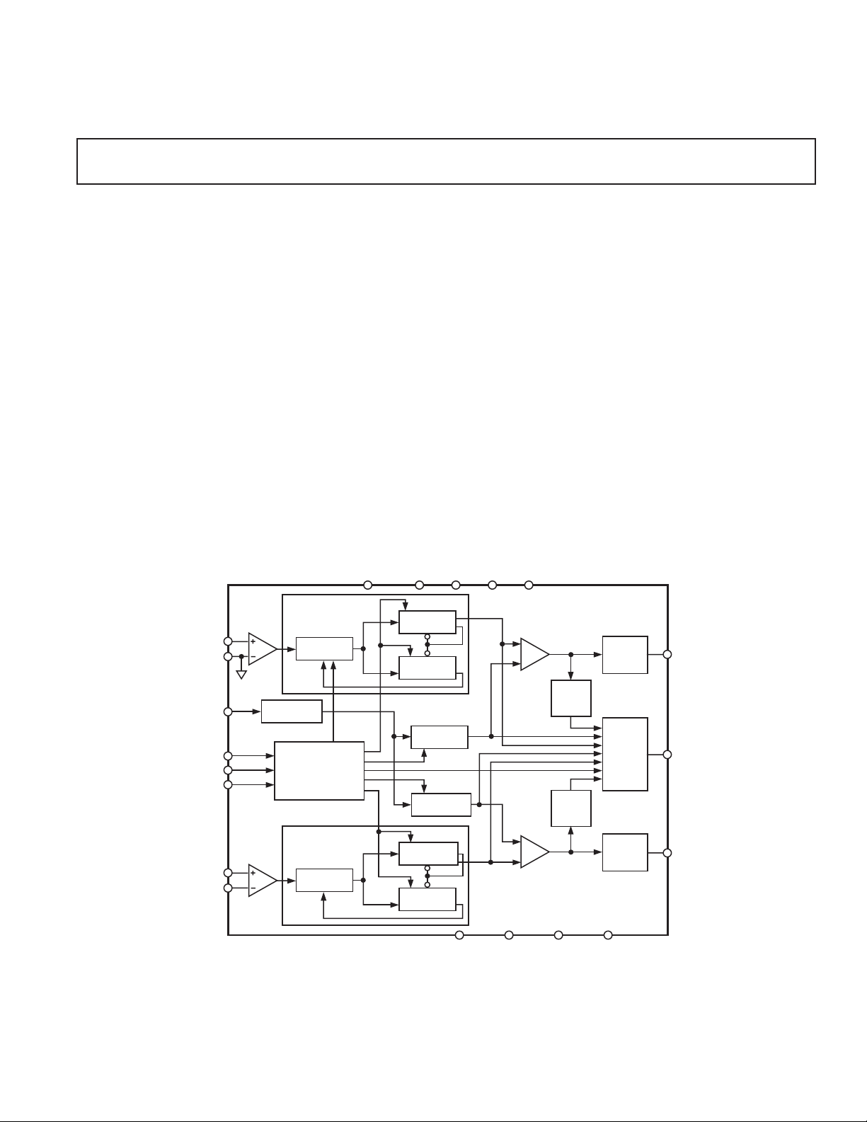
The ADF4217L/ADF4218L/ADF4219L are low power dual
frequency synthesizers that can be used to implement local
oscillators in the up-conversion and down-conversion sections
of wireless receivers and transmitters. They can provide the LO
for both the RF and IF sections. They consist of a low noise
digital PFD (phase frequency detector), a precision charge pump,
programmable reference divider, programmable A and B counters,
and a dual modulus prescaler (P/P + 1). The A and B counters,
in conjunction with the dual modulus prescaler
(P/P + 1),
implement an N divider (N = BP + A). In addition, the 14-bit
reference counter (R Counter) allows selectable REFIN
quencies at the PFD input. A complete PLL (phase-locked
loop) can be implemented if the synthesizers are used with an
external loop filter and VCOs (voltage controlled oscillators).
Control of all the on-chip registers is via a simple 3-wire interface
with 1.8 V compatibility. The devices operate with a power supply
ranging from 2.6 V to 3.3 V and can be powered down when
not in use.
fre-
a
REV. C
IF
IN
IF
IN
ADF4217L
ADF4218L
ONLY
REF
CLOCK
DATA
LE
RF
IN
RF
IN
FUNCTIONAL BLOCK DIAGRAM
ADF4219L ONLY
N = BP + A
A
B
IN
A
B
FEATURES IN ( ) REFER TO ADF4219L
NC = NO CONNECT
BUFFER
PRESCALER
22-BIT
DATA
REGISTER
N = BP + A
PRESCALER
IF
SDOUT
RF
NC
11(13)-BIT IF
B COUNTER
6(5)-BIT IF
A COUNTER
14(15)-BIT IF
R COUNTER
14(15)-BIT RF
R COUNTER
11(13)-BIT RF
B COUNTER
6(5)-BIT RF
A COUNTER
DGND
VP2VP1VDD2VDD1
PHASE
COMPARATOR
DETECT
DETECT
PHASE
COMPARATOR
AGNDRFDGNDIFAGND
RF
IF
LOCK
RF
LOCK
ADF4217L/
ADF4218L/
ADF4219L
CHARGE
PUMP
OUTPUT
MUX
CHARGE
PUMP
IF
CP
IF
MUXOUT
CP
RF
Information furnished by Analog Devices is believed to be accurate and
reliable. However, no responsibility is assumed by Analog Devices for its
use, nor for any infringements of patents or other rights of third parties that
may result from its use. No license is granted by implication or otherwise
under any patent or patent rights of Analog Devices. Trademarks and
registered trademarks are the property of their respective companies.
One Technology Way, P.O. Box 9106, Norwood, MA 02062-9106, U.S.A.
Tel: 781/329-4700 www.analog.com
Fax: 781/326-8703 © 2003 Analog Devices, Inc. All rights reserved.

ADF4217L/ADF4218L/ADF4219L–SPECIFICATIONS
(VDD1 = VDD2 = 2.6 V to 3.3 V; VP1, VP2 = VDD to 5.5 V; AGND = DGND = 0 V; TA = T
MIN
to T
, unless otherwise noted.)
MAX
1
BChips
2
Parameter B Version1(T y p i c a l) U nit Test Conditions/Comments
RF CHARACTERISTICS Use a square wave for operation
below minimum frequency spec.
RF Input Frequency (RF
)
IN
ADF4217L, ADF4218L 0.15/3.0 0.15/3.0 GHz min/max –10 dBm minimum input signal
ADF4217L, ADF4218L 0.15/2.5 0.15/2.5 GHz min/max –15 dBm minimum input signal
ADF4219L 0.8/2.2 0.8/2.2 GHz min/max –20 dBm minimum input signal
RF Input Sensitivity
ADF4217L, ADF4218L –15/0 –15/0 dBm min/max
ADF4219L –20/0 –20/0 dBm min/max
IF Input Frequency (IF
)
IN
ADF4217L/ADF4218L 0.045/1.1 0.045/1.1 GHz min/max –15 dBm minimum input signal
ADF4219L P = 16/17 0.045/1.0 0.045/1.0 GHz min/max –10 dBm minimum input signal
ADF4219L P = 8/9 0.045/0.55 0.045/0.55 GHz min/max –10 dBm minimum input signal
IF Input Sensitivity –15/0 –15/0 dBm min/max
Maximum Allowable Prescaler
Output Frequency
3
188 188 MHz max
REFIN CHARACTERISTICS
Reference Input Frequency 10/110 10/110 MHz min/max For f < 10 MHz, use dc-coupled
square wave, (0 to V
DD
).
Reference Input Sensitivity 0.5 0.5 V p-p min AC-coupled. When dc-coupled,
DD
max.
0 to V
REFIN Input Capacitance 10 10 pF max (CMOS compatible)
REFIN Input Current ± 100 ± 100 µA max
PHASE DETECTOR
Phase Detector Frequency
4
56 56 MHz max
CHARGE PUMP
ICP Sink/Source
High Value 4 4 mA typ
Low Value 1 1 mA typ
Absolute Accuracy 1 1 % typ
Three-State Leakage Current 1 1 nA typ
I
CP
Sink and Source Current Matching 6 6 % max 0.5 V < V
I
CP
vs. V
CP
55% max 0.5 V < VCP < VP – 0.5, 0.1% typ
< VP – 0.5, 1% typ
CP
ICP vs. Temperature 2 2 % typ VCP = VP/2
LOGIC INPUTS
V
, Input High Voltage 1.4 1.4 V min
INH
, Input Low Voltage 0.6 0.6 V max
V
INL
I
C
, Input Current ± 1 ± 1 µA max
INH/IINL
, Input Capacitance 10 10 pF max
IN
Reference Input Current ±100 ± 100 µA max
LOGIC OUTPUTS
VOH, Output High Voltage VDD – 0.4 VDD – 0.4 V min IOH = 1 mA
VOL, Output Low Voltage 0.4 0.4 V max IOL = 1 mA
POWER SUPPLIES
1 2.6/3.3 2.6/3.3 V min/V max
V
DD
V
2V
DD
1, VP2V
V
P
(RF + IF)
I
DD
(RF only)
(IF only)
1 + IP2) 0.6 0.6 mA typ TA = 25°C
I
P (IP
5
5
5
1V
DD
1/5.5 V VDD1/5.5 V V min/V max
DD
DD
1
10 10 mA max 7.1 mA typ
77mA 4.7 mA typ
55mA 3.4 mA typ
Low Power Sleep Mode 1 1 µA typ
–2–
REV. C
ADF4217L/ADF4218L/ADF4219L
BChips
2
Parameter B Version1(T y p i c a l) U nit Test Conditions/Comments
NOISE CHARACTERISTICS
RF Phase Noise Floor
IF Phase Noise Floor
Phase Noise Performance
9
RF
10
RF
11
IF
12
IF
Spurious Signals Measured at Offset of f
9
RF
10
RF
11
IF
12
IF
NOTES
1
Operating temperature range is as follows: B Version: –40°C to +85°C.
2
The BChip specifications are given as typical values.
3
This is the maximum operating frequency of the CMOS counters. The prescaler value should be chosen to ensure that the RF input is divided down to a frequency
that is less than this value.
4
Guaranteed by design. Sample tested to ensure compliance.
5
This includes relevant IP.
6
V
= 3 V; P = 16/32; IFIN/RFIN for ADF4218L, ADF4219L = 540 MHz/900 MHz.
DD
7
The synthesizer phase noise floor is estimated by measuring the in-band phase noise at the output of the VCO and subtracting 20logN (where N is the N divider value).
8
The phase noise is measured with the EVAL-ADF421xEB1 Evaluation Board and the HP8562E Spectrum Analyzer. The spectrum analyzer provides the REFIN
for the synthesizer. (f
9
f
= 10 MHz; f
REFIN
10
f
= 10 MHz; f
REFIN
11
f
= 10 MHz; f
REFIN
12
f
= 10 MHz; f
REFIN
Specifications subject to change without notice.
7
= 10 MHz @ 0 dBm.)
REFOUT
= 30 kHz; Offset frequency = 1 kHz; fRF = 1.95 GHz; N = 65000; Loop B/W = 3 kHz
PFD
= 200 kHz; Offset frequency = 1 kHz; fRF = 900 MHz; N = 4500; Loop B/W = 20 kHz
PFD
= 30 kHz; Offset frequency = 1 kHz; fIF = 900 MHz; N = 30000; Loop B/W = 3 kHz
PFD
= 200 kHz; Offset frequency = 1 kHz; fIF = 900 MHz; N = 4500; Loop B/W = 20 kHz
PFD
6
7
–171 –171 dBc/Hz typ @ 30 kHz PFD Frequency
–163 –163 dBc/Hz typ @ 200 kHz PFD Frequency
–167 –167 dBc/Hz typ @ 30 kHz PFD Frequency
8
–159 –159 dBc/Hz typ @ 200 kHz PFD Frequency
@ VCO Output
–75 –75 dBc/Hz typ 1.95 GHz Output; 30 kHz PFD
–90 –90 dBc/Hz typ 900 MHz Output; 200 kHz PFD
–77 –77 dBc/Hz typ 900 MHz Output; 30 kHz PFD
–86 –86 dBc/Hz typ 900 MHz Output; 200 kHz PFD
/2f
PFD
PFD
–78/–85 –78/–85 dBc typ
–80/–84 –80/–84 dBc typ
–79/–86 –79/–86 dBc typ
–80/–84 –80/–84 dBc typ
TIMING CHARACTERISTICS
VP2 ≤ 6.0 V ; AGND
RF1
= DGND
= AGND
RF1
(VDD1 = VDD2 = 3 V ⴞ 10%, 5 V ⴞ 10%; VDD1, VDD2 ≤ VP1,
= DGND
RF2
= 0 V; TA = T
RF2
MIN
to T
, unless otherwise noted.)
MAX
Limit at
to T
T
MIN
MAX
Parameter (B Version) Unit Test Conditions/Comments
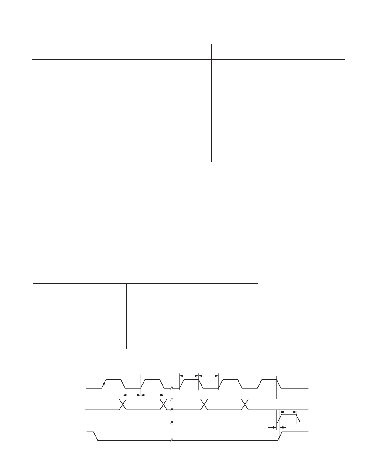
t
1
t
2
t
3
t
4
t
5
t
6
Guaranteed by design but not production tested.
10 ns min DATA to CLOCK Setup Time
10 ns min DATA to CLOCK Hold Time
25 ns min CLOCK High Duration
25 ns min CLOCK Low Duration
10 ns min CLOCK to LE Setup Time
50 ns min LE Pulsewidth
CLOCK
DATA
t
1
DB21 (MSB) DB20 DB2
LE
LE
t
2
t
t
3
4
(CONTROL BIT C2)
DB1
DB0 (LSB)
(CONTROL BIT C1)
t
5
t
6
REV. C
Figure 1. Timing Diagram
–3–
ADF4217L/ADF4218L/ADF4219L
ABSOLUTE MAXIMUM RATINGS
(
TA = 25°C, unless otherwise noted.)
VDD1 to GND3 . . . . . . . . . . . . . . . . . . . . . . –0.3 V to +3.6 V
VDD1 to VDD2 . . . . . . . . . . . . . . . . . . . . . . . –0.3 V to +0.3 V
1, VP2 to GND . . . . . . . . . . . . . . . . . . . . –0.3 V to +5.8 V
V
P
1, VP2 to VDD1 . . . . . . . . . . . . . . . . . . . . –0.3 V to +5.5 V
V
P
Digital I/O Voltage to GND . . . . . . . . –0.3 V to VDD + 0.3 V
Analog I/O Voltage to GND . . . . . . . . . –0.3 V to V
, RF1IN (A, B), IFIN (A, B)
REF
IN
to GND . . . . . . . . . . . . . . . . . . . . . . –0.3 V to VDD + 0.3 V
A to RFINB . . . . . . . . . . . . . . . . . . . . . . . . . . . ± 320 mV
RF
IN
Operating Temperature Range
Industrial (B Version) . . . . . . . . . . . . . . . –40°C to +85°C
Storage Temperature Range . . . . . . . . . . . . –65°C to +150°C
Maximum Junction Temperature . . . . . . . . . . . . . . . . 150°C
1, 2
+ 0.3 V
P
TSSOP
LGA
Thermal Impedance . . . . . . . . . . . . . 150.4°C/W
JA
. . . . . . . . . . . . . . . . . . . . . . . . . . . . . . . . . . 112°C/W
JA
Lead Temperature, Soldering
TSSOP, Vapor Phase (60 sec) . . . . . . . . . . . . . . . . . 215°C
TSSOP, Infrared (15 sec) . . . . . . . . . . . . . . . . . . . . 220°C
LGA, Vapor Phase (60 sec) . . . . . . . . . . . . . . . . . . . 240°C
LGA, Infrared (20 sec) . . . . . . . . . . . . . . . . . . . . . . . 240°C
NOTES
1
Stresses above those listed under Absolute Maximum Ratings may cause
nent damage to the device. This is a stress rating only; functional operation
device at these or any other conditions above those listed in the operational
of this specification is not implied. Exposure to absolute maximum rating
for extended periods may affect device reliability.
2
This device is a high performance RF integrated circuit with an ESD rating of
< 2 kV and is ESD sensitive. Proper precautions should be taken for handling
assembly.
3
GND = AGND = DGND = 0 V.
ORDERING GUIDE
Temperature Package Package
Model Range Description Option
ADF4217L/ADF4218L/ADF4219LBRU –40°C to +85°CThin Shrink Small Outline Package (TSSOP) RU-20
ADF4217L/ADF4218L/ADF4219LBCC –40°C to +85°CChip Array CASON (LGA) CC-24
*Contact the factory for chip availability.
sections
conditions
*
perma-
of the
and
CAUTION
ESD (electrostatic discharge) sensitive device. Electrostatic charges as high as 4000 V readily accumulate
on the human body and test equipment and can discharge without detection. Although the ADF4217L/
ADF4218L/ADF4219L feature proprietary ESD protection circuitry, permanent damage may occur on
devices subjected to high energy electrostatic discharges. Therefore, proper ESD precautions are
recommended to avoid performance degradation or loss of functionality.
–4–
REV. C
ADF4217L/ADF4218L/ADF4219L
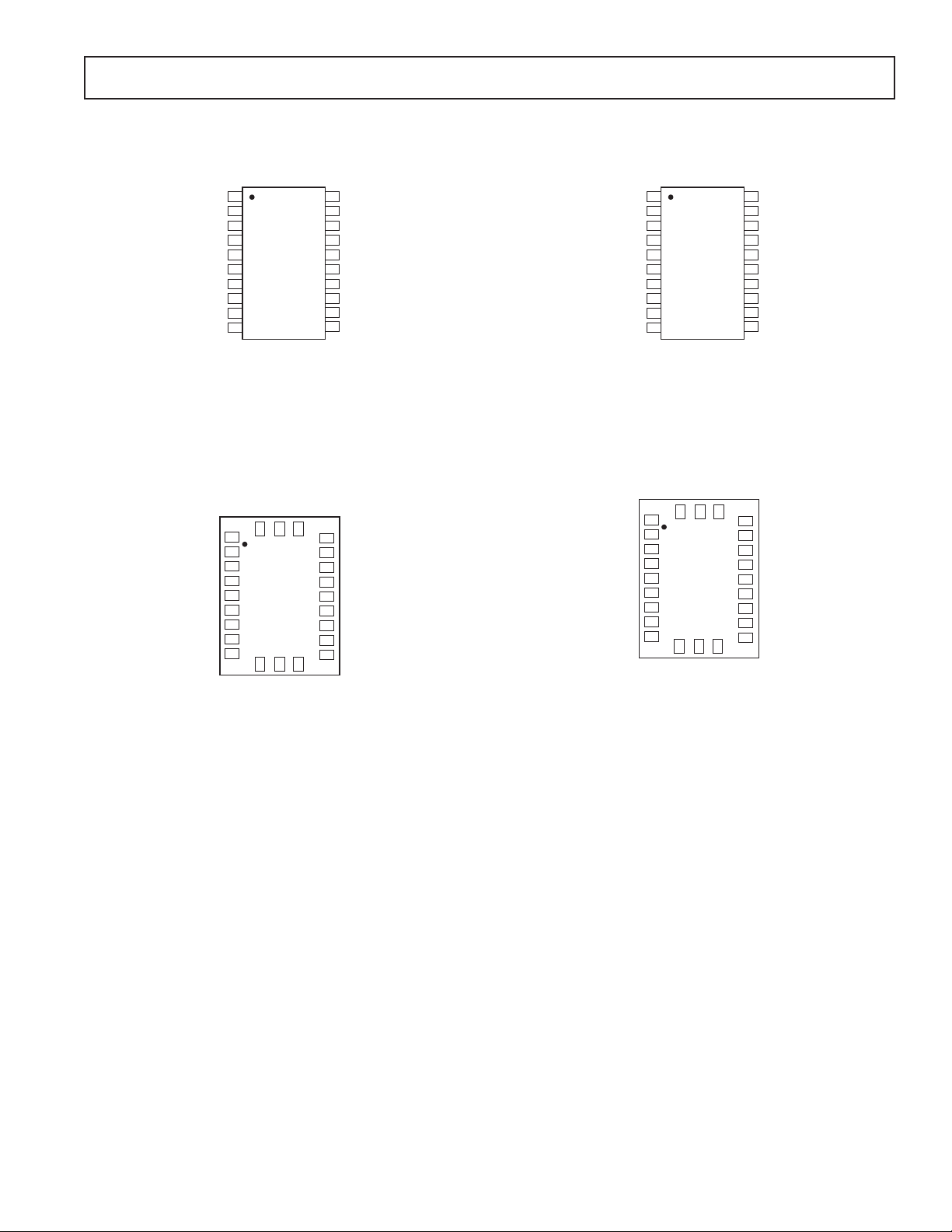
PIN CONFIGURATIONS
TSSOP
1
V
1
DD
V
1
2
P
CP
3
RF
DGND
AGND
MUXOUT
RF
RFINB
REF
DGND
IN
RF
A
RF
IN
IF
4
5
6
7
8
9
10
ADF4217L/
ADF4218L
CHIP SCALE
1
2
DD
V
V
23 22
24
1
2
VP1
3
CP
RF
DGND
AGND
4
RF
ADF4217L/
5
RF
A
IN
RFINB
REF
NC
ADF4218L
6
7
RF
8
IN
9
10
11 12
IF
DGND
MUXOUT
NC = NO INTERNAL CONNECT
TSSOP
1
20
VDD2
19
VP2
18
CP
IF
17
DGND
IF
16
IF
INA
15
IF
INB
14
AGND
IF
13
LE
12
DATA
11
CLK
V
DD
V
CP
DGND
RF
IN
RFINB
AGND
REF
DGND
MUXOUT
1
1
2
P
3
RF
4
RF
A
5
ADF4219L
6
7
RF
8
IN
9
IF
10
20
19
18
17
16
15
14
13
12
11
V
DD
VP2
CP
IF
DGND
IF
IN
AGND
NC
LE
DATA
CLK
2
IF
IF
CHIP SCALE
1
2
2
DD
P
DD
V
V
2
P
DD
V
21
NCNC
20
CP
IF
DGND
19
18
17
16
15
14
13
IFINA
IFINB
AGND
LE
DATA
NC
IF
IF
DGND
AGND
NC
VP1
CP
RF
IN
RFINB
REF
NC
1
2
3
RF
4
RF
ADF4219L
A
5
6
7
RF
8
IN
9
10
CLK
NC = NO INTERNAL CONNECT
24
IF
DGND
23 22
11 12
MUXOUT
V
CLK
21
NC
CP
20
IF
19
DGND
IF
IF
18
IN
AGND
17
16
15
14
13
IF
NC
LE
DATA
NC
REV. C
–5–

ADF4217L/ADF4218L/ADF4219L
PIN FUNCTION DESCRIPTIONS
Mnemonic Function
V
1Positive Power Supply for the RF Section. Decoupling capacitors to the analog ground plane should be placed as
DD
close as possible to this pin. V
potential as V
V
1Power Supply for the RF Charge Pump. This should be greater than or equal to VDD.
P
CP
RF
Output from the RF Charge Pump. When enabled, this provides ±ICP to the external loop filter, which in turn
DD
2.
drives the external VCO.
DGND
RF
RF
RF
A Input to the RF Prescaler. This low level input signal is normally ac-coupled to the external VCO.
IN
BComplementary Input to the RF Prescaler. This point should be decoupled to the ground plane with a small
IN
Ground Pin for the RF Digital Circuitry
bypass capacitor, typically 100 pF.
AGND
REF
IN
RF
Ground Pin for the RF Analog Circuitry
Reference Input. This is a CMOS input with a nominal threshold of VDD/2 and an equivalent input resistance of
100 kΩ. This input can be driven from a TTL or CMOS crystal oscillator, or can be ac-coupled.
DGND
IF
Ground Pin for the IF Digital, Interface, and Control Circuitry
MUXOUT This multiplexer output allows either the IF/RF Lock Detect, the scaled RF, or the scaled Reference Frequency to
be accessed externally (Table V).
CLK Serial Clock Input. This serial clock is used to clock in the serial data to the registers. The data is latched into the
22-bit shift register on the CLK rising edge. This input is a high impedance CMOS input.
DATA Serial Data Input. The serial data is loaded MSB first with the two LSBs being the control bits. This input is a
high impedance CMOS input.
LE Load Enable, CMOS Input. When LE goes high, the data stored in the shift registers is loaded into one of the four
latches; the latch is selected using the control bits.
AGND
IF
Ground Pin for the IF Analog Circuitry
NC This pin is not connected internally (ADF4219L only).
IF
BComplementary Input to the IF Prescaler. This point should be decoupled to the ground plane with a small bypass
IN
capacitor, typically 100 pF (ADF4217L/ADF4218L only).
IF
A Input to the IF Prescaler. This low level input signal is normally ac-coupled to the external VCO.
IN
DGND
CP
IF
IF
Ground Pin for the IF Digital, Interface, and Control Circuitry
Output from the IF Charge Pump. When enabled, this provides ±ICP to the external loop filter, which in turn drives
the external VCO.
V
2Power Supply for the IF Charge Pump. This should be greater than or equal to VDD.
P
V
2Positive Power Supply for the IF Interface and Oscillator Sections. Decoupling capacitors to the analog ground
DD
plane should be placed as close as possible to this pin. VDD2 should have a value of between 2.6 V and 3.3 V.
VDD2 must have the same potential as VDD1.
1 should have a value of between 2.6 V and 3.3 V. VDD1 must have the same
DD
–6–
REV. C
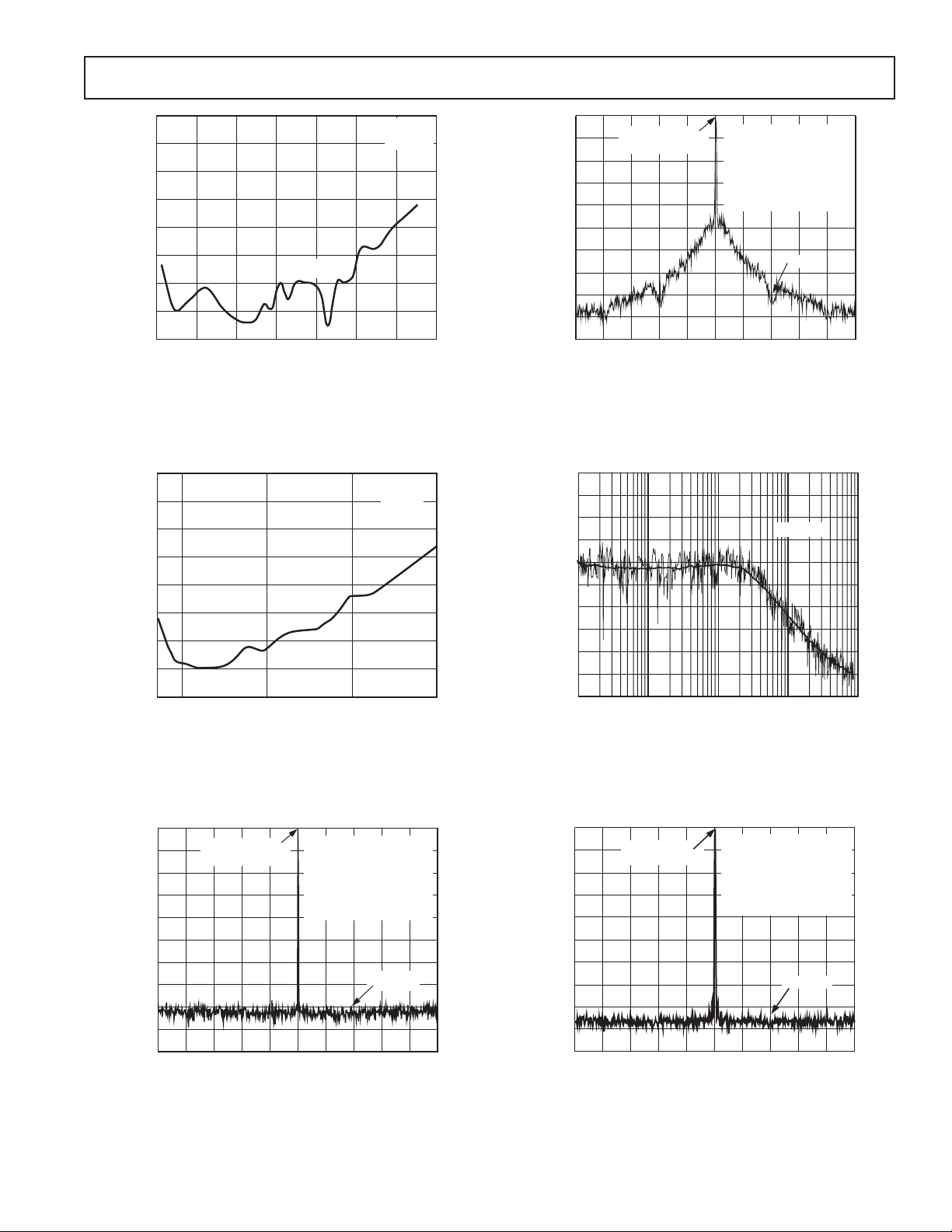
Typical Performance Characteristics–
ADF4217L/ADF4218L/ADF4219L
0
–5
–10
–15
–20
–25
RF INPUT POWER – dBm
–30
–35
–40
0 0.5 1.5 2.51.0 2.0 3.0
RF INPUT FREQUENCY – GHz
TA = 25ⴗC
TPC 1. Input Sensitivity, RF Input
0
–5
–10
–15
–20
–25
IF INPUT POWER – dBm
–30
–35
–40
0.1 0.6 1.1 1.6
IF INPUT FREQUENCY – GHz
V
= 3V
DD
V
= 3V
P
3.5
–10
–20
–30
–40
–50
–60
–70
OUTPUT POWER – dB
–80
–90
–100
0
–400kHz
REFERENCE
LEVEL = –11.2dBm
–200kHz 1960MHz 200kHz 400kHz
VDD = 3V, VP = 5V
= 4mA
I
CP
PFD FREQUENCY = 200kHz
RES. BANDWIDTH = 1kHz
VIDEO BANDWIDTH = 1kHz
SWEEP = 2.5 SECONDS
AVERAGES = 10
FREQUENCY
–78dBc
TPC 4. Reference Spurs, RF Side
(1960 MHz, 200 kHz, 20 kHz)
10dB/DIVISION RL = –40dBc/Hz rms NOISE = 1.2ⴗ
V
= 3V
DD
V
= 3V
P
–40
–50
–60
–70
–80
–90
–100
–110
PHASE NOISE – dBc/Hz
–120
–130
–140
100Hz FREQUENCY OFFSET FROM 1960MHz CARRIER 1MHz
1.2ⴗ rms
TPC 2. Input Sensitivity, IF Input
0
–10
–20
–30
–40
–50
–60
–70
OUTPUT POWER – dB
–80
–90
–100
REFERENCE
LEVEL = –11.2dBm
–2kHz –1kHz 1960MHz 1kHz 2kHz
VDD = 3V, VP = 5V
ICP = 4.0mA
PFD FREQUENCY = 200kHz
RES. BANDWIDTH = 10Hz
VIDEO BANDWIDTH = 10Hz
SWEEP = 1.9 SECONDS
AVERAGES = 20
FREQUENCY
–83dBc/Hz
TPC 3. Phase Noise, RF Side (1960 MHz, 200 kHz, 20 kHz)
REV. C
TPC 5. Integrated Phase Noise, RF Side
(1960 MHz, 200 kHz, 20 kHz)
0
–10
–20
–30
–40
–50
–60
–70
OUTPUT POWER – dB
–80
–90
–100
REFERENCE
LEVEL = –4.2dBm
–2kHz –1kHz 900MHz 1kHz 2kHz
V
= 3V, VP = 5V
DD
= 4mA
I
CP
PFD FREQUENCY = 200kHz
RES. BANDWIDTH = 10Hz
VIDEO BANDWIDTH = 10Hz
SWEEP = 1.9 SECONDS
AVERAGES = 20
FREQUENCY
–87dBc/Hz
TPC 6. Phase Noise, IF Side (900 MHz, 200 kHz, 20 kHz)
–7–
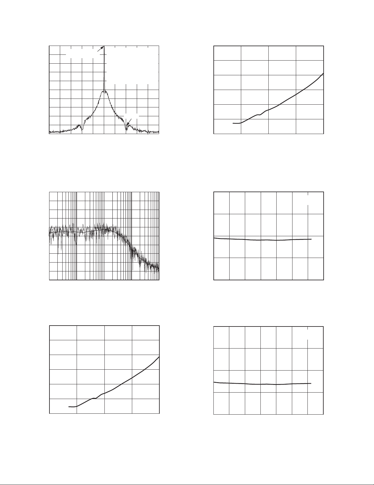
ADF4217L/ADF4218L/ADF4219L
0
–10
–20
–30
–40
–50
–60
–70
OUTPUT POWER – dB
–80
–90
–100
REFERENCE
LEVEL = –4.2dBm
–400kHz –200kHz 900MHz 200kHz 400kHz
VDD = 3V, VP = 5V
ICP = 4.0mA
PFD FREQUENCY = 200kHz
LOOP BANDWIDTH = 20kHz
RES. BANDWIDTH = 10kHz
VIDEO BANDWIDTH = 10kHz
SWEEP = 1.9 SECONDS
AVERAGES = 20
FREQUENCY
–83dBc
TPC 7. Reference Spurs, IF Side
(900 MHz, 200 kHz, 20 kHz)
10dB/DIVISION RL = –40dBc/Hz rms NOISE = 0.9ⴗ
–40
–50
–60
–70
–80
–90
–100
–110
PHASE NOISE – dBc/Hz
–120
–130
–140
100Hz FREQUENCY OFFSET FROM 900MHz CARRIER 1MHz
TPC 8. Integrated Phase Noise, IF Side
(900 MHz, 200 kHz, 20 kHz)
–120
–130
–140
–150
–160
PHASE NOISE – dBc/Hz
–170
–180
1 10000100 1000
10
PHASE DETECTOR FREQUENCY – kHz
V
= 3V
DD
= 5V
V
P
TPC 10. Phase Noise Referred to CP Output vs.
PFD Frequency, IF Side
–60
–70
–80
PHASE NOISE – dBc/Hz
–90
–100
–40 100–20
020406080
TEMPERATURE – ⴗC
VDD = 3V
= 5V
V
P
TPC 11. Phase Noise vs. Temperature, RF Side
(1960 MHz, 200 kHz, 20 kHz)
–120
–130
–140
–150
–160
PHASE NOISE – dBc/Hz
–170
–180
1 10000100 1000
10
PHASE DETECTOR FREQUENCY – kHz
V
= 3V
DD
= 5V
V
P
TPC 9. Phase Noise Referred to CP Output vs.
PFD Frequency, RF Side
–8–
–60
–70
–80
PHASE NOISE – dBc/Hz
–90
–100
–40 100–20
020406080
TEMPERATURE – ⴗC
= 3V
V
DD
V
= 5V
P
TPC 12. Phase Noise vs. Temperature, IF Side
(900 MHz, 200 kHz, 20 kHz)
REV. C

ADF4217L/ADF4218L/ADF4219L
TO PFD
N = BP + A
LOAD
LOAD
MODULUS
CONTROL
FROM IF/RF
INPUT STAGE
11(13)-BIT
B COUNTER
6(5)-BIT
A COUNTER
PRESCALER
P/P+1
6
4
2
0
– mA
CP
I
–2
–4
–6
0 5.00.5
1.0 1.5 2.0 2.5 3.0 3.5 4.0 4.5
TPC 13. Charge Pump Output Characteristics
CIRCUIT DESCRIPTION
Reference Input Section
The reference input stage is shown in Figure 2. SW1 and SW2
are normally closed switches; SW3 is normally open. When
power-down is initiated, SW3 is closed and SW1 and SW2 are
opened. This ensures that there is no loading of the REF
IN
pin
on power-down.
POWER-DOWN
CONTROL
50k⍀
NC
NO
SW2
SW3
NC = NORMALLY CLOSED
NO = NORMALLY OPEN
BUFFER
TO R
COUNTER
REF
IN
NC
SW1
Figure 2. Reference Input Stage
IF/RF Input Stage
The IF/RF input stage is shown in Figure 3. It is followed by a
two-stage limiting amplifier to generate the CML clock levels
needed for the prescaler.
VP = 5V
= 4mA
I
CP
VCP – V
Prescaler
The dual modulus prescaler (P/P + 1), along with the A and
B counters, enables the large division ratio, N, to be realized
(N = BP + A). This prescaler, operating at CML levels, takes
the clock from the IF/RF input stage and divides it down to a
manageable frequency for the CMOS A and B counters. It is
based on a synchronous 4/5 core.
The prescaler is selectable. On the IF side, it can be set to either 8/9
(DB20 of the IF AB Counter Latch set to 0) or 16/17 (DB20 set
to 1). On the RF side of the ADF4217L/ADF4218L, it can be set
to 64/65 or 32/33. On the ADF4219L, the RF prescaler can be
set to 16/17 or 32/33. See Tables V, VI, VIII, and IX.
A AND B COUNTERS
The A and B CMOS counters combine with the dual modulus
prescaler to allow a wide ranging division ratio in the PLL feedback counter. The devices are guaranteed to work when the
prescaler output is 188 MHz or less. Typically they will work
with 250 MHz output from the prescaler.
REV. C
BIAS
GENERATOR
A
RF
IN
B
RF
IN
Figure 3. IF/RF Input Stage
1.6V
500⍀500⍀
AV
DD
AGND
Figure 4. Reference Input Stage, A and B Counters
–9–

ADF4217L/ADF4218L/ADF4219L
The A and B counters, in conjunction with the dual modulus
prescaler, make it possible to generate output frequencies that
are spaced only by the Reference Frequency divided by R. The
equation for the VCO frequency is as follows:
fPBAfR
=×
[]
VCO REF
f
= Output frequency of external voltage controlled oscillator
VCO
+
()
× /
IN
(VCO).
P = Preset modulus of dual modulus prescaler (8/9, 16/17, and
so on).
B = Preset divide ratio of binary 11-bit counter (ADF4217L/
ADF4218L), binary 13-bit counter (ADF4219L).
A = Preset divide ratio of binary 6-bit A counter (ADF4217L/
ADF4218L), binary 5-bit counter (ADF4219L).
f
=Output frequency of the external reference frequency
REF
IN
oscillator.
R = Preset divide ratio of binary 14-bit programmable reference
counter (1 to 16383). The ADF4219L has an R divide
of 15 bits.
R COUNTER
The 14-bit R counter allows the input reference frequency to be
divided down to produce the reference clock to the phase frequency
detector (PFD). Division ratios from 1 to 16,383 are allowed. The
extra R15 bit on the ADF4219L allows ratios from 1 to 32767.
PHASE FREQUENCY DETECTOR (PFD) AND CHARGE PUMP
The PFD takes inputs from the R counter and N counter and
produces an output proportional to the phase and frequency
difference between them. Figure 5 is a simplified schematic.
V
P
CHARGE
PUMP
CP
R DIVIDER
D1 Q1
U1
CLR1
UP
DELAY
ELEMENT
U3
HI
MUXOUT AND LOCK DETECT
The output multiplexer on the ADF4217L family allows the user
to access various internal points on the chip. The state of MUXOUT
is controlled by P3, P4, P11, and P12. See Tables IV and VII.
Figure 6 shows the MUXOUT section in block diagram form.
DV
DD
IF ANALOG LOCK DETECT
IF R COUNTER OUTPUT
IF N COUNTER OUTPUT
IF/RF ANALOG LOCK DETECT
RF R COUNTER OUTPUT
RF N COUNTER OUTPUT
RF ANALOG LOCK DETECT
MUX CONTROL
MUXOUT
DGND
Figure 6. MUXOUT Circuit
Lock Detect
MUXOUT can be programmed for analog lock detect. The
N-channel open-drain analog lock detect should be operated
with an external pull-up resistor of 10 kΩ nominal. When lock
has been detected, it is high with narrow low going pulses.
INPUT SHIFT REGISTER
The functional block diagram for the ADF4217L family is shown
on page 1. The main blocks include a 22-bit input shift register,
a 14-bit R counter, and an N counter. The N counter is comprised
of a 6-bit A counter and an 11-bit B counter for the ADF4217L
and
the ADF4218L. The 18-bit N counter on the ADF4219L
comprised of a 13-bit B counter and a 5-bit A counter. Data
is
is clocked into the 22-bit shift register on each rising edge of
CLK. The data is clocked in MSB first. Data is transferred from
the shift register to one of four latches on the rising edge of LE.
The destination latch is determined by the state of the two control bits (C2, C1) in the shift register. These are the two LSBs,
DB1 and DB0, as shown in the timing diagram of Figure 1. The
truth table for these bits is shown in Table I.
Table I. C2, C1 Truth Table
N DIVIDER
R DIVIDER
N DIVIDER
CP OUTPUT
CLR2
D2 Q2
U2
DOWN
CPGND
HI
Figure 5. PFD Simplified Schematic
Control Bits
C2 C1 Data Latch
00 IF R Counter
01 IF AB Counter (and Prescaler Select)
10 RF R Counter
11
RF AB Counter (and Prescaler Select)
–10–
REV. C

ADF4217L/ADF4218L/ADF4219L
Table II. ADF4217L/ADF4218L Family Latch Summary
IF REFERENCE COUNTER LATCH
IF
O
IF F
POWER-DOWN
O
RF F
IF LOCK
DETECT
THREE-STATE
IF
PRESCALER
DETECT
RF LOCK
THREE-STATE
CP
CP
IF
IF
GAIN
IF CP
IF PD
POLARITY
P1
NOT
USED
14-BIT REFERENCE COUNTER, R
CONTROL
BITS
DB0DB1DB2DB3DB4DB5DB6DB7DB8DB9DB10DB11DB12DB13DB14DB15DB16DB17DB18DB19DB20DB21
C1 (0)C2 (0)R1R2R3R4R5R6R7R8R9R10R11R12R13R14P5P2P3P4
IF AB COUNTER LATCH
11-BIT B COUNTER
NOT
USED
6-BIT A COUNTER
CONTROL
BITS
DB0DB1DB2DB3DB4DB5DB6DB7DB8DB9DB10DB11DB12DB13DB14DB15DB16DB17DB18DB19DB20DB21
C1 (1)C2 (0)A1A2A3A4A5A6B1B2B3B4B5B6B7B8B9B10B11P6P7
RF REFERENCE COUNTER LATCH
GAIN
RF CP
RF PD
POLARITY
NOT
USED
14-BIT REFERENCE COUNTER, R
CONTROL
BITS
DB0DB1DB2DB3DB4DB5DB6DB7DB8DB9DB10DB11DB12DB13DB14DB15DB16DB17DB18DB19DB20DB21
C1 (0)C2 (1)R1R2R3R4R5R6R7R8R9R10R11R12R13R14P13P10P11P12 P9
RF AB COUNTER LATCH
RF
POWER-DOWN
RF
PRESCALER
11-BIT B COUNTER
NOT
USED
6-BIT A COUNTER
CONTROL
BITS
DB0DB1DB2DB3DB4DB5DB6DB7DB8DB9DB10DB11DB12DB13DB14DB15DB16DB17DB18DB19DB20DB21
C1 (1)C2 (1)A1A2A3A4A5A6B1B2B3B4B5B6B7B8B9B10B11P14P16
REV. C
–11–

ADF4217L/ADF4218L/ADF4219L
Table III. ADF4219L Family Latch Summary
IF REFERENCE COUNTER LATCH
IF
O
IF F
POWER-DOWN
O
RF F
IF LOCK
DETECT
THREE-STATE
IF
PRESCALER
DETECT
RF LOCK
THREE-STATE
P10P11P12
CP
CP
IF
GAIN
IF CP
IF PD
POLARITY
R15
P1
15-BIT REFERENCE COUNTER, R
CONTROL
BITS
DB0DB1DB2DB3DB4DB5DB6DB7DB8DB9DB10DB11DB12DB13DB14DB15DB16DB17DB18DB19DB20DB21
C1 (0)C2 (0)R1R2R3R4R5R6R7R8R9R10R11R12R13R14P5P2P3P4
IF AB COUNTER LATCH
13-BIT B COUNTER
5-BIT A COUNTER
CONTROL
BITS
DB0DB1DB2DB3DB4DB5DB6DB7DB8DB9DB10DB11DB12DB13DB14DB15DB16DB17DB18DB19DB20DB21
C1 (1)C2 (0)A1A2A3A4A5B1B2B3B4B5B6B7B8B9B10B11B12B13P6P7
RF REFERENCE COUNTER LATCH
IF
GAIN
RF CP
RF PD
POLARITY
P13
R15
P9
15-BIT REFERENCE COUNTER, R
CONTROL
BITS
DB0DB1DB2DB3DB4DB5DB6DB7DB8DB9DB10DB11DB12DB13DB14DB15DB16DB17DB18DB19DB20DB21
C1 (0)C2 (1)R1R2R3R4R5R6R7R8R9R10R11R12R13R14
RF
POWER-DOWN
RF
PRESCALER
RF AB COUNTER LATCH
13-BIT B COUNTER
5-BIT A COUNTER
CONTROL
BITS
DB0DB1DB2DB3DB4DB5DB6DB7DB8DB9DB10DB11DB12DB13DB14DB15DB16DB17DB18DB19DB20DB21
C1 (1)C2 (1)A1A2A3A4A5B1B2B3B4B5B6B7B8B9B10B11B12B13P14P16
–12–
REV. C

ADF4217L/ADF4218L/ADF4219L
Table IV. ADF4217L/ADF4218L/ADF4219L IF Reference Counter Latch Map
IF REFERENCE COUNTER LATCH
O
IF F
IF LOCK
DETECT
IF
CP
GAIN
IF CP
IF PD
ONLY
ADF4219L
THREE-STATE
P5
0
1
POLARITY
R15
P1 PD POLARITY
0
NEGATIVE
1
POSITIVE
I
CP
1.0mA
4.0mA
14-BIT REFERENCE COUNTER, R
R14 R13 R12 .......... R3 R2 R1 DIVIDE RATIOR15
0
0
0
0
0
0
0
0
0
0
0
0
.
.
.
.
.
.
.
.
.
0
1
1
0
1
1
0
1
1
0
1
1
.
.
.
1
1
1
..........
0
..........
0
..........
0
..........
0
..........
.
..........
.
..........
.
..........
1
..........
1
..........
1
..........
1
..........
.
..........
1
0
0
0
1
0
1
1
0
.
.
.
.
.
.
1
0
1
0
1
1
1
1
.
.
1
1
CONTROL
BITS
DB0DB1DB2DB3DB4DB5DB6DB7DB8DB9DB10DB11DB12DB13DB14DB15DB16DB17DB18DB19DB20DB21
C1 (0)C2 (0)R1R2R3R4R5R6R7R8R9R10R11R12R13R14P1P5P2P3P4
1
1
2
0
3
1
4
0
.
.
.
.
.
.
16380
0
16381
1
16382
0
16383
1
.
.
32767
1
P2
01NORMAL
P12 P11
FROM RF R LATCH
0
0
0
0
0
0
1
1
1
1
1
1
0
0
X
X
1
1
X
X
0
0
1
1
CHARGE PUMP
OUTPUT
THREE-STATE
P4 P3 MUXOUT
0
0
1
1
0
0
0
0
1
1
1
1
0
1
0
1
0
1
0
1
0
1
0
1
LOGIC LOW STATE
IF ANALOG LOCK DETECT
IF REFERENCE DIVIDER OUTPUT
IF N DIVIDER OUTPUT
RF ANALOG LOCK DETECT
RF/IF ANALOG LOCK DETECT
RF REFERENCE DIVIDER
RF N DIVIDER
FA ST LOCK OUTPUT SWITCH ON
AND CONNECTED TO MUXOUT
IF COUNTER RESET
RF COUNTER RESET
IF AND RF COUNTER RESET
REV. C
–13–

ADF4217L/ADF4218L/ADF4219L
Table V. ADF4217L/ADF4218L IF AB Counter Latch Map
IF AB COUNTER LATCH
IF
POWER-DOWN
IF
PRESCALER
B11 B10 B9 .......... B3 B2 B1 B COUNTER DIVIDE RATIO
0
0
0
0
0
0
.
.
.
.
.
.
1
1
1
1
1
1
1
1
11-BIT B COUNTER
0
0
0
.
.
.
1
1
1
1
..........
..........
..........
..........
..........
..........
..........
..........
..........
..........
0
0
0
0
.
.
.
1
1
1
1
1
1
0
1
1
.
.
.
.
.
.
0
0
0
1
1
0
1
1
NOT
USED
A6
A5 A4 A3 A2 A1 A COUNTER DIVIDE RATIO
0
0
0
0
0
0
0
0
.
.
.
.
.
.
1
1
1
1
NOT ALLOWED
NOT ALLOWED
3
.
.
.
2044
2045
2046
2047
6-BIT A COUNTER
0
0
0
0
0
0
0
0
.
.
.
1
1
0
0
1
0
1
.
.
.
.
.
.
1
1
1
1
0
1
1
0
2
1
3
.
.
.
.
.
.
0
62
1
63
CONTROL
BITS
DB0DB1DB2DB3DB4DB5DB6DB7DB8DB9DB10DB11DB12DB13DB14DB15DB16DB17DB18DB19DB20DB21
C1 (1)C2 (0)A1A2A3A4A5A6B1B2B3B4B5B6B7B8B9B10B11P6P7
P6 IF PRESCALER
0
8/9
1
16/17
P7 IF SECTION
0
NORMAL OPERATION
1
POWER-DOWN
N = BP + A, P IS PRESCALER VALUE SET BY P6. B MUST BE
GREATER THAN OR EQUAL TO A. TO ENSURE CONTINUOUSLY
ADJACENT VALUES OF N, N
IS (P2 – P).
MIN
–14–
REV. C

ADF4217L/ADF4218L/ADF4219L
Table VI. ADF4219L IF AB Counter Latch Map
IF AB COUNTER LATCH
IF
POWER-DOWN
IF
PRESCALER
B13 B12 B11 .......... B3 B2 B1 B COUNTER DIVIDE RATIO
0
0
0
0
.
.
.
1
1
1
1
0
0
0
0
0
.
.
.
.
.
.
1
1
1
1
1
1
1
1
13-BIT B COUNTER
..........
..........
..........
..........
..........
..........
..........
..........
..........
..........
A5 A4 A3 A2 A1 A COUNTER DIVIDE RATIO
0
0
0
0
0
.
1
1
0
0
0
0
.
.
.
1
1
1
1
1
1
0
1
1
.
.
.
.
.
.
0
0
0
1
1
0
1
1
0
0
0
0
0
0
0
.
.
1
1
1
1
NOT ALLOWED
NOT ALLOWED
3
.
.
.
8188
8189
8190
8191
5-BIT A COUNTER
0
0
1
1
.
1
1
CONTROL
BITS
DB0DB1DB2DB3DB4DB5DB6DB7DB8DB9DB10DB11DB12DB13DB14DB15DB16DB17DB18DB19DB20DB21
C1 (1)C2 (0)A1A2A3A4A5B1B2B3B4B5B6B7B8B9B10B11B12B13P6P7
0
1
0
1
.
0
1
0
1
2
3
.
30
31
REV. C
P6 IF PRESCALER
0
8/9
1
16/17
P7 IF SECTION
0
NORMAL OPERATION
1
POWER-DOWN
N = BP + A, P IS PRESCALER VALUE SET BY P6.
B MUST BE GREATER THAN OR EQUAL TO A.
FOR CONTIGUOUS VALUES OF N, N
–15–
IS (P2– P).
MIN

ADF4217L/ADF4218L/ADF4219L
Table VII. RF Reference Counter Latch Map
RF REFERENCE COUNTER LATCH
O
RF F
DETECT
RF LOCK
IF
CP
GAIN
RF CP
THREE-STATE
P9 PD POLARITY
0
1
P13
0
1
RF PD
POLARITY
P9
I
CP
1.0mA
4.0mA
ONLY
ADF4129L
R15
NEGATIVE
POSITIVE
14-BIT REFERENCE COUNTER, R
R14 R13 R12 .......... R3 R2 R1 DIVIDE RATIOR15
0
0
0
0
0
0
0
0
0
0
0
0
.
.
.
.
.
.
.
.
.
0
1
1
0
1
1
0
1
1
0
1
1
.
.
.
1
1
1
..........
0
..........
0
..........
0
..........
0
..........
.
..........
.
..........
.
..........
1
..........
1
..........
1
..........
1
..........
.
..........
1
0
0
0
1
0
1
1
0
.
.
.
.
.
.
1
0
1
0
1
1
1
1
.
.
1
1
CONTROL
BITS
DB0DB1DB2DB3DB4DB5DB6DB7DB8DB9DB10DB11DB12DB13DB14DB15DB16DB17DB18DB19DB20DB21
C1 (0)C2 (1)R1R2R3R4R5R6R7R8R9R10R11R12R13R14P13P10P11P12
1
1
2
0
3
1
4
0
.
.
.
.
.
.
16380
0
16381
1
16382
0
16383
1
.
.
32767
1
P10
0
1
P12 P11
0
0
0
0
0
0
1
1
1
1
1
1
0
0
X
X
1
1
X
X
0
0
1
1
CHARGE PUMP
OUTPUT
NORMAL
THREE-STATE
P4 P3
FROM RF R LATCH
0
0
1
1
0
0
0
0
1
1
1
1
MUXOUT
LOGIC LOW STATE
0
IF ANALOG LOCK DETECT
1
IF REFERENCE DIVIDER OUTPUT
0
IF N DIVIDER OUTPUT
1
RF ANALOG LOCK DETECT
0
RF/IF ANALOG LOCK DETECT
1
RF REFERENCE DIVIDER
0
RF N DIVIDER
1
FA ST LOCK OUTPUT SWITCH ON
0
AND CONNECTED TO MUXOUT
IF COUNTER RESET
1
RF COUNTER RESET
0
IF AND RF COUNTER RESET
1
–16–
REV. C

ADF4217L/ADF4218L/ADF4219L
Table VIII. ADF4217L/ADF4218L RF AB Counter Latch Map
RF AB COUNTER LATCH
RF
POWER-DOWN
RF
PRESCALER
B11 B10 B9 .......... B3 B2 B1 B COUNTER DIVIDE RATIO
0
0
0
0
0
0
0
0
.
.
.
.
.
.
1
1
1
1
1
1
1
1
11-BIT B COUNTER
..........
0
..........
0
..........
0
..........
0
..........
.
..........
.
..........
.
..........
1
..........
1
..........
1
..........
1
0
0
0
0
1
.
.
.
1
1
1
1
1
1
0
1
1
0
0
.
.
.
.
.
.
0
0
0
1
1
0
1
1
NOT
USED
A6
A5 A4 A3 A2 A1 A COUNTER DIVIDE RATIO
0
0
0
0
0
0
0
0
.
.
.
.
.
.
1
1
1
1
NOT ALLOWED
NOT ALLOWED
3
4
.
.
.
2044
2045
2046
2047
6-BIT A COUNTER
0
0
0
0
0
0
0
0
.
.
.
1
1
0
0
1
0
1
.
.
.
.
.
.
1
1
1
1
0
1
1
0
2
1
3
.
.
.
.
.
.
0
62
1
63
CONTROL
BITS
DB0DB1DB2DB3DB4DB5DB6DB7DB8DB9DB10DB11DB12DB13DB14DB15DB16DB17DB18DB19DB20DB21
C1 (1)C2 (1)A1A2A3A4A5A6B1B2B3B4B5B6B7B8B9B10B11P14P16
REV. C
RF PRESCALER
P14
ADF4217L
0
64/65
1
32/33
P16 RF SECTION
0
NORMAL OPERATION
1
POWER-DOWN
RF PRESCALER
ADF4218L
32/33
64/65
N = BP + A, P IS PRESCALER VALUE SET BY P6, B MUST BE
GREATER THAN OR EQUAL TO A. TO ENSURE CONTINUOUSLY
ADJACENT VALUES OF NⴛF
REF
, N
IS (P2– P).
MIN
–17–

ADF4217L/ADF4218L/ADF4219L
Table IX. ADF4219L RF AB Counter Latch Map
RF AB COUNTER LATCH
RF
POWER-DOWN
RF
PRESCALER
B13 B12 B11 .......... B3 B2 B1
0
0
0
0
0
.
.
.
1
1
1
1
0
0
0
0
0
0
0
.
.
.
.
.
.
1
1
1
1
1
1
1
1
13-BIT B COUNTER
..........
..........
..........
..........
..........
..........
..........
..........
..........
..........
..........
0
0
0
1
.
.
.
1
1
1
1
5-BIT A COUNTER
A5 A4 A3 A2 A1 A COUNTER DIVIDE RATIO
0
0
0
0
0
0
0
0
0
0
0
0
.
.
1
1
1
1
B COUNTER DIVIDE RATIO
0
1
1
0
.
.
.
0
0
1
1
NOT ALLOWED
1
NOT ALLOWED
0
3
1
4
0
.
.
.
.
.
.
8188
0
8189
1
8190
0
8191
1
0
0
1
0
1
.
.
1
1
1
1
0
1
1
0
2
1
3
.
.
0
30
1
31
CONTROL
BITS
DB0DB1DB2DB3DB4DB5DB6DB7DB8DB9DB10DB11DB12DB13DB14DB15DB16DB17DB18DB19DB20DB21
C1 (1)C2 (1)A1A2A3A4A5B1B2B3B4B5B6B7B8B9B10B11B12B13P14P16
P14 IF PRESCALER
0
16/17
1
32/33
P16 IF SECTION
0
NORMAL OPERATION
1
POWER-DOWN
–18–
N = BP + A, P IS PRESCALER VALUE SET BY P14.
B MUST BE GREATER THAN OR EQUAL TO A.
FOR CONTIGUOUS VALUES OF N, N
A MUST BE LESS THAN P.
IS (P2–P).
MIN
REV. C

ADF4217L/ADF4218L/ADF4219L
PROGRAM MODES
Tables IV and VII show how to set up the program modes in the
ADF4217L family. The following should be noted:
1. IF and RF Analog Lock Detect indicate when the PLL is in
lock. When the loop is locked, and either IF or RF Analog
Lock Detect is selected, the MUXOUT pin will show a logic
high with narrow low-going pulses. When the IF/RF Analog
Lock Detect is chosen, the locked condition is indicated only
when both IF and RF loops are locked.
2. The IF Counter Reset Mode resets the R and N counters in
the IF section and also puts the IF charge pump into threestate. The RF Counter Reset Mode resets the R and N counters
in the RF section and also puts the RF charge pump into
three-state. The IF and RF Counter Reset Mode does both
of the above.
Upon removal of the reset bits, the N counter resumes counting
in close alignment with the R counter (maximum error is one
prescaler output cycle).
3. The Fastlock Mode uses MUXOUT to switch a second loop
filter damping resistor to ground during Fastlock operation.
Activation of Fastlock occurs whenever RF CP Gain in the
RF Reference counter is set to 1.
POWER-DOWN
It is possible to program the ADF4217L family for either synchronous
or asynchronous power-down on either the IF or RF side.
Synchronous IF Power-Down
Programming a “1” to P7 of the ADF4217L family will initiate a
power-down. If P2 of the ADF4217L family has been set to “0”
(normal operation), then a synchronous power-down is conducted.
The device will automatically put the charge pump into threestate and then complete the power-down.
Asynchronous IF Power-Down
If P2 of the ADF4217L family has been set to “1” (three-state the
IF charge pump) and P7 is subsequently set to “1,” an asynchronous power-down is conducted. The device will go into power-down
on the rising edge of LE, which latches the “1” to the IF PowerDown Bit (P7).
Synchronous RF Power-Down
Programming a “1” to P16 of the ADF4217L family will initiate a
power-down. If P10 of the ADF4217L family has been set to
(normal operation), a synchronous power-down is conducted.
“0”
The
device will automatically put the charge pump into three-state
and then complete the power-down.
Asynchronous RF Power-Down
If P10 of the ADF4217L family has been set to “1” (three-state
the RF charge pump) and P16 is subsequently set to “1,” an
asynchronous power-down is conducted. The device will go into
power-down on the rising edge of LE, which latches the “1” to
the RF Power-Down Bit (P16).
Activation of either synchronous or asynchronous power-down
forces the IF/RF loop’s R and N dividers to their load state
conditions, and the IF/RF input section is debiased to a high
impedance state.
The REF
RF power-downs are set.
The input register and latches remain active and are capable of
loading and latching data during all the power-down modes.
The IF/RF section of the devices will return to normal powered-up
operation immediately upon LE latching a “0” to the
power-down bit.
IF SECTION
Programmable IF Reference (R) Counter
If control bits C2, C1 are 0, 0, then the data is transferred from
the input shift register to the 14-bit IF R counter. Table IV shows
the input shift register data format for the IF R counter and the
possible divide ratios.
IF Phase Detector Polarity
P1 sets the IF phase detector polarity. When the IF VCO
acteristics are positive, this should be set to “1.” When they are
negative, it should be set to “0.” See Table IV.
IF Charge Pump Three-State
P2 puts the IF charge pump into three-state mode when programmed
to a “1.” It should be set to “0” for normal operation. See Table IV.
IF Charge Pump Currents
P5 sets the IF charge pump current. With P5 set to “0,” ICP is
1.0 mA. With P5 set to “1,” I
Programmable IF AB Counter
If control bits C2, C1 are 0, 1, the data in the input register is
used to program the IF AB counter. For the ADF4217L/ADF4218L,
the AB counter consists of a 6-bit swallow counter (A counter)
and 11-bit programmable counter (B counter). Table V shows
the input register data format for programming the IF AB counter
and the possible divide ratios. The ADF4219L N
of an 13-bit B counter and 5-bit A counter. Table VI shows the
input register data format for programming the ADF4219L.
IF Prescaler Value
P6 in the IF AB counter latch sets the IF prescaler value. For
the ADF4217L family, 8/9 or 16/17 prescalers are available. See
Table V and Table VI.
IF Power-Down
Tables IV, V, and VI show the power-down bits in the ADF4217L
family. See the Power-Down section for a functional description.
RF SECTION
Programmable RF Reference (R) Counter
If control bits C2, C1 are 1, 0, the data is transferred from
input shift register to the 14-bit RF R counter. Table VII shows
input shift register data format for the RF R counter and the
possible divide ratios.
RF Phase Detector Polarity
P9 sets the RF phase detector polarity. When the RF VCO
characteristics are positive, this should be set to “1.” When they
are negative, it should be set to “0.” See Table VII.
RF Charge Pump Three-State
P10 puts the RF charge pump into three-state mode when programmed
to a “1.” It should be set to “0” for normal operation. See Table VII.
oscillator circuit is only disabled if both the IF and
IN
appropriate
char-
is 4.0 mA. See Table IV.
CP
counter consists
the
the
REV. C
–19–

ADF4217L/ADF4218L/ADF4219L
RF Program Modes
Tables IV and VII show how to set up the RF program modes.
RF Charge Pump Currents
P13 sets the RF charge pump current. With P13 set to “0,” ICP is
1.0 mA. With P13 set to “1,” I
is 4.0 mA. See Table VII.
CP
Programmable RF AB Counter
If control bits C2, C1 are 1, 1, the data in the input register is used
to program the RF AB counter. For the ADF4217L/ADF4218L,
the AB counter consists of a 6-bit swallow counter (A counter)
and 11-bit programmable counter (B counter). Table VIII shows
the input register data format for programming the RF AB counter
and the possible divide ratios. The ADF4219L N counter consists
of a 13-bit B counter and 5-bit A counter. Table IX shows the
input register data format for programming the ADF4219L.
RF Prescaler Value
P14 in the RF AB counter latch sets the RF prescaler value. For
the ADF4217L and ADF4218L family, 32/33 or 64/65 prescalers
are available. See Table VIII. For the ADF4219L, the prescaler
may be 16/17 or 32/33. See Table IX.
RF Power-Down
Tables VII, VIII, and IX show the power-down bits (Charge
Pump Bit used for asynchronous in the ADF4217L family). See
the Power-Down section for a functional description.
RF Fastlock
The RF CP Gain Bit (P13) of the RF N Register in the ADF4217L
family is the Fastlock Enable Bit. The loop filter should be
designed for the lower current setting. When Fastlock is enabled,
the RF CP current is set to maximum value. Also, an extra loop
filter damping resistor to ground is switched in using the
MUXOUT pin, thus compensating for the change of loop
dynamics when in Fastlock Mode. Since the RF CP Gain Bit is
contained in the RF N counter, only one write is needed to
program the new frequency and to initiate Fastlock. To come
out of Fastlock, the RF CP Gain Bit should be returned to “0”
and the extra damping resistor switched out.
APPLICATIONS SECTION
Local Oscillator for GSM Handset Receiver
The diagram in Figure 7 shows the ADF4217L/ADF4218L/
ADF4219L being used in a classic superheterodyne receiver to
provide the required LOs (local oscillators). In this circuit, the
reference input signal is applied to the circuit at f
being generated by a 13 MHz temperature controlled crystal
REF
and is
IN
oscillator. In order to have a channel spacing of 200 kHz (the GSM
standard), the reference input must be divided by 65, using the
on-chip reference counter.
The RF output frequency range is 1050 MHz to 1085 MHz.
Loop filter component values are chosen so that the loop bandwidth is 20 kHz. The synthesizer is set up for a charge pump
current of 4.0 mA, and the VCO sensitivity is 15.6 MHz/V.
The IF output is fixed at 125 MHz. The IF loop bandwidth is
chosen to be 20 kHz with a channel spacing of 200 kHz. Loop
filter component values are chosen accordingly.
Local Oscillator for WCDMA Receiver
Figure 8 shows the ADF4217L/ADF4218L/ADF4219L being
used to generate the local oscillator frequencies in a wideband
CDMA (WCDMA) system.
The RF output range needed is 1720 MHz to 1780 MHz. The
VCO190-1750T from Varil-L will accomplish that. Channel spacing
is 200 kHz, the loop bandwidth of the loop filter is 20 kHz, and the
VCO sensitivity is 32 MHz/V. A charge pump current of 4.0 mA
is used and the desired phase margin for the loop is 45 degrees.
The IF output is fixed at 200 MHz. The VCO190-200T is used.
It has a sensitivity of 11.5 MHz/V. Channel spacing and loop
bandwidth are chosen the same as the RF side.
100pF
18⍀
18⍀
100pF
18⍀
RF
OUT
18⍀
18⍀
IF
OUT
18⍀
100pF
V
CC
VCO190-125T
3.3k⍀
9k⍀
3.9nF
V
V
DD
P
CP
IF
400pF620pF
ADF4217L/
ADF4218L/
CP
V
P
VP1VP2VDD2VDD1
RF
620pF
3.3k⍀
5.8k⍀
6nF
620pF
V
VCO190-1068U
100pF
CC
ADF4219L
LOCK
DETECT
IN
CLK
SPI COMPATIBLE SERIAL BUS
LE
100pF
51⍀
51⍀
RF
RF
DGND
AGND
IF
DGND
AGND
MUXOUT
RF
IF
DATA
100pF
V
DD
10MHz
TCXO
DECOUPLING CAPACITORS (22F/10pF) ON VDD, VP OF THE ADF4217L/ADF4218L/ADF4219L.
THE TCXO AND ON V
OF THE VCOs HAVE BEEN OMITTED FROM THE DIAGRAM TO AID CLARITY.
CC
IF
REF
IN
IN
Figure 7. Local Oscillator Design for GSM Receiver
–20–
REV. C

ADF4217L/ADF4218L/ADF4219L
IF
100pF
18⍀
18⍀
OUT
18⍀
100pF
V
CC
VCO190-200T
3.3k⍀
1.5k⍀
24nF
2.4pF450pF
CP
V
P
IF
V
DD
ADF4217L/
ADF4218L/
ADF4219L
51⍀
100pF
10MHz
TCXO
DECOUPLING CAPACITORS (22F/10pF) ON VDD, VP OF THE ADF4217L/ADF4218L/ADF4219L.
THE TCXO AND ON V
OF THE VCOs HAVE BEEN OMITTED FROM THE DIAGRAM TO AID CLARITY.
CC
IF
REF
IN
RF
IF
RF
IN
DGND
AGND
DGND
Figure 8. Local Oscillator Design for WCDMA System
In this circuit, the reference input signal is applied to the circuit
at REFIN by a 10 MHz TCXO (temperature controlled crystal
oscillator).
INTERFACING
The ADF4217L/ADF4218L/ADF4219L family has a simple
®
SPI
compatible serial interface for writing to the device. SCLK,
SDATA, and LE control the data transfer. When LE (latch
enable) goes high, the 22 bits that have been clocked into the
input register on each rising edge of SCLK will get transferred
to the appropriate latch. See Figure 1 for the timing diagram
and Table I for the latch truth table.
The maximum allowable serial clock rate is 20 MHz. This means
that the maximum update rate possible for the device is 909 kHz
or one update every 1.1 µs. This is certainly more than adequate
for systems that will have typical lock times in hundreds of
microseconds.
ADuC812 Interface
Figure 9 shows the interface to the ADuC812 MicroConverter®.
Since the ADuC812 is based on an 8051 core, this interface can
be used with any 8051 based microcontroller. The MicroConverter
is set up for SPI Master Mode with CPHA = 0. To initiate the
operation, the I/O port driving LE is brought low. Each latch of
the ADF421xL family needs a 22-bit word. This is accomplished
by writing three 8-bit bytes from the
MicroConverter
to the
device. When the third byte has been written, the LE input should
be brought high to complete the transfer.
On first applying power to the ADF4217L family, it needs four
writes (one each to the R counter latch and the AB counter latch
for both RF1 and RF2 side) for the output to become active.
When operating in the mode described, the maximum SCLOCK
rate of the ADuC812 is 4 MHz. This means that the maximum
rate at which the output frequency can be changed will be about
180 kHz.
RF
100pF
18⍀
OUT
18⍀
18⍀
VP1VP2VDD2VDD1
CP
MUXOUT
RF
IF
DATA
AGND
V
P
RF
760pF
LOCK
DETECT
IN
CLK
SPI COMPATIBLE SERIAL BUS
LE
SCLK
ADuC812
I/O PORTS
3.3k⍀
4.7k⍀
7.5nF
MOSI
690pF
V
CC
VCO190-1750T
100pF
CLK
DATA
LE
MUXOUT
(LOCK DETECT)
100pF
51⍀
ADF4217L/
ADF4218L/
ADF4219L
Figure 9. ADuC812 to ADF421xL Interface
ADSP2181 Interface
Figure 10 shows the interface between the ADF4217L family and
the ADSP-21xx digital signal processor. As previously discussed,
the ADF4217L family needs a 22-bit serial word for each latch
write. The easiest way to accomplish this using the ADSP-21xx
family is to use the autobuffered transmit mode of operation
with alternate framing. This provides a means for transmitting
an entire block of serial data before an interrupt is generated.
Set up the word length for eight bits and use three memory loca-
for each 22-bit word. To program each 22-bit latch, store
tions
the three 8-bit bytes, enable the Autobuffered Mode, and then
write to the transmit register of the DSP. This last operation
initiates the autobuffer transfer.
SCLK
DT
TFS
ADSP-21xx
I/O FLAG
CLK
DATA
LE
ADF4217L/
ADF4218L/
ADF4219L
MUXOUT
(LOCK DETECT)
Figure 10. ADSP-21xx to ADF421xL Interface
REV. C
–21–

ADF4217L/ADF4218L/ADF4219L
20-Lead Thin Shrink Small Outline Package [TSSOP]
OUTLINE DIMENSIONS
(RU-20)
Dimensions shown in millimeters
6.60
6.50
6.40
PIN 1
0.15
0.05
COPLANARITY
0.10
4.50 BSC
20
1
0.30
0.19
COMPLIANT TO JEDEC STANDARDS MO-153AC
0.65
BSC
11
10
1.20
MAX
SEATING
PLANE
4.50
4.40
4.30
6.40 BSC
0.20
0.09
8ⴗ
0ⴗ
24-Leadless Chip Array CASON [LGA]
(CC-24)
Dimensions shown in millimeters
SEATING PLANE
3.50 BSC
0.75
0.60
0.45
1.20 MAX
VIEW A
PIN 1
INDEX AREA
TOP VIEW
1.15
0.50 BSC
TYP
1
24
BOTTOM VIEW
COMPLIANT TO JEDEC STANDARDS MO-208, ECEA-1
0.33
0.30
0.25
0.60
0.40
0.90
VIEW A
–22–
0.05 MAX
0.10 TYP
REV. C

ADF4217L/ADF4218L/ADF4219L
Revision History
Location Page
5/03—Data Sheet changed from REV. B to REV. C.
Change to SPECIFICATIONS . . . . . . . . . . . . . . . . . . . . . . . . . . . . . . . . . . . . . . . . . . . . . . . . . . . . . . . . . . . . . . . . . . . . . . . . . . . . . 2
Change to TPC 8 . . . . . . . . . . . . . . . . . . . . . . . . . . . . . . . . . . . . . . . . . . . . . . . . . . . . . . . . . . . . . . . . . . . . . . . . . . . . . . . . . . . . . . . 8
Change to OUTLINE DIMENSIONS . . . . . . . . . . . . . . . . . . . . . . . . . . . . . . . . . . . . . . . . . . . . . . . . . . . . . . . . . . . . . . . . . . . . . . 22
7/02—Data Sheet changed from REV. A to REV. B.
Change to ADF4219L SENSITIVITY SPECIFICATION . . . . . . . . . . . . . . . . . . . . . . . . . . . . . . . . . . . . . . . . . . . . . . . . . . . . . . . 2
6/02—Data Sheet changed from REV. 0 to REV. A.
Changes to FUNCTIONAL BLOCK DIAGRAM . . . . . . . . . . . . . . . . . . . . . . . . . . . . . . . . . . . . . . . . . . . . . . . . . . . . . . . . . . . . . 1
Changes to SPECIFICATIONS . . . . . . . . . . . . . . . . . . . . . . . . . . . . . . . . . . . . . . . . . . . . . . . . . . . . . . . . . . . . . . . . . . . . . . . . . . . 2
Changes to ABSOLUTE MAXIMUM RATINGS . . . . . . . . . . . . . . . . . . . . . . . . . . . . . . . . . . . . . . . . . . . . . . . . . . . . . . . . . . . . . 4
Changes to CASON package drawing . . . . . . . . . . . . . . . . . . . . . . . . . . . . . . . . . . . . . . . . . . . . . . . . . . . . . . . . . . . . . . . . . . . . . . 22
REV. C
–23–

C02655–0–5/03(C)
–24–
 Loading...