

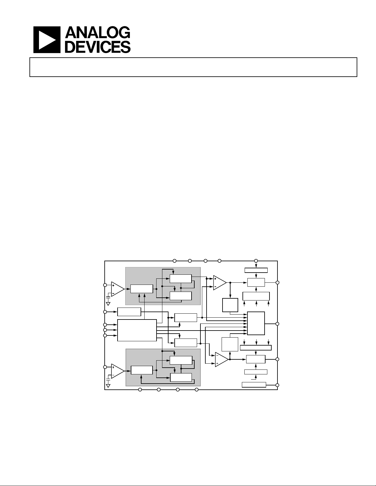
Dual Low Power PLL
V
V
V
V
FEATURES
IDD total: 7.5 mA
Bandwidth RF/IF: 2.4 GHz/1.0 GHz
2.7 V to 3.3 V power supply
Separate V
Programmable dual modulus prescaler
RF and IF: 8/9, 16/17, 32/33, 64/65
Programmable charge pump currents
3-wire serial interface
Analog and digital lock detect
Fastlock mode
Power-down mode
20-lead TSSOP and 20-lead LFCSP packages
APPLICATIONS
Wireless handsets (GSM, PCS, DCS, DSC1800, CDMA,
WCDMA)
Base stations for wireless Radio (GSM, PCS, DCS,
CDMA, WCDMA)
Wireless LANS
Cable TV tuners (CATV)
Communications test equipment
allows extended tuning voltage
P
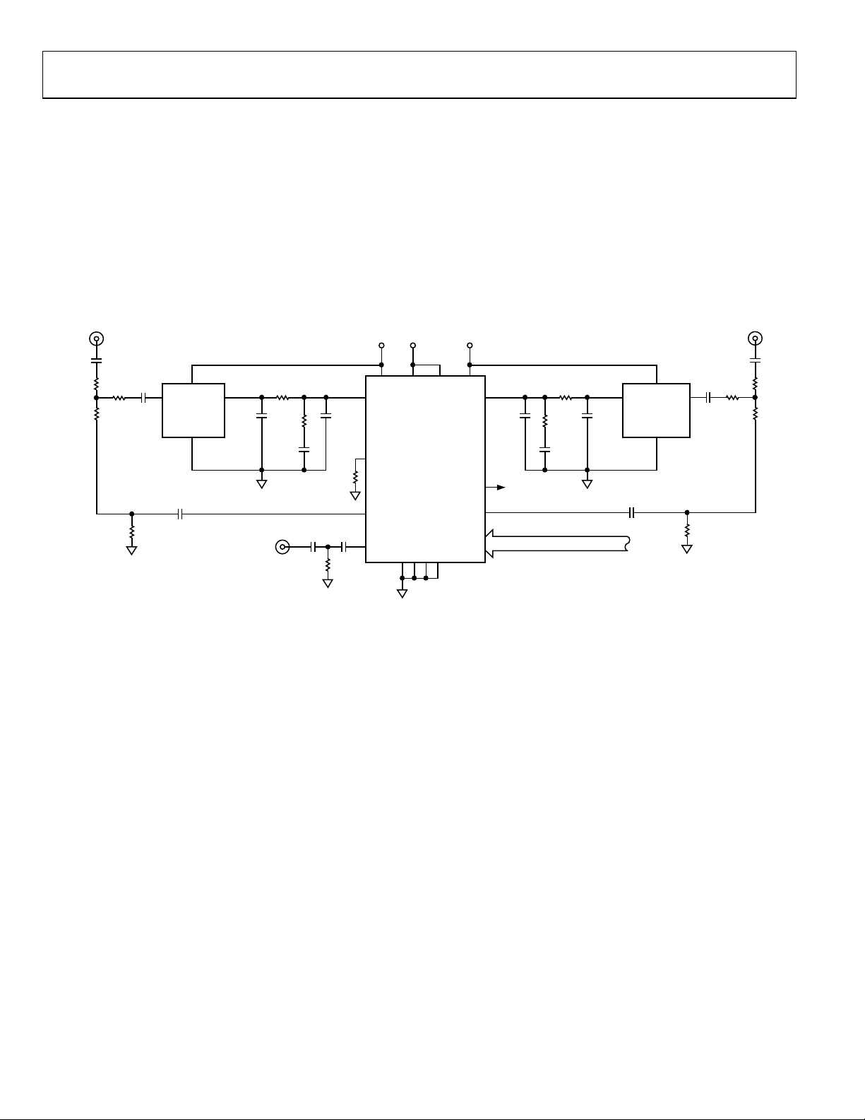
ADF4212L
IF
IN
REF
CLK
DATA
RF
IN
LE
IN
OSCILLATOR
22-BIT
DATA
REGISTER
FUNCTIONAL BLOCK DIAGRAM
IF
PRESCALER
SDOUT
RF
PRESCALER
DGND
AGNDRFDGNDIFAGND
RF
1
DD
12-BIT IF
B-COUNTER
6-BIT IF
A-COUNTER
15-BIT IF
R-COUNTER
15-BIT RF
R-COUNTER
12-BIT RF
B-COUNTER
6-BIT RF
A-COUNTER
Figure 1.
Frequency Synthesizer
ADF4212L
GENERAL DESCRIPTION
The ADF4212L is a dual frequency synthesizer that can be used
to implement local oscillators (LO) in the up-conversion and
down-conversion sections of wireless receivers and transmitters.
It can provide the LO for both the RF and IF sections. It consists
of a low noise digital phase frequency detector (PFD), a precision
charge pump, a programmable reference divider, programmable
A and B counters, and a dual modulus prescaler (P/P + 1). The
A (6-bit) and B (12-bit) counters, in conjunction with the dual
modulus prescaler (P/P + 1), implement an N divider (N = BP +
A). In addition, the 15-bit reference counter (R counter) allows
selectable REF
locked loop (PLL) can be implemented if the synthesizer is used
with external loop filters and voltage controlled oscillators (VCOs).
Control of all the on-chip registers is via a simple 3-wire
interface with 1.8 V compatibility. The devices operate with a
power supply ranging from 2.7 V to 3.3 V and can be powered
down when not in use.
2
1
P
IF PHASE
FREQUENCY
DETECTOR
RF PHASE
FREQUENCY
DETECTOR
2
P
DD
IF
frequencies at the PFD input. A complete phase-
IN
R
SET
REFERENCE
IF
LOCK
DETECT
RF
LOCK
DETECT
CHARGE
PUMP
IF CURRENT
SETTING
IFCP3 IFCP2
OUTPUT
MUX
RFCP3 RFCP2
REFERENCE
CHARGE
PUMP
REFERENCE
R
SET
FLOSWITCH
IFCP1
RFCP1
CP
IF
MUXOUT
CP
RF
FL
O
02774-001
Rev. C
Information furnished by Analog Devices is believed to be accurate and reliable. However, no
responsibility is assumed by Analog Devices for its use, nor for any infringements of patents or other
rights of third parties that may result from its use. Specifications subject to change without notice. No
license is granted by implication or otherwise under any patent or patent rights of Analog Devices.
Trademarks and registered trademarks are the property of their respective owners.
One Technology Way, P.O. Box 9106, Norwood, MA 02062-9106, U.S.A.
Tel: 781.329.4700 www.analog.com
Fax: 781.461.3113 ©2002–2010 Analog Devices, Inc. All rights reserved.

ADF4212L
TABLE OF CONTENTS
Features .............................................................................................. 1
Applications ....................................................................................... 1
General Description ......................................................................... 1
Functional Block Diagram .............................................................. 1
Revision History ............................................................................... 2
Specifications ..................................................................................... 3
Timing Characteristics ................................................................ 5
Absolute Maximum Ratings ............................................................ 6
ESD Caution .................................................................................. 6
Pin Configurations and Function Descriptions ........................... 7
Typical Performance Characteristics ............................................. 9
Circuit Description ......................................................................... 13
Reference Input Section ............................................................. 13
RF/IF Input Stage........................................................................ 13
Prescaler (P/P + 1) ...................................................................... 13
RF/IF A and B Counters ............................................................ 13
Pulse Swallow Function ............................................................. 13
RF/IF R Counter ......................................................................... 13
Phase Frequency Detector (PFD) and Charge Pump ............ 14
MUXOUT and Lock Detect ...................................................... 14
Lock Detect ................................................................................. 14
RF/IF Input Shift Register ......................................................... 14
IF R Counter Latch ..................................................................... 16
IF N Counter Latch .................................................................... 17
RF R Counter Latch ................................................................... 18
RF N Counter Latch ................................................................... 19
Program Modes .............................................................................. 20
IF and RF Power-Down ............................................................. 20
IF Section ..................................................................................... 20
RF Section ................................................................................... 21
Applications Information .............................................................. 22
Local Oscillator for GSM Handset Receiver ............................... 22
Wideband PLL ............................................................................ 23
Interfacing ................................................................................... 24
PCB Design Guidelines for Lead Frame
Chip Scale Package ..................................................................... 24
Outline Dimensions ....................................................................... 25
Ordering Guide .......................................................................... 26
REVISION HISTORY
11/10—Rev. B to Rev C
Changes to V
to V
DD
Changes to Ordering Guide .......................................................... 26
9/08—Rev. A to Rev B
Updated Format .................................................................. Universal
Changes to Figure 1 and General Description Section ............... 1
Changes to Prescaler Output Frequency Parameter and RF
Input Frequency (RF
Changes to Table 3 and Figure 2 ..................................................... 5
Changes to Figure 4 .......................................................................... 7
Changes to Figure 27, RF/IF A and B Counters Section, Pulse
Swallow Function Section, and RF/IF R Counter Section ........ 13
Changes to RF/IF Input Shift Register Section ........................... 14
Changes to Programmable IF Reference (R) Counter Section,
IF Program Modes Section, and IF Power-Down Section ........ 20
1, VP2 to GND Parameter, Table 4 and VP1, VP2
P
1, VDD2 Parameter, Table 4 ................................................... 6
) Parameter ................................................. 3
IN
Changes to Programmable RF Reference (R) Counter Section,
RF Program Modes Section, Programmable RF N Counter
Section, and RF Power-Down Section ......................................... 21
Changes to Figure 32 ...................................................................... 23
Changes to Figure 33 and Figure 34............................................. 24
Added PCB Design Guidelines for Lead Frame Chip Scale
Package Section............................................................................... 24
Updated Outline Dimensions ....................................................... 25
Changes to Ordering Guide .......................................................... 25
3/03—Data Sheet changed from REV. 0 to REV. A
Changes to General Description ..................................................... 1
Changes to Specifications ................................................................. 3
Changes to Table 9 .......................................................................... 18
Changes to Table 11 ....................................................................... 20
Changes to Figure 31 ...................................................................... 23
11/02—Revision 0: Initial Version
Rev. C | Page 2 of 28

ADF4212L
SPECIFICATIONS
VDD1 = VDD2 = 2.7 V to 3.3 V; VP1, VP2 = VDD to 5.5 V; AGNDRF = DGNDRF = AGNDIF = DGNDIF = 0 V; TA = T
otherwise noted; dBm referred to 50 Ω.
Table 1.
Parameter1 B Version B Chips2 Unit Test Conditions/Comments
RF/IF CHARACTERISTICS
RF Input Frequency (RFIN) 0.2/2.4 0.2/2.4 GHz min/max For lower frequencies, ensure that slew rate (SR)
> 140 V/µs
RF Input Sensitivity −10/0 −10/0 dBm min/max VDD = 3 V
IF Input Frequency (IFIN) 100/1000 100/1000 MHz min/max
IF Input Sensitivity −10/0 −10/0 dBm min/max VDD = 3 V
MAXIMUM ALLOWABLE
Prescaler Output Frequency3 188 188 MHz max
REFIN CHARACTERISTICS
See
Figure 26 for input circuit
REFIN Input Frequency 10/150 10/150 MHz min/max
REFIN Input Sensitivity 500 mV/VDD 500 mV/VDD V p-p min/max AC-coupled; when dc-coupled, 0 V to VDD
maximum (CMOS compatible)
REFIN Input Capacitance 10 10 pF max
REFIN Input Current ±100 ±100 A max
PHASE DETECTOR
Phase Detector Frequency4 75 75 MHz max
CHARGE PUMP
ICP Sink/Source
High Value 5 5 mA typ With R
Programmable, see
= 2.7 kΩ
SET
Low Value 625 625 A typ
Absolute Accuracy 2 2 % typ With R
R
Range 1.5/5.6 1.5/5.6 kΩ min/max
SET
= 2.7 kΩ
SET
ICP Three-State Leakage Current 1 1 nA max
Sink and Source Current Matching 6 6 % typ 0.5 V < VCP < VP − 0.5 V
ICP vs. VCP 2 2 % typ 0.5 V < VCP < VP − 0.5 V
ICP vs. Temperature 2 2 % typ VCP = VP/2
LOGIC INPUTS
V
, Input High Voltage 1.4 1.4 V min
INH
V
, Input Low Voltage 0.6 0.6 V max
INL
I
, Input Current ±1 ±1 A max
INH/IINL
CIN, Input Capacitance 10 10 pF max
LOGIC OUTPUTS
VOH, Output High Voltage 1.4 1.4 V min Open-drain 1 kΩ pull-up to 1.8 V
VOL, Output Low Voltage 0.4 0.4 V max IOL = 500 A
POWER SUPPLIES
VDD1 2.7/3.3 2.7/3.3 V min/max
VDD2 VDD1 VDD1 V min/max
VP1, VP2 VDD1/5.5 VDD1/5.5 V min/max
IDD (RF and IF)5 7.5/10 7.5/10 mA typ/max
RF Only 5.0/6 5.0/6 mA typ/max
IF Only 2.5/4 2.5/4 mA typ/max
IP (IP1 + IP2) 0.6 0.6 mA typ
Low Power Sleep Mode 1 1 A typ
1
Operating temperature range is as follows: B version: −40°C to +85°C.
2
The B chip specifications are given as typical values.
3
This is the maximum operating frequency of the CMOS counters. The prescaler value should be chosen to ensure that the RF input is divided down to a frequency less
than this value.
4
Guaranteed by design. Sample tested to ensure compliance.
5
TA = 25°C. RF = 1 GHz; prescaler = 32/33. IF = 500 MHz; prescaler = 16/17.
to T
MIN
Table 10
MAX
, unless
Rev. C | Page 3 of 28

ADF4212L
VDD1 = VDD2 = 2.7 V to 3.3 V; VP1, VP2 = VDD to 5.5 V; AGNDRF = DGNDRF = AGNDIF = DGNDIF = 0 V; TA = T
otherwise noted; dBm referred to 50 V.
Table 2.
Parameter1 B Version B Chips2 Unit Test Conditions/Comments
NOISE CHARACTERISTICS
RF Phase Noise Floor3 −170 −170 dBc/Hz typ 25 kHz PFD frequency
−162 −162 dBc/Hz typ 200 kHz PFD frequency
Phase Noise Performance4 VCO output
IF: 540 MHz Output5 −89 −89 dBc/Hz typ 1 kHz offset and 200 kHz PFD frequency
IF: 900 MHz Output6 −87 −87 dBc/Hz typ 1 kHz offset and 200 kHz PFD frequency
RF: 900 MHz Output6 −89 −89 dBc/Hz typ 1 kHz offset and 200 kHz PFD frequency
RF: 1750 MHz Output7 −84 −84 dBc/Hz typ 1 kHz offset and 200 kHz PFD frequency
RF: 2400 MHz Output8 −87 −87 dBc/Hz typ 1 kHz Offset and 1 MHz PFD frequency
Spurious Signals
IF: 540 MHz Output5 −88/−90 −88/−90 dB typ 200 kHz/400 kHz and 200 kHz PFD frequency
IF: 900 MHz Output6 −90/−94 −90/−94 dB typ 200 kHz/400 kHz and 200 kHz PFD frequency
RF: 900 MHz Output6 −90/−94 −90/−94 dB typ 200 kHz/400 kHz and 200 kHz PFD frequency
RF: 1750 MHz Output7 −80/−82 −80/−82 dB typ 200 kHz/400 kHz and 200 kHz PFD frequency
RF: 2400 MHz Output8 −80/−82 −80/−82 dB typ 200 kHz/400 kHz and 200 kHz PFD frequency
1
Operating temperature range is as follows: B version: −40°C to +85°C.
2
The B Chip specifications are given as typical values.
3
The synthesizer phase noise floor is estimated by measuring the in-band phase noise at the output of the VCO and subtracting 20logN (where N is the N divider value).
See Figure 9.
4
The phase noise is measured with the EVAL-ADF4212EB and the HP8562E spectrum analyzer. The spectrum analyzer provides the REFIN for the synthesizer
(f
= 10 MHz @ 0 dBm).
REFOUT
5
f
REFIN
6
f
REFIN
7
f
REFIN
8
f
REFIN
= 10 MHz; f
= 10 MHz; f
= 10 MHz; f
= 10 MHz; f
= 200 kHz; offset frequency = 1 kHz; fIF = 540 MHz; N = 2700; loop B/W = 20 kHz
PFD
= 200 kHz; offset frequency = 1 kHz; fRF = 900 MHz; N = 4500; loop B/W = 20 kHz
PFD
= 200 kHz; offset frequency = 1 kHz; fRF = 1750 MHz; N = 8750; loop B/W = 20 kHz
PFD
= 1 MHz; offset frequency = 1 kHz; fRF = 2400 MHz; N = 9800; loop B/W = 20 kHz
PFD
MIN
to T
MAX
, unless
Rev. C | Page 4 of 28
ADF4212L
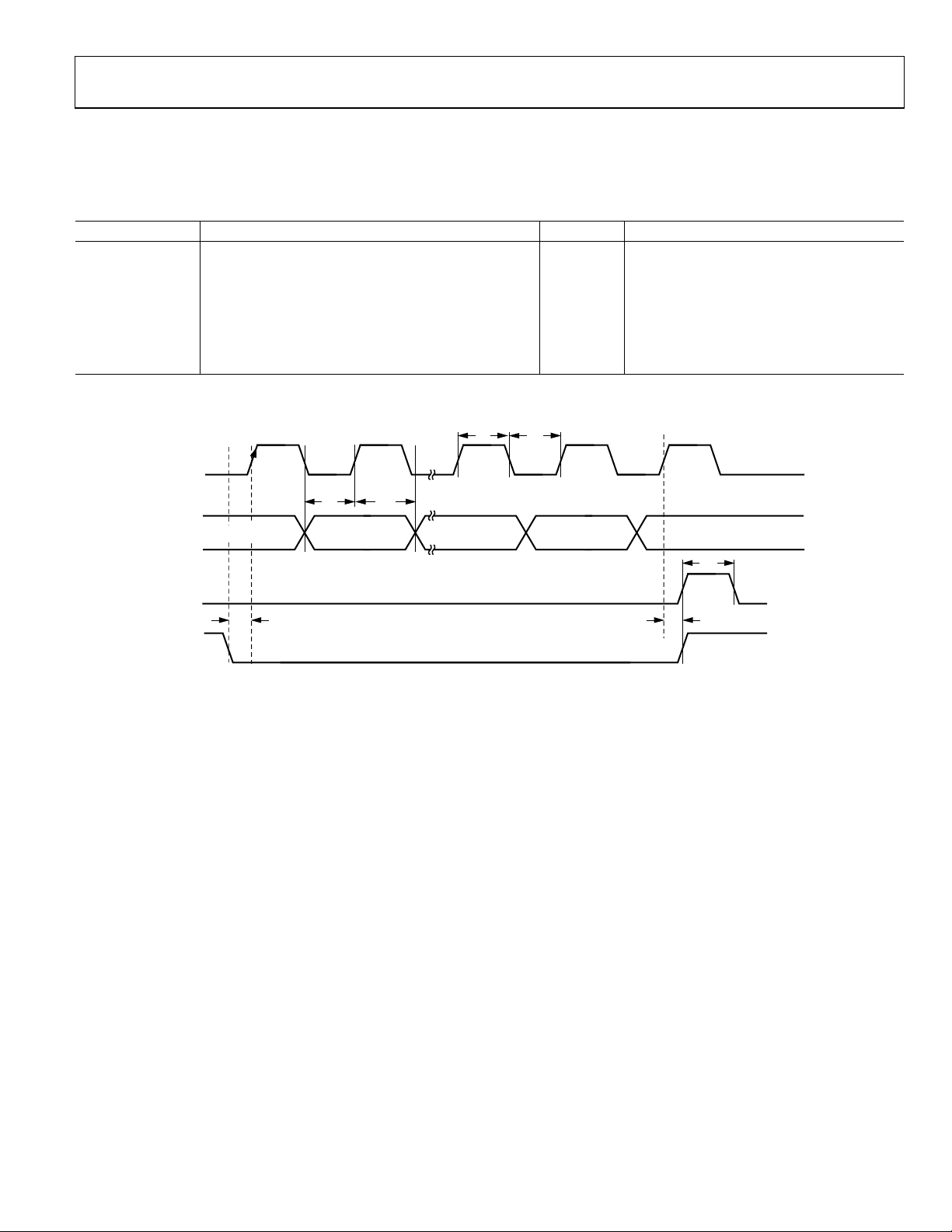
TIMING CHARACTERISTICS
VDD1 = VDD2 = 2.6 V to 3.3 V; VP1, VP2 = VDD to 5.5 V; AGNDRF = DGNDRF = AGNDIF = DGNDIF = 0 V; TA = T
otherwise noted; dBm referred to 50 Ω.
Table 3.
Parameter1 Limit at T
MIN
to T
(B Version) Unit Test Conditions/Comments
MAX
t1 20 ns min LE setup time
t2 10 ns min Data to clock setup time
t3 10 ns min Data to clock hold time
t4 25 ns min Clock high duration
t5 25 ns min Clock low duration
t6 10 ns min Clock to LE setup time
t7 20 ns min LE pulse width
1
Guaranteed by design but not production tested.
CLK
t
4
t
5
MIN
to T
MAX
, unless
DATA
LE
LE
t
2
DB23 (MSB) DB22 DB2
t
1
t
3
DB1
(CONTROL BIT C2)
DB0 (LSB)
(CONTROL BIT C1)
t
7
t
6
02774-002
Figure 2. Timing Diagram
Rev. C | Page 5 of 28
ADF4212L
ABSOLUTE MAXIMUM RATINGS
TA = 25°C, unless otherwise noted.
Table 4.
Parameter
VDD1 to GND −0.3 V to +3.6 V
VDD1 to VDD2 −0.3 V to +0.3 V
VP1, VP2 to GND −0.3 V to +5.8 V
VP1, VP2 to VDD1, VDD2 −0.3 V to +5.8 V
Digital I/O Voltage to GND −0.3 V to DVDD + 0.3 V
Analog I/O Voltage to GND −0.3 V to VDD + 0.3 V
REFIN, RFIN, IFIN to GND −0.3 V to VDD + 0.3 V
Operating Temperature Range
Industrial (B Version) −40°C to +85°C
Storage Temperature Range −65°C to +150°C
Maximum Junction Temperature 150°C
TSSOP θJA Thermal Impedance 150.4°C/W
LFCSP θJA Thermal Impedance
(Paddle Soldered)
LFCSP θJA Thermal Impedance
(Paddle Not Soldered)
Lead Temperature, Soldering
Vapor Phase (60 sec) 215°C
Infrared (15 sec) 220°C
1
This device is a high performance RF integrated circuit with an ESD rating of
<2 kV, and is ESD sensitive. Proper precautions should be taken for handling
and assembly.
3
GND = AGND = DGND = 0 V.
1, 2
Rating
122°C/W
216°C/W
Stresses above those listed under Absolute Maximum Ratings
may cause permanent damage to the device. This is a stress
rating only; functional operation of the device at these or any
other conditions above those indicated in the operational
section of this specification is not implied. Exposure to absolute
maximum rating conditions for extended periods may affect
device reliability.
ESD CAUTION
Rev. C | Page 6 of 28
ADF4212L
2
PIN CONFIGURATIONS AND FUNCTION DESCRIPTIONS
1
1
P
V
20
1CP
RF
VDD1
VP1
CP
DGND
RF
AGND
FL
REF
DGND
MUXOUT
RF
RF
IN
RF
O
IN
IF
1
2
3
ADF4212L
4
(Not to Scale)
5
6
7
8
9
10
TOP VIEW
20
19
18
17
16
15
14
13
12
11
Figure 3. TSSOP Pin Configuration
V
DD
VP2
CP
IF
DGND
IF
IN
AGND
R
SET
LE
DATA
CLK
2
IF
IF
NOTES
1. IT I S RECOMMENDED T HAT THE EXPOSED PAD
BE THERMALLY CONNECTED TO A COPPER PLANE
FOR ENHANCED THERM A L P E RF ORMANCE. THE PAD
2774-003
SHOULD BE GRO UNDED AS WELL.
2DGND
RF
ADF4212L
3RF
IN
RF
O
4AGND
5FL
TOP VIEW
(Not to S cale)
6
IN
REF
Figure 4. LFCSP Pin Configuration
Table 5. Pin Function Descriptions
Pin No.
Mnemonic TSSOP LFCSP Description
CPRF 3 1
RF Charge Pump Output. When enabled, this provides ±I
to the external RF loop filter, which in turn
CP
drives the external RF VCO.
DGNDRF 4 2 Digital Ground Pin for the RF Digital Circuitry.
RFIN 5 3 Input to the RF Prescaler. This small signal input is normally ac-coupled from the RF VCO.
AGNDRF 6 4 Ground Pin for the RF Analog Circuitry.
FLO 7 5 Multiplexed Output of RF/IF Programmable or Reference Dividers, RF/IF Fastlock Mode. CMOS output.
REFIN 8 6
Reference Input. This is a CMOS input with a nominal threshold of V
DD
resistance of 100 kΩ. See Figure 26. This input can be driven from a TTL or CMOS crystal oscillator, or can
be ac-coupled.
DGNDIF 9, 17 7, 15 Digital Ground Pin for the IF Digital, Interface, and Control Circuitry.
MUXOUT 10 8
This multiplexer output allows either the IF/RF lock detect, the scaled RF, the scaled IF, or the scaled
reference frequency to be accessed externally.
CLK 11 9
Serial Clock Input. This serial clock is used to clock in the serial data to the registers. The data is latched
into the 24-bit shift register on the CLK rising edge. This input is a high impedance CMOS input.
DATA 12 10
Serial Data Input. The serial data is loaded MSB first with the two LSBs being the control bits. This input is
a high impedance CMOS input.
LE 13 11
Load Enable, CMOS Input. When LE goes high, the data stored in the shift registers is loaded into one of
the four latches, with the latch selected using the control bits.
R
14 12
SET
Connecting a resistor between this pin and ground sets the maximum RF and IF charge pump output
current. The nominal voltage potential at the R
pin is 0.66 V. The relationship between ICP and R
SET
therefore,
13.5
I
where R
MAXCP
= 2.7 kΩ and ICP
SET
=
R
SET
= 5 mA for both the RF and IF charge pumps.
MAX
AGNDIF 15 13 Ground Pin for the IF Analog Circuitry.
IFIN 16 14 Input to the IF Prescaler. This small signal input is normally ac-coupled from the IF VCO.
CPIF 18 16
Output from the IF Charge Pump. This is normally connected to a loop filter that drives the input to an
external VCO.
VP2 19 17
Power Supply for the IF Charge Pump. This should be greater than or equal to V
2 is 3 V, it can be set to 5.5 V and used to drive a VCO with a tuning range up to 5.5 V.
V
DD
IF
2
P
DD
DD
P
V
C
V
V
17
16
19
18
PIN 1
INDICATOR
8
7
T
IF
D
DGN
MUXOU
15 DGND
IF
14 IF
IN
13 AGND
IF
12 R
SET
11 LE
9
10
CLK
DATA
02774-004
/2 and an equivalent input
2. In systems where
DD
SET
is,
Rev. C | Page 7 of 28

ADF4212L
Pin No.
Mnemonic TSSOP LFCSP Description
VDD2 20 18
VDD1 1 19
VP1 2 20
EP
Exposed
Pad
Power Supply for the IF, Digital, and Interface Section. Decoupling capacitors to the ground plane
should be placed as close as possible to this pin. V
V
2 must have the same potential as VDD1.
DD
2 should have a value of between 2.6 V and 3.3 V.
DD
Power Supply for the RF Section. Decoupling capacitors to the ground plane should be placed as close
as possible to this pin. V
potential as V
2.
DD
Power Supply for the RF Charge Pump. This should be greater than or equal to V
1 is 3 V, it can be set to 5.5 V and used to drive a VCO with a tuning range up to 5.5 V.
V
DD
1 should have a value of between 2.6 V and 3.3 V. VDD1 must have the same
DD
1. In systems where
DD
It is recommended that the exposed pad be thermally connected to a copper plane for enhanced
thermal performance. The pad should be grounded as well.
Rev. C | Page 8 of 28
ADF4212L
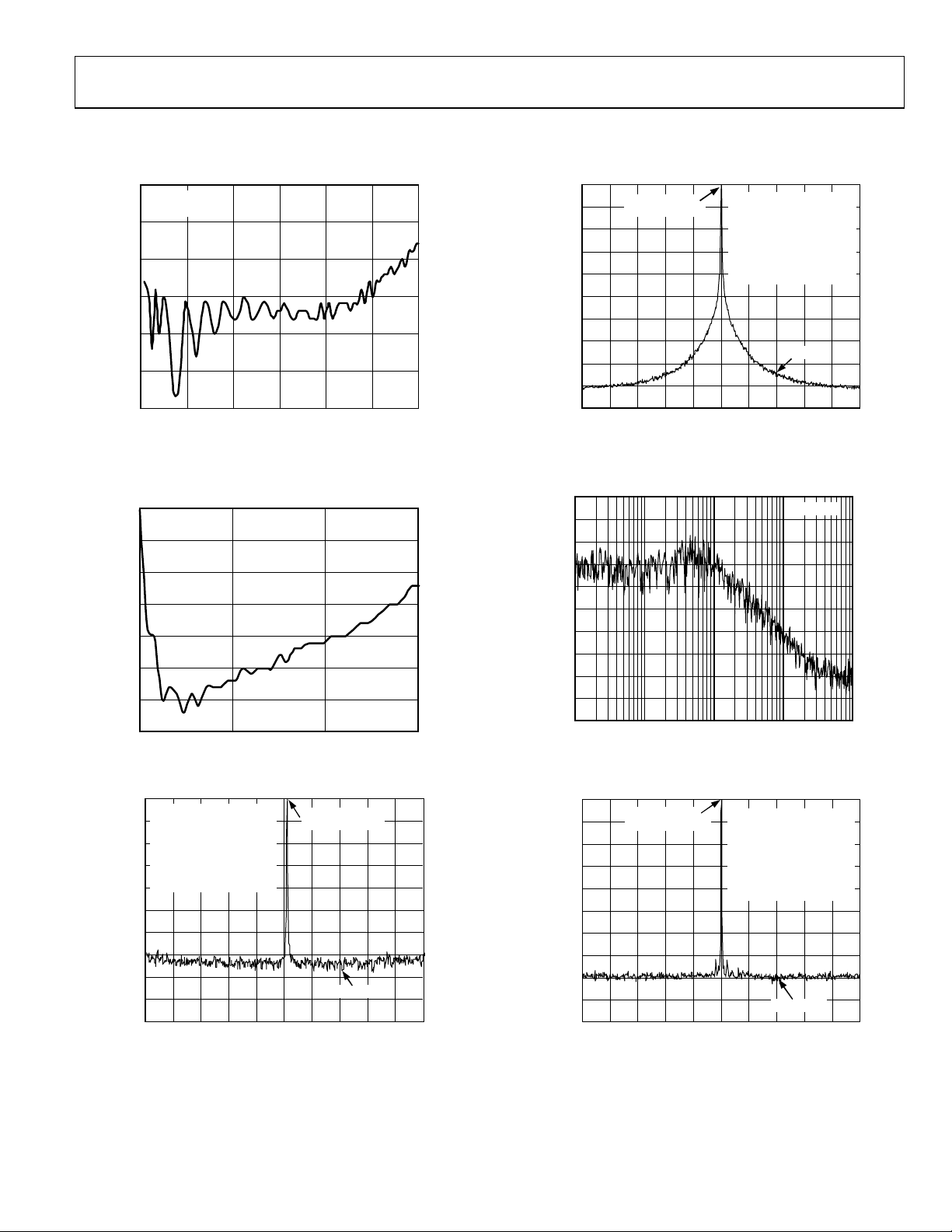
TYPICAL PERFORMANCE CHARACTERISTICS
0
VDD = 3V
V
= 5V
P
–5
–10
–15
–20
AMPLITUDE ( dBm)
–25
–30
0 500 1000 1500 2000
FREQUENCY (MHz)
2500 3000
Figure 5. Input Sensitivity (RF Input)
0
V
= 3V
DD
V
= 5V
P
–5
–10
–15
–20
AMPLITUDE (dBm)
–25
–30
–35
0 500 1000 1500
FREQUENCY (MHz)
Figure 6. Input Sensitivity (IF Input)
0
VDD = 3V, VP = 5V
I
= 5mA
–10
CP
PFD FREQUENCY = 200kHz
LOOP BANDWIDTH = 20kHz
–20
RES. BANDWIDTH = 10Hz
VIDEO BANDWI DTH = 10Hz
–30
SWEEP = 1.9 SECONDS
AVERAGES = 22
–40
–50
–60
–70
OUTPUT POWER (dB)
–80
–90
–100
–2k –1k 1.75G 1k 2k
FREQUENCY (Hz)
REFERENCE
LEVEL = –3. 2d Bm
–84.2dBc/Hz
Figure 7. Phase Noise, RF Side (1750 MHz, 200 kHz, 20 kHz)
0
–10
–20
–30
–40
–50
–60
–70
OUTPUT POWER (dB)
–80
–90
–100
02774-005
REFERENCE
LEVEL = –3.0dBm
–400k –200k 1.75G 200k 400k
FREQUENCY (Hz)
VDD= 3V, VP= 5V
I
= 5mA
CP
PFD FREQUENCY = 200kHz
LOOP BANDW IDTH = 20kHz
RES. BANDWIDT H = 1Hz
VIDEO BANDWIDTH = 1Hz
SWEEP = 2.5 SECONDS
AVERAGES = 20
–85.9dB
02774-008
Figure 8. Reference Spurs, RF Side (1750 MHz, 200 kHz, 20 kHz)
= –50dBc/Hz
10dB/DIV
–50
–60
–70
–80
–90
–100
–110
–120
PHASE NOISE (d Bc/Hz)
–130
–140
–150
100Hz
02774-006
R
L
FREQUENCY OFFSET
FROM 1.75GHz CARRIER
RMS NOISE = 1.38 DEGREES
1.38° RMS
1MHz
02774-009
Figure 9. Integrated Phase Noise (1750 MHz, 200 kHz/20 kHz)
0
–10
–20
–30
–40
–50
–60
–70
OUTPUT PO WER (dB)
–80
–90
–100
02774-007
REFERENCE
LEVEL = –4.3 d Bm
–2k –1k 540M 1k 2k
FREQUENCY (Hz)
V
= 3V, VP= 5V
DD
I
= 5mA
CP
PFD FREQUENCY = 200kHz
LOOP BANDW IDTH = 20kHz
RES. BANDWIDT H = 10Hz
VIDEO BANDWIDTH = 10Hz
SWEEP = 1.9 SECONDS
AVERAGES = 22
–88.8dBc/Hz
02774-010
Figure 10. Phase Noise, IF Side (540 MHz, 200 kHz/20 kHz)
Rev. C | Page 9 of 28

ADF4212L
–
–
OUTPUT PO WER (dB)
–100
0
–10
–20
–30
–40
–50
–60
–70
–80
–90
REFERENCE
LEVEL = –7.0dBm
–400k –200k
FREQUENCY (Hz)
V
= 3V, VP= 5V
DD
I
= 5mA
CP
PFD FREQUENCY = 200kHz
LOOP BANDWIDTH = 20kHz
RES. BANDWIDT H = 1Hz
VIDEO BANDWI DTH = 1Hz
SWEEP = 2.5 SECONDS
AVERAGES = 20
–89.3dBc
540M
200k 400k
Figure 11. Reference Spurs, IF Side (540 MHz, 200 kHz, 20 kHz)
R
10dB/DIV
–50
–60
–70
–80
–90
–100
–110
–120
PHASE NOISE (dBc/Hz)
–130
–140
–150
100Hz 1MHz
= –50dBc/Hz
L
FREQUENCY OF F SE T
FROM 540MHz CARRIER
RMS NOISE =
0.83 DEGREES
0.83° RMS
Figure 12. Integrated Phase Noise (540 MHz, 200 kHz/20 kHz)
02774-011
02774-012
130
–140
–150
–160
PHASE NOISE ( dBc/Hz)
–170
–180
10 10k
PHASE DETECTOR FREQUENCY (kHz )
1k100
V
=3V
DD
=5V
V
P
Figure 14. Phase Noise Referred to CP Output vs. PFD Frequency, IF Side
6
4
2
0
(mA)
CP
I
–2
–4
0
1
2
34–65
VCP (V)
02774-015
Figure 15. RF Charge Pump Output Characteristics
02774-014
130
–140
–150
–160
PHASE NOISE (d Bc/Hz)
–170
–180
10 10k
PHASE DETECTO R FRE Q UENCY (kHz)
VDD=3V
=5V
V
P
1k100
Figure 13. Phase Noise Referred to CP Output vs. PFD Frequency, RF Side
02774-013
Rev. C | Page 10 of 28
6
4
2
(mA)
0
CP
I
–2
–4
–6
0
1
2
34
VCP (V)
Figure 16. IF Charge Pump Output Characteristics
V
DD
V
P
=3V
2 = 5.5V
5
02774-016

ADF4212L
0
–20
–40
–60
–80
FIRST REFERENCE SPUR (dBc)
–100
01234
TUNING VOLTAGE (V)
Figure 17. RF Reference Spurs (200 kHz) vs. V
(1750 MHz, 200 kHz, 20 kHz)
TUNE
5
02774-017
0
–10
–20
–30
–40
–50
–60
–70
PHASE NOISE ( dBc/Hz)
–80
–90
–100
TEMPERATURE ( °C)
100806040200–20–40
Figure 20. IF Phase Noise vs. Temperature (540 MHz, 200 kHz, 20 kHz)
02774-020
0
–20
–40
–60
–80
FIRST REFERENCE SPUR (dBc)
–100
–120
01234
Figure 18. IF Reference Spurs (200 kHz) vs. V
0
–10
–20
–30
–40
–50
–60
–70
PHASE NOISE ( dBc/Hz)
–80
–90
–100
–40 –20 0 20 40 60 80 100
TUNING VOL TAGE ( V )
(1750 MHz, 200 kHz, 20 kHz)
TUNE
TEMPERATURE (°C)
Figure 19. RF Phase Noise vs. Temperature (1750 MHz, 200 kHz, 20 kHz)
0
–10
–20
–30
–40
–50
–60
–70
PHASE NOISE (dBc/Hz)
–80
–90
–100
5
02774-018
02774-019
01234
0
–10
–20
–30
–40
–50
–60
–70
PHASE NOISE ( dBc/Hz)
–80
–90
–100
TUNING VOLTAGE (V)
Figure 21. RF Noise vs. V
TUNING VOL T AG E (V )
Figure 22. IF Noise vs. V
TUNE
TUNE
432105
5
02774-021
02774-022
Rev. C | Page 11 of 28

ADF4212L
0
–20
–40
–60
–80
FIRST REFERENCE SPUR (dBc)
–100
–120
–40 –20 0 20 40 60 80 100
TEMPERATURE (°C)
Figure 23. RF Spurs vs. Temperature
0
–20
–40
–60
–80
FIRST REF E RE NCE S P UR (dBc)
–100
FREQUENCY
(MHz)
50
150
250
350
450
550
650
750
850
950
1050
1150
1250
1350
02774-023
1450
s11.REAL s11.IMAG
0.97692
0.942115
0.961217
0.920667
0.897441
0.888164
0.850012
0.760189
0.767363
0.779511
0.761034
0.624825
0.635364
0.630242
0.634506
–0.021077
–0.110459
–0.085802
–0.185830
–0.245482
–0.282399
–0.305457
–0.358884
–0.541032
–0.585687
–0.482539
–0.530106
–0.590526
–0.592498
–0.655932
FREQUENCY
(MHz)
1550
1650
1750
1850
1950
2050
2150
2250
2350
2450
2550
2650
2750
2850
2950
s11.REAL s11.IMAG
0.561872
0.529742
0.514244
0.405754
0.379354
0.312959
0.322646
0.288881
0.199294
0.206914
0.168344
0.092764
0.036125
0.037007
–0.053842
–0.646879
–0.668172
–0.702192
–0.714541
–0.703593
–0.802878
–0.803970
–0.807055
–0.758619
–0.725029
–0.770837
–0.776619
–0.706197
–0.716939
–0.736527
02774-025
Figure 25. S Parameter Data for the RF Input
–120
TEMPERATURE ( °C)
100806040200–20–40
02774-024
Figure 24. IF Spurs vs. Temperature
Rev. C | Page 12 of 28
ADF4212L
CIRCUIT DESCRIPTION
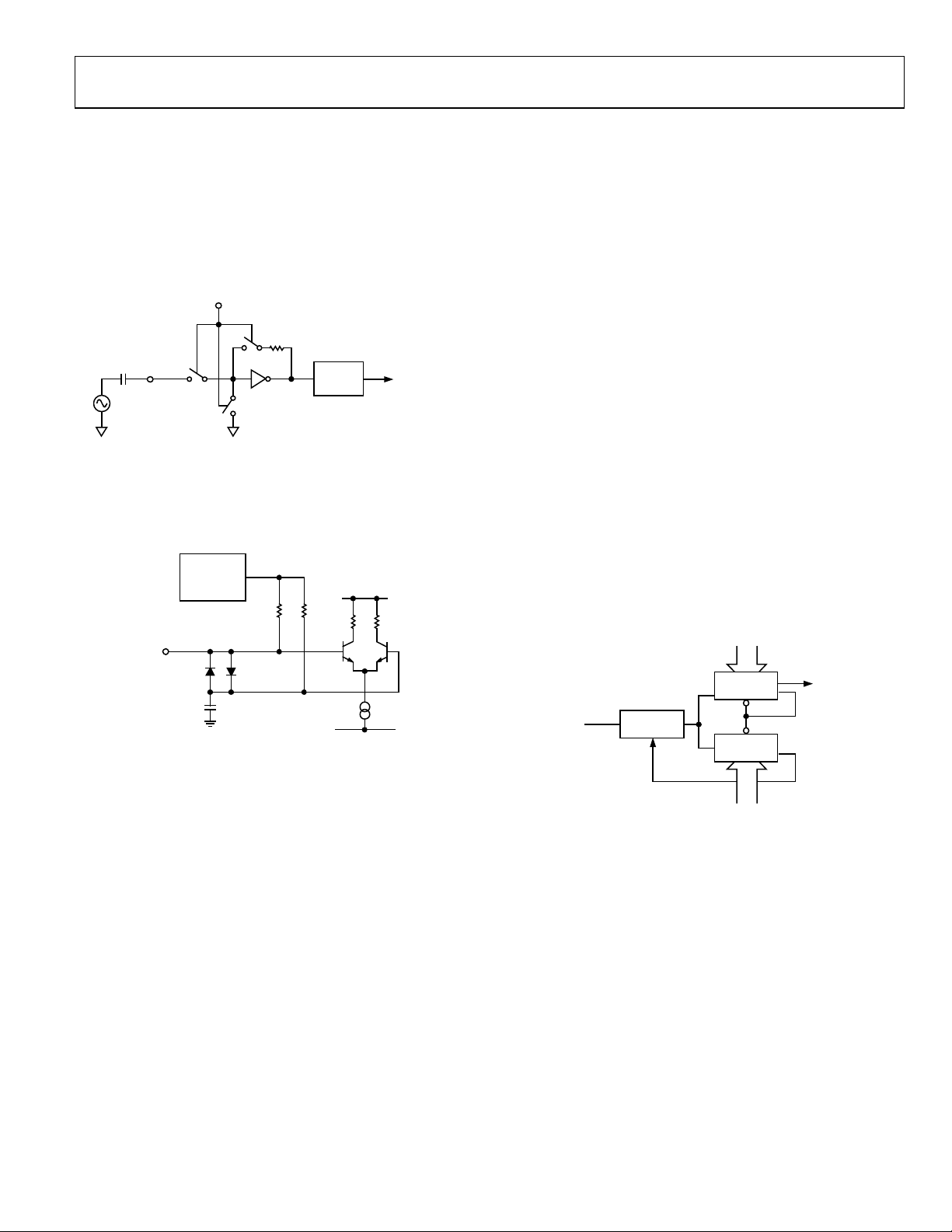
REFERENCE INPUT SECTION
The reference input stage is shown in Figure 26. SW1 and SW2
are normally closed switches. SW3 is normally open. When
power-down is initiated, SW3 is closed and SW1 and SW2 are
opened. This ensures that there is no loading of the REF
IN
pin
on power-down.
POWER-DOWN
CONTROL
100kΩ
NC
NO
SW2
SW3
BUFFER
NC = NO CONNECT
TO R COUNTE R
REF
IN
NC
SW1
Figure 26. Reference Input Stage
RF/IF INPUT STAGE
The RF/IF input stage is shown in Figure 27. It is followed by a
two-stage limiting amplifier to generate the current mode logic
(CML) clock levels needed for the prescaler.
1.6V
2kΩ 2kΩ
AV
AGND
DD
02774-027
RF
IN
BIAS
GENERATOR
100pF
AGND
Figure 27. RF/IF Input Stage
PRESCALER (P/P + 1)
The dual-modulus prescaler (P/P + 1), along with the A and B
counters, enables the large division ratio, N, to be realized (N =
PB + A). The dual modulus prescaler, operating at CML levels,
takes the clock from the RF/IF input stage and divides it down
to a manageable frequency for the A and B CMOS counters in the
RF and IF sections. The prescaler in both sections is programmable. It can be set in software to 8/9, 16/17, 32/33, or 64/65 (see
Tabl e 9 and Tab l e 10). It is based on a synchronous 4/5 core.
02774-026
RF/IF A AND B COUNTERS
The A and B CMOS counters combine with the dual modulus
prescaler to allow a wide ranging division ratio in the PLL
feedback counter. The counters are specified to work when the
prescaler output is 188 MHz or less. Thus, with an RF input
frequency of 2.5 GHz, a prescaler value of 16/17 is valid, but a
value of 8/9 is not valid.
PULSE SWALLOW FUNCTION
The A and B CMOS counters, in conjunction with the dual
modulus prescaler, make it possible to generate output
frequencies that are spaced only by the reference frequency
divided by R. The equation for the VCO frequency is as follows:
f
= [(P × B) + A] × f
VCO
REFIN
/R
where:
f
is the output frequency of external voltage controlled
VCO
oscillator (VCO).
P is the preset modulus of the dual modulus prescaler (8/9,
16/17, and so on).
B is the preset divide ratio of the binary 12-bit counter (3 to 4095).
A is the preset divide ratio of the binary 6-bit swallow counter
(0 to 63).
f
is the external reference oscillator frequency.
REFIN
R is the preset divide ratio of the binary 15-bit programmable
reference counter (1 to 32,767).
FROM RF
INPUT STAGE
MODULUS
CONTROL
N = BP + A
PRESCALER
P/P + 1
Figure 28. RF/IF A and B Counters
12-BIT B
COUNTER
LOAD
LOAD
6-BIT A
COUNTER
TO PFD
02774-028
RF/IF R COUNTER
The 15-bit RF/IF R counter allows the input reference frequency to
be divided down to produce the input clock to the phase frequency
detector (PFD). Division ratios from 1 to 16,383 are allowed.
Rev. C | Page 13 of 28

ADF4212L
PHASE FREQUENCY DETECTOR (PFD) AND CHARGE PUMP
The PFD takes inputs from the R counter and N counter and
produces an output proportional to the phase and frequency
difference between them. Figure 29 is a simplified schematic.
The PFD includes a fixed delay element that sets the width of
the antibacklash pulse. This is typically 3 ns. This pulse ensures
that there is no dead zone in the PFD transfer function and
gives a consistent reference spur level.
UP
U1
CLR1
DELAY
CLR2
DOWN
U2
Figure 29. RF/IF PFD Simplified Schematic
U3
CHARGE
PUMP
CP
02774-029
+IN
–IN
HI
HI
D1 Q1
D2 Q2
MUXOUT AND LOCK DETECT
The output multiplexer on the ADF4212L allows the user to
access various internal points on the chip. The state of MUXOUT
is controlled by P3, P4, P11, and P12 (see Tab le 8 and Tabl e 10 ).
Figure 30 shows the MUXOUT section in block diagram form.
LOCK DETECT
MUXOUT can be programmed for two types of lock detect: digital
lock detect and analog lock detect. Digital lock detect is active
high. It is set high when the phase error on three consecutive phase
detector cycles is less than 15 ns. It stays set high until a phase
error of greater than 25 ns is detected on any subsequent PD cycle.
The N-channel open-drain analog lock detect should be operated
with an external pull-up resistor of 10 kΩ nominal. When lock
has been detected, it is high with narrow, low-going pulses.
DV
DD
IF ANALOG LOCK DETECT
IF R COUNTER OUTP UT
IF N COUNTER OUTP UT
IF/RF ANA LOG LOCK DETECT
RF R COUNTER OUTPUT
RF N COUNTER OUTPUT
RF ANALOG LOCK DETECT
Figure 30. MUXOUT Schematic
MUX CONTROL
MUXOUT
DGND
RF/IF INPUT SHIFT REGISTER
The ADF4212L digital section includes a 24-bit input shift
register, a 15-bit IF R counter, and an 18-bit IF N counter
(comprising a 6-bit IF A counter and a 12-bit IF B counter).
Also present is a 15-bit RF R counter and an 18-bit RF N
counter (comprising a 6-bit RF A counter and a 12-bit RF B
counter). Data is clocked into the 24-bit shift register on each
rising edge of CLK. The data is clocked in MSB first. Data is
transferred from the shift register to one of four latches on the
rising edge of LE. The destination latch is determined by the
state of the two control bits (C2, C1) in the shift register. These
are the two LSBs, DB1 and DB0, as shown in the timing diagram
of Figure 2. The truth table for these bits is shown in Tab le 6 .
Tabl e 7 shows a summary of how the latches are programmed.
Table 6. C2, C1 Truth Table
Control Bits
C2 C1 Data Latch
0 0 IF R counter
0 1 IF N counter (A and B)
1 0 RF R counter
1 1 RF N counter (A and B)
2774-030
Rev. C | Page 14 of 28
ADF4212L
Table 7. Latch Summary
IF R COUNTER LATCH
IF CP CURRENT
SETTING
DB23
DB22
DB21
IFCP2
IFCP1
IFCP0
IF
SETTING
DB22
RFCP1
PRESCALER
POWER-DOWN
DB21
RFCP0
GAIN
IF CP
DB23P8DB22P7DB21
RF CP CURRENT
DB23
RFCP2
O
IF F
CP
IF PD
PRECISION
LOCK DETECT
POLARITY
THREE-STATE
P1
R15
15-BIT REFERENCE COUNTER
CONTROL
BITS
DB0DB1DB2DB3DB4DB5DB6DB7DB8DB9DB10DB11DB12DB13DB14DB15DB16DB17DB18DB19DB20
C1 (0)C2 (0)R1R2R3R4R5R6R7R8R9R10R11R12R13R14P2P3P4
IF N COUNTER LATCH
IF
P6
B10
B9
12-BIT B COUNT E R
6-BIT A COUNT E R
CONTROL
BITS
DB0DB1DB2DB3DB4DB5DB6DB7DB8DB9DB10DB11DB12DB13DB14DB15DB16DB17DB18DB19DB20
C1 (1)C2 (0)A1A2A3A4A5A6B1B2B3B4B5B6B7B8B11B12P5
RF R COUNTER LATCH
O
RF F
RF LOCK
CP
DETECT
RF PD
POLARITY
THREE-STATE
P9
R15
15-BIT RF REFERENCE COUNTE R
CONTROL
BITS
DB0DB1DB2DB3DB4DB5DB6DB7DB8DB9DB10DB11DB12DB13DB14DB15DB16DB17DB18DB19DB20
C1 (0)C2 (1)R1R2R3R4R5R6R7R8R9R10R11R12R13R14P10P11P12
RF N COUNTER LATCH
RF C
DB23
P17
PRESCALER
POWER-DOWN
DB21
P15
RF
B10
RF
GAIN
DB22
P16
B9
12-BIT B COUNT E R
6-BIT A COUNT E R
CONTROL
BITS
DB0DB1DB2DB3DB4DB5DB6DB7DB8DB9DB10DB11DB12DB13DB14DB15DB16DB17DB18DB19DB20
C1 (1)C2 (1)A1A2A3A4A5A6B1B2B3B4B5B6B7B8B11B12P14
02774-031
Rev. C | Page 15 of 28

ADF4212L
IF R COUNTER LATCH
Table 8. IF R Counter Latch Map
IF CP CURRENT
SETTING
DB23
DB22
IFCP2
IFCP1
DB21
IFCP0
O
IF F
CP
IF PD
PRECISION
LOCK DETECT
POLARITY
THREE-STATE
P1
R15
P1 IF PD POLARITY
0
NEGATIVE
1
POSITIVE
CHARGE PUMP
P2
OUTPUT
NORMAL
0
1
THREE-STATE
15-BIT IF REFERENCE CO UNT ER
R15 R14 R13 .......... R3 R2 R1 DIVIDE RATIO
1
0
0
0
0
0
0
0
0
.
.
.
.
.
.
1
1
1
1
1
1
1
1
..........
0
..........
0
..........
0
..........
.
..........
.
..........
.
..........
1
..........
1
..........
1
..........
1
..........
0
0
0
0
0
1
.
.
.
1
1
1
1
0
1
1
1
0
0
.
.
.
.
.
.
0
0
1
0
0
1
1
1
CONTROL
BITS
1
2
3
4
.
.
.
32764
32765
32766
32767
DB0DB1DB2DB3DB4DB5DB6DB7DB8DB9DB10DB11DB12DB13DB14DB15DB16DB17DB18DB19DB20
C1 (0)C2 (0)R1R2R3R4R5R6R7R8R9R10R11R12R13R14P2P3P4
P12 P11 P4 P3
0
0
0
0
0
0
0
0
1
1
1
1
1
1
1
1
IFCP2 IFCP1 IFCP0
0
0
0
0
0
0
1
1
1
1
1
0
0
1
1
1
0
0
1
0
0
1
1
1
0
0
0
0
0
1
0
1
1
0
1
0
1
1
1
1
0
0
0
0
0
1
0
1
1
0
1
0
1
1
1
1
I
(mA)
CP
1.5kΩ 2.7kΩ 5.6kΩ
1.1250
2.2500
3.3750
4.5000
5.6250
6.7500
7.7875
9.0000
0.625
1.250
1.875
2.500
3.125
3.750
4.375
5.000
0.301
0.602
0.904
1.205
1.506
1.808
2.109
2.411
MUXOUTFROM RF R LATCH
0
LOGIC LOW STATE
1
IF ANALOG LOCK DETECT
0
IF REFERENCE DIVIDER OUT P UT
1
IF N DIVI DER OUTPUT
0
RF ANALOG L OCK DETECT
1
RF/IF ANAL OG LOCK DE T ECT
0
IF DIGITAL LOCK DETECT
1
LOGIC HIGH STATE
0
RF REFERENCE DI V IDER OUTPUT
1
RF N DIVIDER O UTPUT
0
THREE-STAT E OUTPUT
1
IF COUNTE R RES E T
0
RF DIGITAL LOCK DET ECT
1
RF/IF DIGITAL LOCK DET ECT
0
RF COUNTER RESE T
1
IF AND RF COUNT ER RESET
02774-032
Rev. C | Page 16 of 28

ADF4212L
IF N COUNTER LATCH
Table 9. IF N Counter Latch Map
IF
IF CP
GAIN
DB23P8DB22P7DB21
P8 IF CP GAIN
01DISABLED
PRESCALER
POWER-DOWN
P6
P7 IF POWER-DO W N
01DISABLED
ENABLED
ENABLED
IF
P5
P6 PRESCALER VALUE
0
0
8/9
1
0
16/17
0
1
32/33
1
1
64/65
B12 B11 B10 B3 B2 B1 B COUNTER DIVIDE RATIO
0
0
0
0
.
.
.
1
1
1
1
0
0
.
.
.
.
.
.
1
1
1
1
1
1
1
1
B9
..........
..........
..........
..........
..........
..........
..........
..........
..........
12-BIT B COUNT E R
1
0
0
1
.
.
.
.
.
.
0
1
0
1
1
1
1
1
A6 A5 .......... A2 A1
0
0
0
0
.
.
.
1
1
1
1
1
0
.
.
.
0
1
0
1
3
4
.
.
.
4092
4093
4094
4095
0
0
0
0
.
.
.
1
1
1
1
6-BIT A COUNT E R
..........
..........
..........
..........
..........
..........
..........
..........
..........
..........
..........
0
0
1
0
.
.
.
0
0
1
1
0
1
0
1
.
.
.
0
1
0
1
CONTROL
BITS
DB0DB1DB2DB3DB4DB5DB6DB7DB8DB9DB10DB11DB12DB13DB14DB15DB16DB17DB18DB19DB20
C1 (1)C2 (0)A1A2A3A4A5A6B1B2B3B4B5B6B7B8B11B12P5 B10
A COUNTER
DIVIDE RATI O
0
1
2
3
.
.
.
60
61
62
63
Rev. C | Page 17 of 28
N = BP + A, P IS PRESCALER VALUE SET IN THE FUNCTION LATCH.
B MUST BE GREAT E R THAN OR EQUAL TO A.
FOR CONTIGUOUS VALUES OF N, N
IS (p2 – P).
MIN
02774-033

ADF4212L
RF R COUNTER LATCH
Table 10. RF R Counter Latch Map
RF CP CURRENT
SETTING
DB23
DB22
RFCP2
RFCP1
DB21
RFCP0
O
RF LOCK
CP
DETECT
RF PD
POLARITY
THREE-STATE
P9
R15
P9 RF PD POLARITY
01NEGATIVE
POSITIVE
CHARGE PUMP
P10
OUTPUT
NORMAL
0
1
THREE-STATE
RF F
15-BIT RF REFERENCE COUNTE R
R15 R14 R13 .......... R3 R2 R1 DIVIDE RATIO
1
0
0
0
0
0
0
0
0
.
.
.
.
.
.
1
1
1
1
1
1
1
1
..........
0
..........
0
..........
0
..........
.
..........
.
..........
.
..........
1
..........
1
..........
1
..........
1
..........
0
0
0
0
0
1
.
.
.
1
1
1
1
0
1
1
1
0
0
.
.
.
.
.
.
0
0
1
0
0
1
1
1
CONTROL
1
2
3
4
.
.
.
32764
32765
32766
32767
BITS
DB0DB1DB2DB3DB4DB5DB6DB7DB8DB9DB10DB11DB12DB13DB14DB15DB16DB17DB18DB19DB20
C1 (0)C2 (0)R1R2R3R4R5R6R7R8R9R10R11R12R13R14P10P11P12
P12 P11 P4 P3 MUXOUT
0
0
0
0
0
0
0
0
1
1
1
1
1
1
1
1
RFCP2 RFCP1 RFCP0
0
0
0
0
0
0
1
1
1
1
1
0
0
1
1
1
0
0
1
0
0
1
1
1
FROM IF R LATCH
0
0
0
0
0
1
0
1
1
0
1
0
1
1
1
1
0
0
0
0
0
1
0
1
1
0
1
0
1
1
1
1
I
(mA)
CP
1.5kΩ 2.7kΩ 5.6kΩ
1.1250
2.2500
3.3750
4.5000
5.6250
6.7500
7.7875
9.0000
0.625
1.250
1.875
2.500
3.125
3.750
4.375
5.000
0.301
0.602
0.904
1.205
1.506
1.808
2.109
2.411
0
LOGIC LOW STATE
1
IF ANALOG LOCK DETECT
0
IF REFERENCE DIVIDER OUT P UT
1
IF N DIVI DER OUTPUT
0
RF ANALOG L OCK DETECT
1
RF/IF ANAL OG LOCK DE T ECT
0
IF DIGITAL LOCK DETECT
1
LOGIC HIGH STATE
0
RF REFERENCE DI V IDER OUTPUT
1
RF N DIVIDER O UTPUT
0
THREE-STAT E OUTPUT
1
IF COUNTE R RES E T
0
RF DIGITAL LOCK DET ECT
1
RF/IF DIGITAL LOCK DET ECT
0
RF COUNTER RESE T
1
IF AND RF COUNT ER RESET
02774-034
Rev. C | Page 18 of 28
ADF4212L
RF N COUNTER LATCH
Table 11. RF N Counter Latch Map
RF
RF CP
GAIN
DB23
DB22
P17
P16
P16 RF POWER-DOWN
01DISABLED
P17 RF CP GAIN
01DISABLED
ENABLED
RF
PRESCALER
POWER-DOWN
DB21
P15
P14
P15 PRESCALER VALUE
0
0
1
0
0
1
1
1
ENABLED
B12 B11 B10 B3 B2 B1 B COUNTER DIVIDE RATIO
0
0
.
.
.
1
1
1
1
8/9
16/17
32/33
64/65
0
1
0
1
.
.
.
0
1
0
1
CONTROL
BITS
DB0DB1DB2DB3DB4DB5DB6DB7DB8DB9DB10DB11DB12DB13DB14DB15DB16DB17DB18DB19DB20
C1 (1)C2 (1)A1A2A3A4A5A6B1B2B3B4B5B6B7B8B11B12P14 B10
DIVIDE RATI O
0
1
2
3
.
.
.
60
61
62
63
12-BIT B COUNT E R
B9
A6 A5 .......... A2 A1 A COUNTER
0
0
0
0
.
.
.
1
1
1
1
0
0
.
.
.
1
1
1
1
..........
0
..........
.
..........
.
..........
.
..........
1
..........
1
..........
1
..........
1
..........
0
0
1
.
.
.
1
1
1
1
0
0
.
.
.
.
.
.
0
0
1
0
0
1
1
1
1
1
3
4
.
.
.
4092
4093
4094
4095
0
0
0
0
.
.
.
1
1
1
1
6-BIT A COUNT E R
..........
..........
..........
..........
..........
..........
..........
..........
..........
..........
..........
0
0
1
0
.
.
.
0
0
1
1
N = BP + A, P IS P RE SCALER VALUE SET IN THE FUNCT ION LATCH
B MUST BE GREAT E R THAN OR EQUAL TO A
FOR CONTIGUOUS VALUE S OF N, N
IS (P2 – P)
MIN
02774-035
Rev. C | Page 19 of 28

ADF4212L
PROGRAM MODES
Tabl e 8 and Tab l e 10 show how to set up the program modes in
the ADF4212L. The following should be noted:
• IF and RF analog lock detect indicate when the PLL is in
lock. When the loop is locked and either IF or RF analog
lock detect is selected, the MUXOUT pin shows a logic
high with narrow, low-going pulses. When the IF/RF
analog lock detect is chosen, the locked condition is
indicated only when both IF and RF loops are locked.
• The IF counter reset mode resets the R, A, and B counters
in the IF section and puts the IF charge pump into threestate mode. The RF counter reset mode resets the R, A, and
B counters in the RF section and puts the RF charge pump
into three-state. The IF and RF counter reset mode does
both of the above. Upon removal of the reset bits, the A
and B counters resume counting in close alignment with
the R counter. (Maximum error is one prescaler output cycle.)
• The fastlock mode uses MUXOUT to switch a second loop
filter damping resistor to ground during fastlock operation.
Activation of fastlock occurs whenever RF CP gain in the
RF reference counter is set to 1.
IF AND RF POWER-DOWN
It is possible to program the ADF4210 family for either synchronous or asynchronous power-down on either the IF or RF side.
Synchronous IF Power-Down
Programming a 1 to P7 of the ADF4212L initiates a powerdown. If P2 of the ADF4212L has been set to 0 (normal
operation), a synchronous power-down is conducted. The
device automatically puts the charge pump into three-state
mode and completes the power-down.
Asynchronous IF Power-Down
If P2 of the ADF4212L has been set to 1 (the IF charge pump in
three-state mode) and P7 is subsequently set to 1, an asynchronous
power-down is conducted. The device goes into power-down on
the rising edge of LE, which latches the 1 to the IF power-down
bit (P7).
Synchronous RF Power-Down
Programming a 1 to P16 of the ADF4212L initiates a powerdown. If P10 of the ADF4212L has been set to 0 (normal
operation), a synchronous power-down is conducted. The
device automatically puts the charge pump into three-state
mode and then completes the power-down.
Asynchronous RF Power-Down
If P10 of the ADF4212L has been set to 1 (the RF charge pump in
three-state mode) and P16 is subsequently set to 1, an asynchronous power-down is conducted. The device goes into power-down
on the rising edge of LE, which latches the 1 to the RF power-down
bit (P16).
Activation of either synchronous or asynchronous power-down
forces the IF/RF loop’s R and A/B dividers to their load state
conditions, and the IF/RF input section is debiased to a high
impedance state.
The REF
RF power-downs are set.
The input register and latches remain active and are capable of
loading and latching data during all power-down modes.
The IF/RF section of the device returns to normal powered-up
operation immediately upon LE latching a 0 to the appropriate
power-down bit.
oscillator circuit is disabled only if both the IF and
IN
IF SECTION
Programmable IF Reference (R) Counter
If Control Bits[C2:C1] = 00, the data is transferred from the
input shift register to the 15-bit IF R counter. Ta ble 8 shows the
input shift register data format for the IF R counter and the
divide ratios that are possible.
IF Phase Detector Polarity
P1 sets the IF phase detector polarity. When the IF VCO
characteristics are positive, P1 should be set to 1. When
the IF VCO characteristics are negative, it should be set to 0.
See Tab le 8 .
IF Charge Pump Three-State
P2 puts the IF charge pump into three-state mode when
programmed to a 1. It should be set to 0 for normal operation.
See Tab le 8 .
IF Program Modes
Tabl e 8 shows how to set up the program modes in the
ADF4212L.
IF Charge Pump Currents
IFCP2, IFCP1, and IFCP0 program the current setting for the
IF charge pump. See Tabl e 8.
Programmable IF N Counter
If Control Bits[C2:C1] = 01, the data in the input register is
used to program the IF N (A + B) counter. The N counter
consists of a 6-bit swallow counter (A counter) and 12-bit
programmable counter (B counter). Ta ble 9 shows the input
register data format for programming the IF A and B counters
and the divide ratios possible.
IF Prescaler Value
P5 and P6 in the IF N counter latch set the IF prescaler values.
See Tab le 9 .
Rev. C | Page 20 of 28

ADF4212L
IF Power-Down
Tabl e 9 shows the power-down bits in the ADF4212L.
IF Fastlock
The IF CP gain bit (P8) of the IF N counter latch register in the
ADF4212L is the fastlock enable bit. Only when P8 is set to 1 is
IF fastlock enabled. When fastlock is enabled, the IF CP current
is set to the maximum value. Also, an extra loop filter damping
resistor to ground is switched in using the FL
compensating for the change in loop characteristics while in
fastlock. Because the IF CP gain bit is contained in the IF N
counter, only one write is needed to both program a new output
frequency and initiate fastlock. To come out of fastlock, the IF
CP gain bit on the IF N counter latch register must be set to 0
(see Tabl e 9).
pin, thus
O
RF SECTION
Programmable RF Reference (R) Counter
If Control Bits[C2: C1] = 10, the data is transferred from the
input shift register to the 15-bit RF R counter. Table 1 0 shows
the input shift register data format for the RF R counter and the
divide ratios possible.
RF Phase Detector Polarity
P9 sets the IF phase detector polarity. When the RF VCO
characteristics are positive, P9 should be set to 1. When they are
negative, it should be set to 0 (see Ta b le 1 0).
RF Charge Pump Three-State
P10 puts the RF charge pump into three-state mode when
programmed to a 1. It should be set to 0 for normal operation
(see Tabl e 10 ).
RF Program Modes
Tabl e 10 shows how to set up the program modes in the
ADF4212L.
RF Charge Pump Currents
RFCP2, RFCP1, and RFCP0 program the current setting for the
RF charge pump. See Tab l e 1 0 .
Programmable RF N Counter
If Control Bits[C2:C1] = 11, the data in the input register is
used to program the RF N (A + B) counter. The N counter
consists of a 6-bit swallow counter (A counter) and a 12-bit
programmable counter (B counter). Ta ble 1 1 shows the input
register data format for programming the RF N counter and the
divide ratios that are possible.
RF Prescaler Value
P14 and P15 in the RF N counter latch set the RF prescaler
values. See Tabl e 11.
RF Power-Down
Tabl e 11 shows the power-down bits in the ADF4212L.
RF Fastlock
The RF CP gain bit (P17) of the RF N counter latch register in
the ADF4212L is the fastlock enable bit. Only when P17 is set to
1 is IF fastlock enabled. When fastlock is enabled, the RF CP
current is set to the maximum value. Also, an extra loop filter
damping resistor to ground is switched in using the FL
thus compensating for the change in loop characteristics while
in fastlock. Because the RF CP gain bit is contained in the RF N
counter, only one write is needed to both program a new output
frequency and initiate fastlock. To come out of fastlock, the RF
CP gain bit on the RF N counter latch register must be set to 0.
See Tab l e 11.
pin,
O
Rev. C | Page 21 of 28
ADF4212L
APPLICATIONS INFORMATION
LOCAL OSCILLATOR FOR GSM HANDSET RECEIVER
Figure 31 shows the ADF4212L being used with a VCO to produce the required LOs for a GSM base station transmitter or
receiver. The reference input signal is applied to the circuit at
FREF
and, in this case, is terminated in 50 Ω. Typical GSM
IN
systems have a 13 MHz TCXO driving the reference input
without any 50 Ω termination. To have a channel spacing of
200 kHz (the GSM standard), the reference input must be
divided by 65, using the on-chip reference.
The RF output frequency range is 880 MHz to 915 MHz. The
loop filter is designed to give a 20 kHz loop bandwidth. The
filter is set up for a 5 mA charge pump current, and the VCO
sensitivity is 12 MHz/V. The IF output is fixed at 540 MHz. The
filter is again designed to have a bandwidth of 20 kHz, and the
system is programmed to give channel steps of 200 kHz.
100pF
18Ω
18Ω
100pF
18Ω
RF
OUT
18Ω
18Ω
IF
OUT
18Ω
100pF
V
CC
VCO190-540T
3.3kΩ
1.7kΩ
V
V
DD
P
VP2V
V
DD2VDD
CP
IF
620pF1.3nF
V
P
1
1
CP
P
RF
1nF
3.3kΩ
5.6kΩ
620pF
V
VCO190-902U
100pF
CC
ADF4212L
8.2nF
100pF
51Ω
02774-036
51V
13nF
2.7kΩ
100pF
FREF
IN
51Ω
DECOUPLING CAPACITORS (2 2µ F/10pF) ON VDD, VP OF THE ADF 4 212L AND ON VCC OF THE VCOs
HAVE BEEN OMITTED FROM THE DIAGRAM T O AID CLARITY.
R
SET
MUXOUT
DGND
RF
IF
IF
DATA
AGND
IF
IN
RF
100pF100pF
REF
RF
IN
DGND
AGND
LOCK
DETECT
IN
CLK
SPI-COMPATIBLE SERIAL BUS
LE
Figure 31. GSM Handset Receiver Local Oscillator Using the ADF4212L
Rev. C | Page 22 of 28

ADF4212L
S
WIDEBAND PLL
Many of the wireless applications for synthesizers and VCOs in
PLLs are narrow band in nature. These applications include the
various wireless standards such as GSM, DSC1800, CDMA, or
WCDMA. In each of these cases, the total tuning range for the
LO is less than 100 MHz. However, there are also wideband
applications where the LO can have up to an octave tuning
range. For example, cable television tuners have a total range
of about 400 MHz. Figure 32 shows an application where the
ADF4212L is used to control and program the Micronetics
M3500-1324. The loop filter was designed for an RF output of
2100 MHz, a loop bandwidth of 40 kHz, a PFD frequency of 1
MHz, I
factor of 4), VCO K
at an output of 2100 MHz), and a phase margin of 45 degrees.
of 10 mA (2.5 mA synthesizer ICP multiplied by the gain
CP
of 80 MHz/V (sensitivity of the M3500-1324
D
FREF
V
P
VDD1
1000pF1000pF
IN
51Ω
REF
V
DD
V
2
DD
IN
VP2VP1
CP
RF
R
SET
ADF4212L
CLK
PI-COMPATIBLE SERIAL BUS
DATA
LE
DGND
MUXOUT
RF
RF
RF
IF
AGND
DGND
IN
IF
AGND
DECOUPLING CAPACITORS O N V
AND ON V
THE IF SE CTION OF THE CIRCUIT HAS AL SO BEEN OMI TTED TO SIMPLIFY THE SCHEMAT IC.
Figure 32. Wideband PLL Circuit
2.7kΩ
LOCK
DETECT
100pF
OF THE M 3500- 132 4 HAVE BEEN OMI T TED FROM THE DIAGRAM TO AID CLARITY.
CC
3.9nF 27nF
In narrow-band applications, there is generally a small variation
in output frequency (generally less than 10%) and a small variation
in VCO sensitivity over the range (typically <10%). However, in
wideband applications, both of these parameters have a much
greater variation, which changes the loop bandwidth. This, in turn,
can affect stability and lock time. By changing the programmable I
, it is possible to obtain compensation for these varying loop
CP
conditions and to ensure that the loop is always operating close
to optimal conditions.
RF
100pF
18Ω
51Ω
20V
1kΩ
20kΩ
130pF
470Ω
AND VPx OF THE ADF4212L, O N + VS OF THE AD820,
DDx
3kΩ
AD820
12V
V
V_TUNE OUT
M3500-1324
GND
CC
100pF
OUT
18Ω
18Ω
02774-037
Rev. C | Page 23 of 28

ADF4212L
INTERFACING
The ADF4212L has a simple SPI-compatible interface for
writing to the device. CLK, DATA, and LE control the data
transfer. When latch enable (LE) goes high, the 22 bits that have
been clocked into the input register on each rising edge of CLK are
transferred to the appropriate latch. See Figure 2 for the timing
diagram and Tab le 6 for the latch truth table.
The maximum allowable serial clock rate is 20 MHz. This means
that the maximum update rate possible for the device is 909 kHz or
one update every 1.1 μs, which is more than adequate for systems
that have typical lock times in hundreds of microseconds.
ADuC812 Interface
Figure 33 shows the interface between the ADF4212L and the
ADuC812 MicroConverter®. Because the ADuC812 is based on
an 8051 core, this interface can be used with any 8051-based
microcontroller. The microconverter is set up for SPI (serial
port interface) master mode with CPHA = 0. To initiate the
operation, the I/O port driving LE is brought low. Each latch of
the ADF4212L needs a 24-bit word. This is accomplished by
writing three 8-bit bytes from the microconverter to the device.
When the third byte has been written, the LE input should be
brought high to complete the transfer.
When first applying power to the ADF4212L, four writes (one
each to the R counter latch and the N counter latch for both the
IF and RF sides) are required for the output to become active.
When operating in the mode described, the maximum SCLOCK
rate of the ADuC812 is 4 MHz. This means that the maximum
rate at which the output frequency can be changed is 180 kHz.
ADSP-2181 Interface
Figure 34 shows the interface between the ADF4212L and the
ADSP-21xx digital signal processor. As previously described,
the ADF4212L needs a 24-bit serial word for each latch write.
The easiest way to accomplish this with the ADSP-21xx family
is to use the autobuffered transmit mode of operation with
alternate framing. This provides a means for transmitting an
entire block of serial data before an interrupt is generated. Set
up the word length for eight bits and use three memory locations
for each 24-bit word. To program each 24-bit latch, store the
three 8-bit bytes, enable the autobuffered mode, and then write
to the transmit register of the DSP. This last operation initiates
the autobuffer transfer.
ADuC812
SCLOCK
MOSI
I/O PORTS
Figure 33. ADuC812 to ADF4212L Interface
ADSP-21xx
SCLOCK
DT
TFS
I/O FLAGS
Figure 34. ADSP-21xx to ADF4212L Interface
PCB DESIGN GUIDELINES FOR LEAD FRAME CHIP SCALE PACKAGE
The lands on the LFCSP (CP-20-1) are rectangular. The printed
circuit board (PCB) pad for these should be 0.1 mm longer than
the package land length and 0.05 mm wider than the package
land width. The land should be centered on the pad. This ensures
that the solder joint size is maximized. The bottom of the LFCSP
has a central thermal pad.
The thermal pad on the PCB should be at least as large as the
exposed pad. On the PCB, there should be a clearance of at least
0.25 mm between the thermal pad and the inner edges of the
pad pattern. This ensures that shorting is avoided.
Thermal vias can be used on the PCB thermal pad to improve
thermal performance of the package. If vias are used, they
should be incorporated in the thermal pad at 1.2 mm pitch grid.
The via diameter should be between 0.3 mm and 0.33 mm, and
the via barrel should be plated with 1 oz copper to plug the via.
The user should connect the PCB thermal pad to PCB ground.
ADF4212L
CLK
DATA
LE
MUXOUT
(LOCK DETECT)
ADF4212L
CLK
DATA
LE
MUXOUT
(LOCK DETE CT)
02774-038
02774-039
Rev. C | Page 24 of 28

ADF4212L
Y
C
OUTLINE DIMENSIONS
6.60
6.50
6.40
PIN 1
0.15
0.05
COPLANARIT
0.10
20
1
0.65
BSC
0.30
0.19
COMPLIANT TO JEDEC STANDARDS MO-153-AC
1.20 MAX
11
10
SEATING
PLANE
4.50
4.40
4.30
6.40 BSC
0.20
0.09
8°
0°
0.75
0.60
0.45
Figure 35. 20-Lead Thin Shrink Small Outline Package [TSSOP]
(RU-20)
Dimensions shown in millimeters
0.08
0.50
BSC
0.75
0.60
0.50
0.60 MAX
15
16
10
11
20
EXPOSED
PAD
(BOTTOM VIEW)
6
FOR PROPER CONNECTION OF
THE EXPOSED PAD, REFER TO
THE PIN CONF IGURATIO N AND
FUNCTION DES CRIPTIONS
SECTION O F THIS DATA SHEET.
1
P
N
I
R
C
I
A
O
T
N
I
2.25
2.10 SQ
1.95
0.25 MIN
D
012508-B
1
5
INDI
ATOR
1.00
0.85
0.80
SEATING
PLANE
PIN 1
4.00
12° MAX
BSC SQ
TOP VIEW
0.80 MAX
0.65 TYP
0.30
0.23
0.18
COMPLIANT
0.60 MAX
3.75
BCS SQ
0.05 MAX
0.02 NOM
COPLANARITY
0.20 REF
TO
JEDEC STANDARDS MO-220- VG GD-1
Figure 36. 20-Lead Lead Frame Chip Scale Package [LFCSP_VQ]
4 mm × 4 mm Body, Very Thin Quad
(CP-20-1)
Dimensions shown in millimeters
Rev. C | Page 25 of 28

ADF4212L
ORDERING GUIDE
Model1 Temperature Range Package Description Package Option
ADF4212LBRUZ −40°C to +85°C 20-Lead TSSOP RU-20
ADF4212LBRUZ-RL −40°C to +85°C 20-Lead TSSOP RU-20
ADF4212LBRUZ-RL7 −40°C to +85°C 20-Lead TSSOP RU-20
ADF4212LBCPZ −40°C to +85°C 20-Lead LFCSP_VQ CP-20-1
ADF4212LBCPZ-RL −40°C to +85°C 20-Lead LFCSP_VQ CP-20-1
ADF4212LBCPZ-RL7 −40°C to +85°C 20-Lead LFCSP_VQ CP-20-1
1
Z = RoHS Compliant Part.
Rev. C | Page 26 of 28

ADF4212L
NOTES
Rev. C | Page 27 of 28

ADF4212L
NOTES
©2002–2010 Analog Devices, Inc. All rights reserved. Trademarks and
registered trademarks are the property of their respective owners.
D02774-0-11/10(C)
Rev. C | Page 28 of 28
 Loading...