

Direct Modulation/
Fast
Waveform Generating
13 GHz Fractional-N Frequency Synthesizer
VDDV
R
A
B
MUXOUT
Preliminary Technical Data
FEATURES
RF bandwidth to 13 GHz
High and low speed FMCW Ramps Generation
25-bit fixed modulus allows sub-hertz frequency resolution
PFD Frequencies up to 110MHz
Frequency and Phase modulation capability
Sawtooth and triangular waveforms generation
Parabolic ramp
Ramp superimposed with FSK
Ramp with 2 different sweep rates
Ramp Delay
Ramp Frequency Readback
Ramp Interruption
2.7 V to 3.3 V analog power supply
1.8 V digital power supply
Programmable charge pump currents
3-wire serial interface
Digital lock detect
Power-down mode
Cycle Slip Reduction for faster lock times
Switched Bandwidth Fast Lock Mode
APPLICATIONS
FMCW radar
Communications test equipment
ADF4159
GENERAL DESCRIPTION
The ADF4159 is a 13 GHz, fractional-N frequency synthesizer
with modulation and both fast and slow waveform generation
capability. It contains a 25-bit fixed modulus, allowing subhertz
resolution at 13 GHz. It consists of a low noise digital phase
frequency detector (PFD), a precision charge pump, and a
programmable reference divider. There is a sigma-delta (Σ-Δ)
based fractional interpolator to allow programmable fractionalN division. The INT and FRAC registers define an overall Ndivider as N = INT + (FRAC/225).
The ADF4159 can be used to implement frequency shift keying
(FSK) and phase shift keying (PSK) modulation. There are also
a number of frequency sweep modes available, which generate
various waveforms in the frequency domain, for example,
sawtooth and triangular waveforms. The ADF4159 features
cycle slip reduction circuitry, which leads to faster lock times,
without the need for modifications to the loop filter.
Control of all on-chip registers is via a simple 3-wire interface. The device operates with an analog power supply in the
range from 2.7 V to 3.3 V and digital power supply in the range
from 1.6 V to 2 V. It can be powered down when not in use.
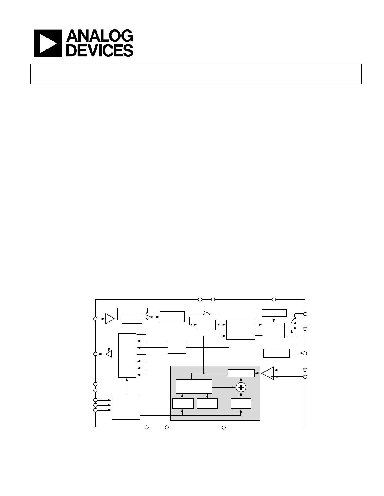
FUNCTIONAL BLOCK DIAGRAM
ADF4159
REF
IN
HIGH Z
CE
TXDATA
CLK
DATA
LE
Rev. PrC
Information furnished by Analog Devices is believed to be accurate and reliable. However, no
responsibility is assumed by Analog Devices for its use, nor for any infringements of patents or other
rights of third parties that may result from its use. Specifications subject to change without notice. No
license is granted by implication or otherwise under any patent or patent rights of Analog Devices.
Trademarks and registered trademarks are the property of their respective owners.
×2
DOUBLER
OUTPUT
MUX
32-BIT
DATA
REGISTER
V
DGND
SD
V
R
N
AGND
5-BIT
R COUNTER
DD
LOCK
DETECT
OUT
DD
DIV
DIV
THIRD-ORDER
FRACTIONAL
INTERPOLATOR
FRACTION
REG
DGND CPGND
÷2
DIVIDER
MODULUS
25
2
P
+
PHASE
FREQUENCY
DETECTOR
–
N COUNTER
INTEGER
REG
SET
REFERENCE
CHARGE
PUMP
FLO SWITCH
CSR
SW2
CP
SW1
RF
RF
IN
IN
Figure 1.
One Technology Way, P.O. Box 9106, Norwood, MA 02062-9106, U.S.A.
Tel: 781.329.4700 www.analog.com
Fax: 781.461.3113 ©2012 Analog Devices, Inc. All rights reserved.

ADF4159 Preliminary Technical Data
TABLE OF CONTENTS
Features .............................................................................................. 1
Applications ....................................................................................... 1
General Description ......................................................................... 1
LSB FRAC Register (R1) Map ................................................... 14
R-Divider Register (R2) Map .................................................... 16
Function Register (R3) Map...................................................... 18
Functional Block Diagram .............................................................. 1
Specifications ..................................................................................... 3
Timing Specifications .................................................................. 4
Absolute Maximum Ratings ............................................................ 6
ESD Caution .................................................................................. 6
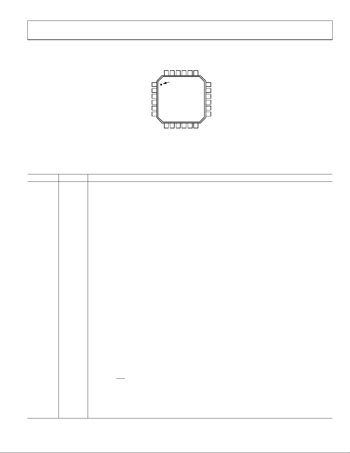
Pin Configuration and Pin Function Descriptions ...................... 7
Typical Performance Characteristics ............................................. 8
Reference Input Section ............................................................... 9
RF Input Stage ............................................................................... 9
RF INT Divider ............................................................................. 9
25-Bit Fixed Modulus .................................................................. 9
INT, FRAC, and R Relationship ................................................. 9
R-Counter ...................................................................................... 9
Phase Frequency Detector (PFD) and Charge Pump ............ 10
MUXOUT and LOCK Detect ................................................... 10
Input Shift Registers ................................................................... 10
Program Modes .......................................................................... 10
Register Maps .................................................................................. 11
FRAC/INT Register (R0) Map .................................................. 13
Test Register (R4) Map .............................................................. 20
Deviation Register (R5) Map .................................................... 21
Step Register (R6) Map .............................................................. 22
Delay Register (R7) Map ........................................................... 23
Applications Information .............................................................. 24
Initialization Sequence............................................................... 24
RF Synthesizer: A Worked Example ......................................... 24
Reference Doubler and Reference Divider ............................. 24
Cycle Slip Reduction for Faster Lock Times ........................... 24
Modulation .................................................................................. 25
Waveform Generation ............................................................... 25
Other Waveforms ....................................................................... 27
Fast Lock Mode........................................................................... 31
Spur Mechanisms ....................................................................... 32
Filter Design—ADIsimPLL ....................................................... 32
PCB Design Guidelines for the Chip Scale Package .............. 32
Application of ADF4159 in FMCW Radar.................................. 33
Outline Dimensions ....................................................................... 34
Rev. PrC | Page 2 of 35

Preliminary Technical Data ADF4159
SET
INL
INH/IINL
SPECIFICATIONS
AVDD = 2.7 V to 3.3 V, DVDD = SDVDD = 1.8V; VP = AVDD, AGND = DGND = 0 V, TA = T
MIN
to T
, dBm referred to 50 Ω, unless
MAX
otherwise noted.
Table 1.
C Version1
Parameter Min Typ Max Unit Test Conditions/Comments
RF CHARACTERISTICS
RF Input Frequency (RFIN) 0.5 13 GHz −10 dBm min to 0 dBm max; for lower frequencies, ensure
slew rate (SR) > 400 V/µs
REFERENCE CHARACTERISTICS
REFIN Input Frequency 10 260 MHz For f < 10 MHz, use a dc-coupled CMOS-compatible
square wave, slew rate > 25 V/µs
TBD MHz If an internal reference doubler is enabled
REFIN Input Sensitivity TBD V p-p Biased at 1.8/22
REFIN Input Capacitance 10 pF
REFIN Input Current ±100 µA
PHASE DETECTOR
Phase Detector Frequency3 110 MHz
CHARGE PUMP
ICP Sink/Source Programmable
High Value 5 mA With R
= 5.1 kΩ
SET
Low Value 312.5 µA
Absolute Accuracy 2.5 % With R
R
Range 2.7 10 kΩ
= 5.1 kΩ
SET
ICP Three-State Leakage Current 1 nA Sink and source current
Matching 2 % 0.5 V < VCP < VP – 0.5 V
ICP vs. VCP 2 % 0.5 V < VCP < VP – 0.5 V
ICP vs. Temperature 2 % VCP = VP/2
LOGIC INPUTS
V
, Input High Voltage 1.4 V
INH
V
, Input Low Voltage 0.6 V
I
, Input Current ±1 µA
CIN, Input Capacitance 10 pF
LOGIC OUTPUTS
VOH, Output High Voltage 1.4 V Open-drain output chosen; 1 kΩ pull-up to 1.8 V
VOH, Output High Voltage VDD − 0.4 V CMOS output chosen
IOH, Output High Current 100 µA
VOL, Output Low Voltage 0.4 V IOL = 500 µA
POWER SUPPLIES
AVDD 2.7 3.3 V
DVDD 1.6 1.8 2 V
SDVDD 1.6 1.8 2 V
VP 2.7 3.3 V
IDD 33 42 mA
Rev. PrC | Page 3 of 35
ADF4159 Preliminary Technical Data
1_f
t4t
Parameter Min Typ Max Unit Test Conditions/Comments
NOISE CHARACTERISTICS
Normalized Phase Noise Floor4 TBD dBc/Hz PLL loop BW = 500 kHz
Normalized 1/f Noise (PN
)5 TBD Measured at 10 kHz offset, normalized to 1 GHz
Phase Noise Performance6 @ VCO output
12000 MHz Output7 TBD dBc/Hz @ 50 kHz offset, 100 MHz PFD frequency
1
Operating temperature for C version: −40°C to +125°C.
2
AC-coupling ensures 1.8/2 bias.
3
Guaranteed by design. Sample tested to ensure compliance.
4
This figure can be used to calculate phase noise for any application. Use the formula TBD + 10 log(f
at the VCO output.
5
The PLL phase noise is composed of 1/f (flicker) noise plus the normalized PLL noise floor. The formula for calculating the 1/f noise contribution at an RF frequency, FRF,
and at an offset frequency, f, is given by PN = P
6
The phase noise is measured with the EVAL-ADF4159EB1Z and the Agilent E5052A phase noise system.
7
fREFIN = 100 MHz; fPFD = 100 MHz; offset frequency = 50 kHz; RFOUT = 12000 MHz; N = 120; loop bandwidth = 200 kHz.
TIMING SPECIFICATIONS
AVDD = 2.7 V to 3.3 V; DVDD = SDVDD = 1.8V; VP = AVDD; AGND = DGND = SDGND = 0V; TA = T
unless otherwise noted.
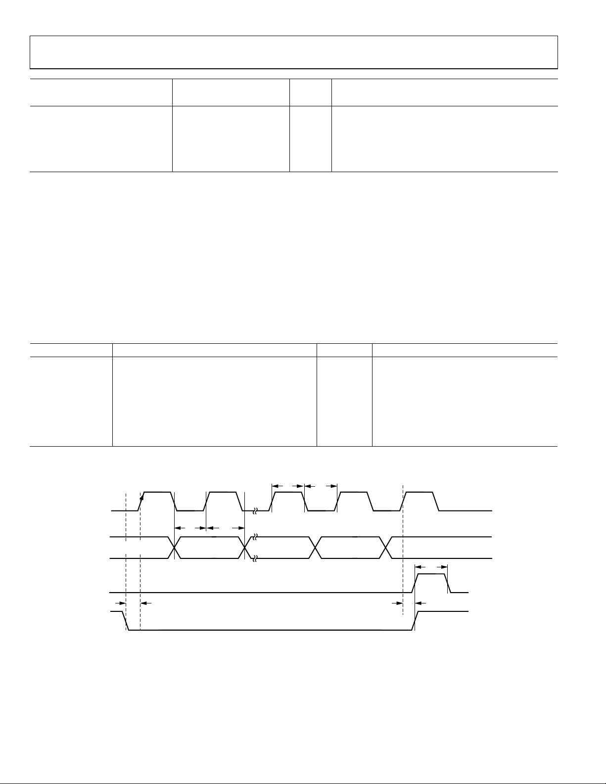
Table 2. Write Timing
Parameter Limit at T
t1 20 ns min LE setup time
t2 10 ns min DATA to CLK setup time
t3 10 ns min DATA to CLK hold time
t4 25 ns min CLK high duration
t5 25 ns min CLK low duration
t6 10 ns min CLK to LE setup time
t7 20 ns min LE pulse width
MIN
to T
MAX
C Version1
+ 10 log(10 kHz/f) + 20 log(FRF/1 GHz). Both the normalized phase noise floor and flicker noise are modeled in ADIsimPLL.
1_f
) + 20 logN to calculate in-band phase noise performance as seen
PFD
to T
MIN
, dBm referred to 50 Ω,
MAX
(C Version) Unit Test Conditions/Comments
Write Timing Diagram
CLK
DATA
LE
LE
t
2
DB31 (MSB) DB30
t
1
t
3
DB2
(CONTROL BIT C3)
Figure 2. Write Timing Diagram
Rev. PrC | Page 4 of 35
5
DB1
(CONTROL BIT C2)
DB0 (LSB)
(CONTROL BIT C1)
t
7
t
6
08728-026
Preliminary Technical Data ADF4159
DATA
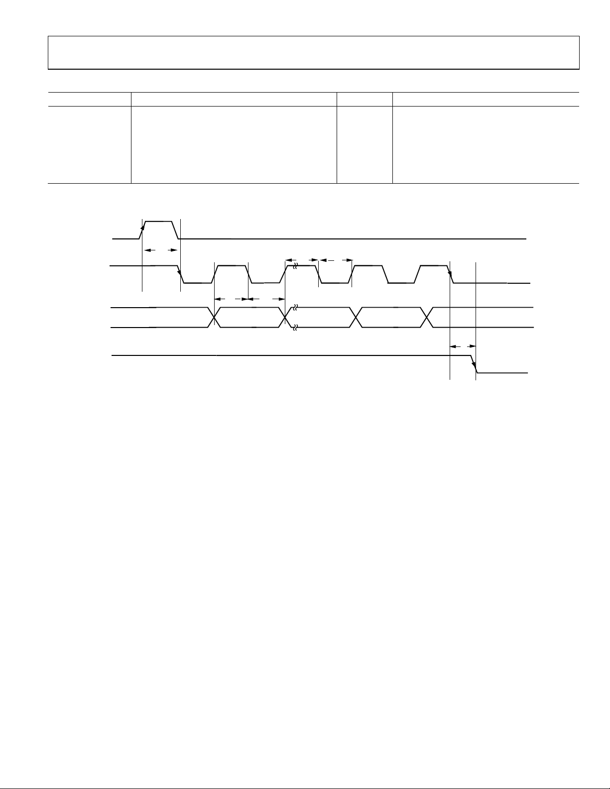
Table 3. Read Timing
Parameter Limit at T
t1 20 ns min TX
t2 10 ns min DATA (on MUXOUT) to CLK setup time
t3 10 ns min DATA (on MUXOUT) to CLK hold time
t4 25 ns min CLK high duration
t5 25 ns min CLK low duration
t6 10 ns min CLK to LE setup time
Read Timing Diagram
TXDATA
CLK
to T
MIN
(C Version) Unit Test Conditions/Comments
MAX
setup time
t
1
t
4
t
5
MUXOUT
LE
t
2
DB36 DB35
t
3
Figure 3. Read Timing Diagram
DB1DB2
DB0
t
6
08728-026
Rev. PrC | Page 5 of 35
ADF4159 Preliminary Technical Data
ABSOLUTE MAXIMUM RATINGS
TA = 25°C, GND = AGND = DGND = SDGND = 0 V,
VDD = AVDD , DVDD = SDVDD, unless otherwise noted.
Table 4.
Parameter Rating
AVDD to GND −0.3 V to +4 V
DVDD to GND −0.3 V to +2.4 V
VP to GND −0.3 V to +4 V
VP to AVDD −0.3 V to +0.6 V
Digital I/O Voltage to GND −0.3 V to VDD + 0.3 V
Analog I/O Voltage to GND −0.3 V to VDD + 0.3 V
REFIN, RFIN to GND −0.3 V to VDD + 0.3 V
Operating Temperature Range
Industrial (C Version) −40°C to +125°C
Storage Temperature Range −65°C to +125°C
Maximum Junction Temperature 150°C
LFCSP θJA Thermal Impedance
(Paddle Soldered)
Reflow Soldering
Peak Temperature 260°C
Time at Peak Temperature 40 sec
30.4°C/W
Stresses above those listed under Absolute Maximum Ratings
may cause permanent damage to the device. This is a stress
rating only; functional operation of the device at these or any
other conditions above those indicated in the operational
section of this specification is not implied. Exposure to absolute
maximum rating conditions for extended periods may affect
device reliability.
ESD CAUTION
Rev. PrC | Page 6 of 35
Preliminary Technical Data ADF4159
T
DD
5.25
PIN CONFIGURATION AND PIN FUNCTION DESCRIPTIONS
SETVP
CP24
R
232221
PIN1
1
CPGND
AGND 2
AGND
RFINB 4
RFINA 5
AV
DD
NOTES
1. THE LFCSP HAS AN EXPOSED PADDLE
THAT MUST BE CONNECTED TO GND.
3
6
IDENTIFIER
ADF4159
TOPVIEW
(Not to Scale)
789
IN
DD
DD
REF
AV
AV
DV
SW2
SW1
20
19
18
SDV
DD
17
MUXOU
16
LE
15
DATA
14
CLK
CE13
10
11
12
DATA
DGND
TX
SDGND
Figure 4. LFCSP Pin Configuration
Table 5. Pin Function Descriptions
Pin No. Mnemonic Description
1 CPGND Charge Pump Ground. This is the ground return path for the charge pump.
2, 3 AGND Analog Ground. This is the ground return path of the prescaler.
4 RFINB Complementary Input to the RF Prescaler. Decouple this point to the ground plane with a small bypass capacitor,
typically 100 pF.
5 RFINA Input to the RF Prescaler. This small-signal input is normally ac-coupled from the VCO.
6, 7, 8 AVDD Positive Power Supply for the RF Section. Place decoupling capacitors to the ground plane as close as possible to this
pin.
9 REFIN Reference Input. This is a CMOS input with a nominal threshold of VDD/2 and an equivalent input resistance of 100 kΩ.
It can be driven from a TTL or CMOS crystal oscillator, or it can be ac-coupled.
10 DGND Digital Ground.
11 SDGND Digital Σ-Δ Modulator Ground. Ground return path for the Σ-Δ modulator.
12 TX
13 CE Chip Enable. A logic low on this pin powers down the device and puts the charge pump output into three-state mode.
14 CLK Serial Clock Input. This serial clock is used to clock in the serial data to the registers. The data is latched into the shift
15 DATA Serial Data Input. The serial data is loaded MSB first with the three LSBs being the control bits. This input is a high
16 LE Load Enable, CMOS Input. When LE is high, the data stored in the shift registers is loaded into one of the eight latches,
17 MUXOUT Multiplexer Output. This pin allows either the RF lock detect, the scaled RF, or the scaled reference frequency to be
18 SDVDD Power Supply Pin for the Digital Σ-Δ Modulator. This pin should be 1.8V. Place decoupling capacitors to the ground
19 DVDD Positive Power Supply for the Digital Section. Place decoupling capacitors to the digital ground plane as close as
20 , 21 SW1, SW2 Switches for Fast Lock.
22 VP Charge Pump Power Supply. This should be greater than or equal to VDD. The max value of VP is 3.3V.
23 R
24 CP Charge Pump Output. When enabled, this provides ±ICP to the external loop filter, which in turn drives the external VCO.
25 EPAD Exposed Paddle. The LFCSP has an exposed paddle that must be connected to GND.
Tx Data Pin. Provide data to be transmitted in FSK or PSK mode on this pin.
DATA
register on the CLK rising edge. This input is a high impedance CMOS input.
impedance CMOS input.
with the latch being selected using the control bits.
accessed externally.
plane as close as possible to this pin.
possible to this pin. DVDD must be 1.8V.
Connecting a resistor between this pin and ground sets the maximum charge pump output current. The relationship
SET
between ICP and R
I
CPmax
R
SET
is
SET
where:
I
= 5 mA.
CPmax
R
= 5.1 kΩ.
SET
Rev. PrC | Page 7 of 35

ADF4159 Preliminary Technical Data
TYPICAL PERFORMANCE CHARACTERISTICS
TBD
Figure 5.
TBD
TBD
Figure 8
TBD
Figure 6
TBD
Figure 7.
Rev. PrC | Page 8 of 35
TBD
Figure 9.
Figure 10
Preliminary Technical Data ADF4159
POWER-DOWN
08728-016
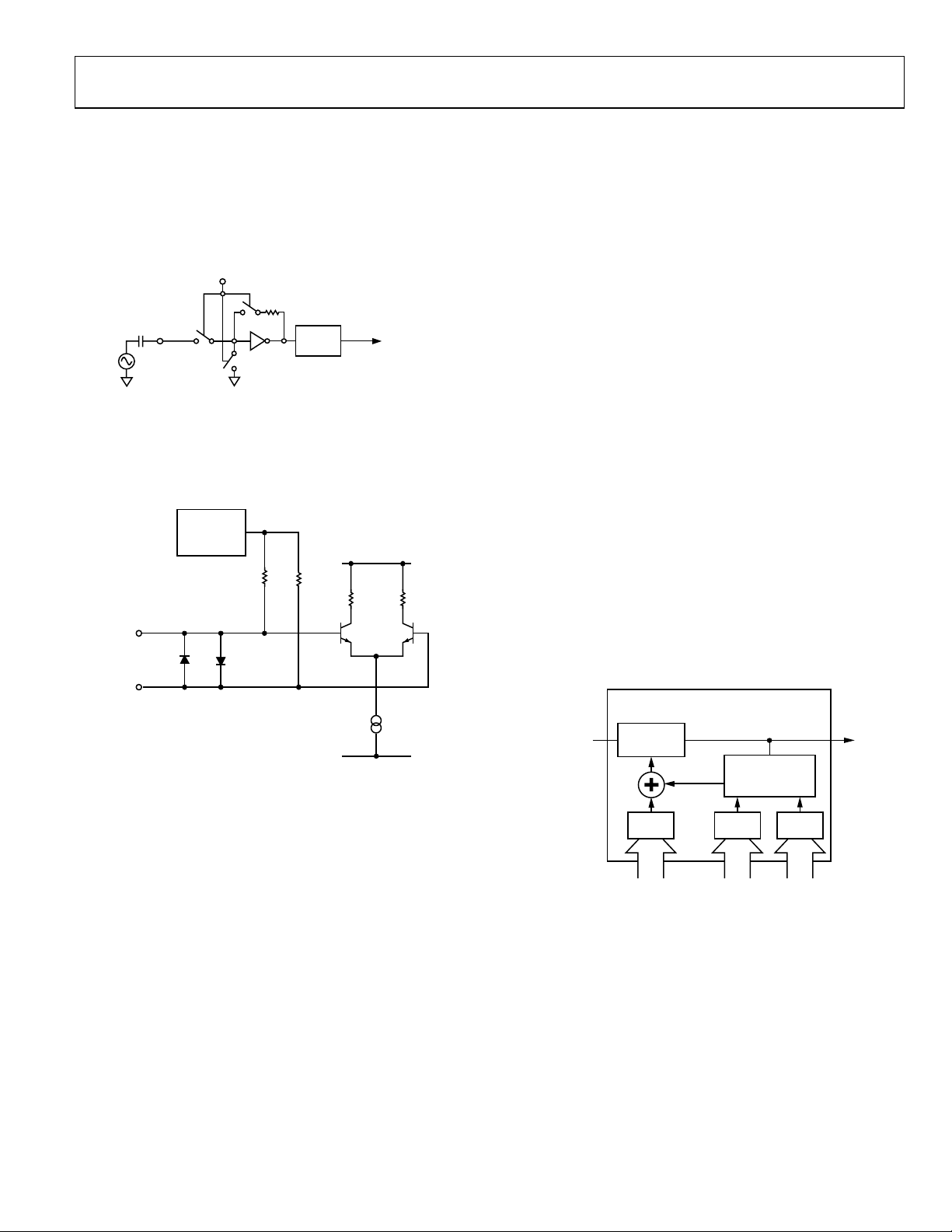
REFERENCE INPUT SECTION
The reference input stage is shown in Figure 11. SW1 and SW2
are normally closed switches. SW3 is normally open. When
power-down is initiated, SW3 is closed and SW1 and SW2 are
opened. This ensures that there is no loading of the REFIN pin
on power-down.
CONTROL
25-BIT FIXED MODULUS
The ADF4159 has a 25-bit fixed modulus. This allows output
frequencies to be spaced with a resolution of
f
= f
RES
where f
(PFD). For example, with a PFD frequency of 10 MHz,
frequency steps of 0.298 Hz are possible.
/225 (1)
PFD
is the frequency of the phase frequency detector
PFD
100kΩ
NC
REF
IN
NC
SW2
SW1
SW3
NO
Figure 11. Reference Input Stage
BUFFER
TO R-COUNTER
08728-027
RF INPUT STAGE
The RF input stage is shown in Figure 12. It is followed by a
2-stage limiting amplifier to generate the current-mode logic
(CML) clock levels needed for the prescaler.
1.6V
2kΩ 2kΩ
AV
DD
AGND
RFINA
RFINB
BIAS
GENERATOR
Figure 12. RF Input Stage
INT, FRAC, AND R RELATIONSHIP
The INT and FRAC values, in conjunction with the R-counter,
make it possible to generate output frequencies that are spaced
by fractions of the phase frequency detector (PFD). The RF
VCO frequency (RF
RF
= f
OUT
PFD
where:
RF
is the output frequency of external voltage controlled
OUT
oscillator (VCO).
INT is the preset divide ratio of binary 12-bit counter (23 to 4095).
FRAC is the numerator of the fractional division (0 to 225 − 1).
f
= REFIN × [(1 + D)/(R × (1 + T))] (3)
PFD
where:
REFIN is the reference input frequency.
D is the REFIN doubler bit (0 or 1).
T is the REFIN divide-by-2 bit (0 or 1).
R is the preset divide ratio of the binary, 5-bit, programmable
reference counter (1 to 32).
FROM RF
INPUT STAGE
08728-015
) equation is
OUT
× (INT + (FRAC/225)) (2)
RF N-DIVIDER
N-COUNTER
N = INT + FRAC/MOD
THIRD-ORDER
FRACTIONAL
INTERPOLATOR
TO PFD
RF INT DIVIDER
The RF INT CMOS counter allows a division ratio in the PLL
feedback counter. Division ratios from 23 to 4095 are allowed.
Rev. PrC | Page 9 of 35
INT
REG
Figure 13. RF N-Divider
MOD
REG
FRAC
VALUE
R-COUNTER
The 5-bit R-counter allows the input reference frequency
(REFIN) to be divided down to produce the reference clock
to the PFD. Division ratios from 1 to 32 are allowed.
ADF4159 Preliminary Technical Data
+IN
MUXOUT
PHASE FREQUENCY DETECTOR (PFD) AND
CHARGE PUMP
The PFD takes inputs from the R-counter and N-counter and
produces an output proportional to the phase and frequency
difference between them. Figure 14 shows a simplified schematic of the PFD. The PFD includes a fixed delay element that
sets the width of the antibacklash pulse, which is typically 3 ns.
This pulse ensures that there is no dead zone in the PFD transfer
function and gives a consistent reference spur level.
HIGH
HIGH
–IN
UP
Q1D1
U1
CLR1
DELAY
CLR2
DOWN
Q2D2
U2
Figure 14. PFD Simplified Schematic
U3
CHARGE
PUMP
CP
08728-017
MUXOUT AND LOCK DETECT
The output multiplexer on the ADF4159 allows the user
to access various internal points on the chip. The state of
MUXOUT is controlled by the M4, M3, M2, and M1 bits
(see Figure 18). Figure 15 shows the MUXOUT section in
block diagram form.
DV
THREE-STATE OUTPUT
DV
DD
DGND
R DIVIDER OUTPUT
N DIVIDER OUTPUT
DIGITAL LOCK DETECT
CLK DIVIDER OUTPUT
R DIVIDER/2
N DIVIDER/2
READBACK
MUX
Figure 15. MUXOUT Schematic
CONTROL
DD
DGND
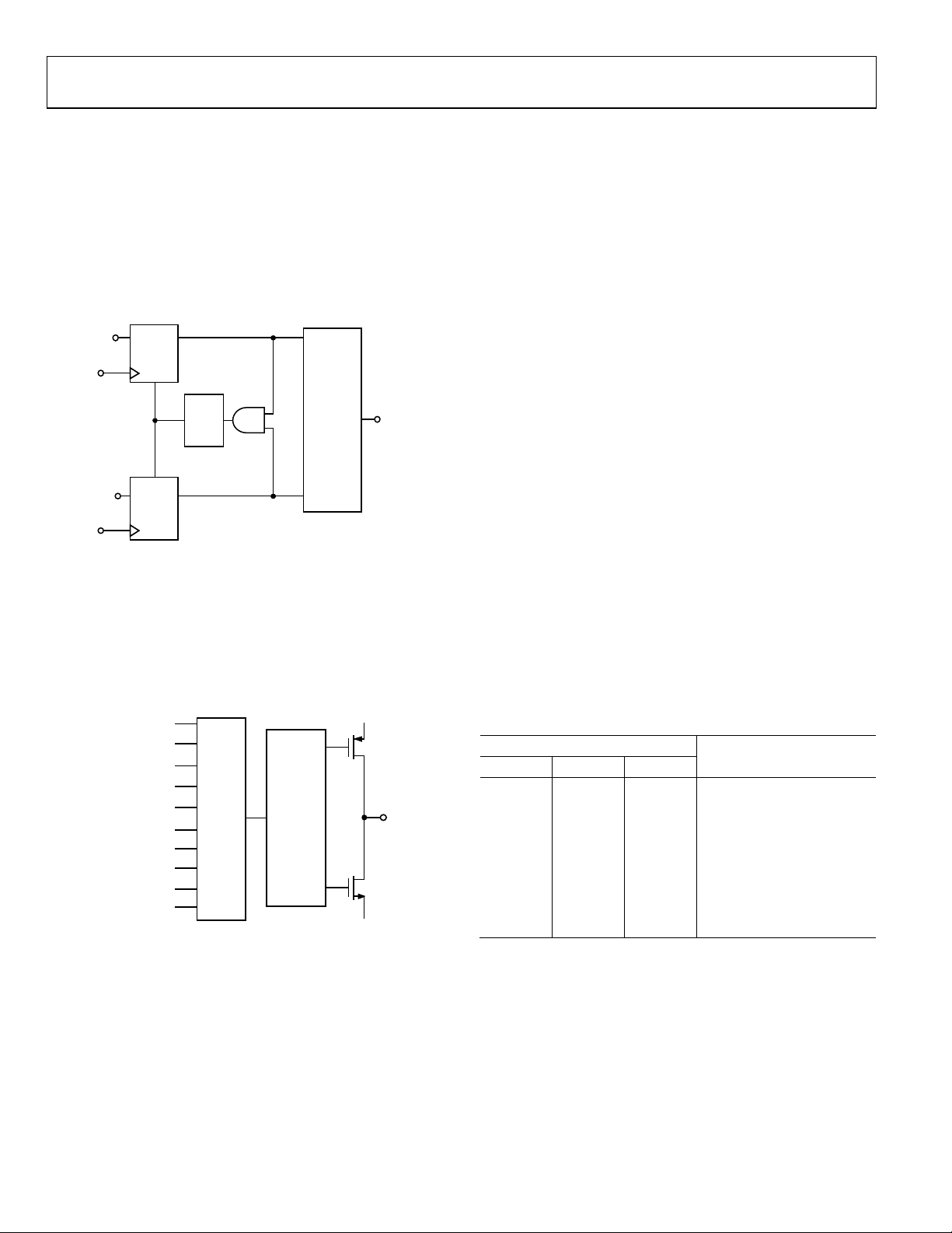
INPUT SHIFT REGISTERS
The ADF4159 digital section includes a 5-bit RF R-counter,
a 12-bit RF N-counter, and a 25-bit FRAC counter. Data is
clocked into the 32-bit shift register on each rising edge of
CLK. The data is clocked in MSB first. Data is transferred
from the shift register to one of eight latches on the rising edge
of LE. The destination latch is determined by the state of the
three control bits (C3, C2, and C1) in the shift register. These
are the three LSBs—DB2, DB1, and DB0—as shown in Figure 2.
The truth table for these bits is shown in Table 6. Figure 16 and
Figure 17 show a summary of how the latches are programmed.
PROGRAM MODES
Table 6 and Figure 18 through Figure 25 show how to set up
the program modes in the ADF4159.
Several settings in the ADF4159 are double buffered. These
include the LSB fractional value, R-counter value, reference
doubler, current setting, and RDIV2. This means that two
events must occur before the part uses a new value for any
of the double-buffered settings. First, the new value is latched
into the device by writing to the appropriate register. Second,
a new write must be performed on Register R0.
For example, updating the fractional value can involve a write
to the 13 LSB bits in R1 and the 12 MSB bits in R0. R1 should
be written to first, followed by the write to R0. The frequency
change begins after the write to R0. Double buffering ensures
that the bits written to in R1 do not take effect until after
the write to R0.
Table 6. C3, C2, and C1 Truth Table
Control Bits
C3 C2 C1 Register
0 0 0 R0
0 0 1 R1
0 1 0 R2
0 1 1 R3
1 0 0 R4
1 0 1 R5
1 1 0 R6
1 1 1 R7
Rev. PrC | Page 10 of 35
Preliminary Technical Data ADF4159
C1(0)
FRAC/INT REGISTER (R0)
C1(1)
C1(1)
C1(0)
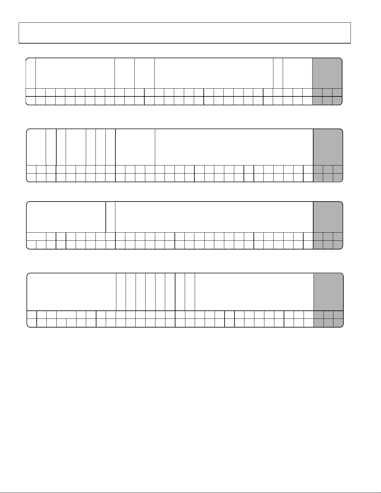
REGISTER MAPS
MUXOUT
CONTROL
RAMP ON
DB31
DB30 DB29 DB28 DB27 DB26 DB25 DB24 DB23 DB22 DB21 DB20 DB19 DB18 DB17 DB16 DB15 DB14 DB13 DB12 DB11 DB10 DB9 DB8 DB7 DB6 DB5 DB4 DB3 DB2 DB1 DB0
R1 M4 M3 M2 M1 N12 N11 N10 N9 N8 N7 N6 N5 N4 N3 N2 N1 F25 F24 F23 F22 F21 F20 F19 F18 F17 F16 F15 F14 C3(0) C2(0)
12-BIT INTEGER VALUE (INT)
12-BIT MSB FRACTIONAL VALUE
(FRAC)
CONTROL
BITS
LSB FRAC REGISTER (R1)
RESERVED
PHASE ADJ
DB31
DB30 DB29 DB28 DB27 DB26 DB25 DB24 DB23 DB22 DB21 DB20 DB19 DB18 DB17 DB16 DB15 DB14 DB13 DB12 DB11 DB10 DB9 DB8 DB7 DB6 DB5 DB4 DB3 DB2 DB1 DB0
0 0 0 P1 F13 F12 F11 F10 F9 F8 F7 F6 F5 F4 F3 F2 F1 0 0 0 0 0 0 0 0 0 0 0 0 C3(0) C2(0)
13-BIT LSB FRACTIONAL VALUE
(FRAC) (DBB)
12-BIT PHASE WORD
(DBB)
CONTROL
BITS
R DIVIDER REGISTER (R2)
DBB DBB
CURRENT
SETTING
RESERVED
DB31
DB30 DB29 DB28 DB27 DB26 DB25 DB24 DB23 DB22 DB21 DB20 DB19 DB18 DB17 DB16 DB15 DB14 DB13 DB12 DB11 DB10 DB9 DB8 DB7 DB6 DB5 DB4 DB3 DB2 DB1 DB0
0 0 0 C1 CPI4 CPI3 CPI2 CPI1 0 P1 U2 U1 R5 R4 R3 R2 R1 D12 D11 D10 D9 D8 D7 D6 D5 D4 D3 D2 D1 C3(0) C2(1)
CSR EN
RESERVED
RDIV2 DBB
PRESCALER
5-BIT R COUNTER
REFERENCE
DOUBLER DBB
12-BIT MOD DIVIDER
(DBB)
CONTROL
BITS
FUNCTION REGISTER (R3)
RESERVED
RESERVED
DB31
DB30 DB29 DB28 DB27 DB26 DB25 DB24 DB23 DB22 DB21 DB20 DB19 DB18 DB17 DB16 DB15 DB14 DB13 DB12 DB11 DB10 DB9 DB8 DB7 DB6 DB5 DB4 DB3 DB2 DB1 DB0
0 0 0 0 0 0 0 0 0 0 0 0 0 0 1 L1 NS1 U12 0 0 RM2 RM1 PE1 FE1 U11 U10 U9 U8 U7 C3(0) C2(1)
NOTES
1. DBB = DOUBLE BUFFERED BIT(S).
SD
RESET
N SEL
LOL EN
RESERVED
RAMP MODE
PSK ENABLE
LDP
FSK ENABLE
Figure 16. Register Summary 1
PD
PD
CP
RESET
POLARITY
COUNTER
THREE-STATE
CONTROL
BITS
Rev. PrC | Page 11 of 35
ADF4159 Preliminary Technical Data
C1(1)
TEST REGISTER (R4)
READ
RESERVED RESERVED
LE SEL
DB31
DB30 DB29 DB28 DB27 DB26 DB25 DB24 DB23 DB22 DB21 DB20 DB19 DB18 DB17 DB16 DB15 DB14 DB13 DB12 DB11 DB10 DB9 DB8 DB7 DB6 DB5 DB4 DB3 DB2 DB1 DB0
LS1 0 0 0 0 0 0 0 0 R2 R1 C2 C1 D12 D11 D10 D9 D8 D7 D6 D5 D4 D3 D2 D1 C3(1) C2(0) C1(0)
BACK
MUXOUT
TO
CLK
DIV
MODE
12-BIT CLOCK DIVIDER VALUE
CS1
CONTROL
BITS
CLK DIV SEL
0 0
0
DEV REGISTER (R5)
4-BIT DEV OFFSET
WORD
RESERVED
TX RAMP CLK
DB31
DB30 DB29 DB28 DB27 DB26 DB25 DB24 DB23 DB22 DB21 DB20 DB19 DB18 DB17 DB16 DB15 DB14 DB13 DB12 DB11 DB10 DB9 DB8 DB7 DB6 DB5 DB4 DB3 DB2 DB1 DB0
0 0 TR1 PR1 I2 I1 FRE1 R2E1 DS1 DO4 DO3 DO2 DO1 D16 D15 D14 D13 D12 D11 D10 D9 D8 D7 D6 D5 C3(1) C2(0) C1(0)
PAR RAMP
INTERRUPT
RAMP 2 EN
FSK RAMP EN
DEV SEL
16-BIT DEVIATION WORD
D4
D2 D1
D3
CONTROL
BITS
STEP REGISTER (R6)
RESERVED
STEP SEL
DB31
DB30 DB29 DB28 DB27 DB26 DB25 DB24 DB23 DB22 DB21 DB20 DB19 DB18 DB17 DB16 DB15 DB14 DB13 DB12 DB11 DB10 DB9 DB8 DB7 DB6 DB5 DB4 DB3 DB2 DB1 DB0
0 0 0 0 0 0 0 0 SSE1 S20 S19 S18 S17 S16 S15 S14 S13 S12 S11 S10 S9 S8 S7 S6 S5 S4 S3 S2 S1 C3(0) C2(0) C1(0)
20-BIT STEP WORD
CONTROL
BITS
DELAY REGISTER (R7)
RESERVED
TRI DELAY
DB31
DB30 DB29 DB28 DB27 DB26 DB25 DB24 DB23 DB22 DB21 DB20 DB19 DB18 DB17 DB16 DB15 DB14 DB13 DB12 DB11 DB10 DB9 DB8 DB7 DB6 DB5 DB4 DB3 DB2 DB1 DB0
0 0 0 0 0 0 0 0 0 TD1 ST1 TR1 FR1 RDF1 RD1 DC1 DSE1 DS12 DS11 DS10 DS9 DS8 DS7 DS6 DS5 DS4 DS3 DS2 DS1 C3(0) C2(0)
TX RB EN
SING FULL TRI
FAST RAMP
RAMP DEL
DEL CLK SEL
RAMP DEL FL
DEL START EN
Figure 17. Register Summary 2
12-BIT DELAY START DIVIDER
CONTROL
BITS
Rev. PrC | Page 12 of 35

Preliminary Technical Data ADF4159
FRAC/INT REGISTER (R0) MAP
With Register R0 DB[2:0] set to [0, 0, 0], the on-chip
FRAC/INT register is programmed as shown in Figure 18.
Ramp On
Setting DB31 to 1 enables the ramp, setting DB31 to 0 disables
the ramp.
MUXOUT Control
The on-chip multiplexer is controlled by DB[30:27] on the
ADF4159. See Figure 18 for the truth table.
12-Bit Integer Value (INT)
These 12 bits control what is loaded as the INT value. This is
used to determine the overall feedback division factor. It is used
in Equation 2. See the INT, FRAC, and R Relationship section
on Page 9 for more information.
12-Bit MSB Fractional Value (FRAC)
These 12 bits, along with Bits DB[27:15] in the LSB FRAC
register (Register R1), control what is loaded as the FRAC value
into the fractional interpolator. This is part of what determines
the overall feedback division factor. It is also used in Equation 2.
These 12 bits are the most significant bits (MSB) of the 25-bit
FRAC value, and Bits DB[27:15] in the LSB FRAC register
(Register R1) are the least significant bits (LSB). See the RF
Synthesizer: A Worked Example section on Page 23 for more
information.
Rev. PrC | Page 13 of 35

ADF4159 Preliminary Technical Data
MUXOUT
CONTROL
RAMP ON
DB31
DB30 DB29 DB28 DB27 DB26 DB25 DB24 DB23 DB22 DB21 DB20 DB19 DB18 DB17 DB16 DB15 DB14 DB13 DB12 DB11 DB10 DB9 DB8 DB7 DB6 DB5 DB4 DB3 DB2 DB1 DB0
R1 M4 M3 M2 M1 N12 N11 N10 N9 N8 N7 N6 N5 N4 N3 N2 N1 F25 F24 F23 F22 F21 F20 F19 F18 F17 F16 F15 F14 C3(0) C2(0) C1(0)
R1 RAMP ON
0 RAMP DISABLED
RAMP ENABLED1
M4 M3 M2 M1 OUTPUT
0 0 0 0 THREE-STATE OUTPUT
0 0 0 1 DV
0 0 1 0 DGND
0 0 1 1 R-DIVIDER OUTPUT
0 1 0 0 N-DIVIDER OUTPUT
0 1 0 1 RESERVED
0 1 1 0 DIGITAL LOCK DETECT
0 1 1 1 SERIAL DATA OUTPUT
1 0 0 0 RESERVED
1 0 0 1 RESERVED
1 0 1 0 CLK DIVIDER OUTPUT
1 0 1 1 RESERVED
1 1 0 0 FAST-LOCK SWITCH
1 1 0 1 R-DIVIDER/2
1 1 1 0 N-DIVIDER/2
1 1 1 1 READBACK TO MUXOUT
12-BIT INTEGER VALUE (INT)
DD
N12 N11 N10 N9 N8 N7 N6 N5 N4 N3 N2 N1
0 0 0 0 0 0 0 1 0 1 1 1 23
0 0 0 0 0 0 0 1 1 0 0 0 24
0 0 0 0 0 0 0 1 1 0 0 1 25
0 0 0 0 0 0 0 1 1 0 1 0 26
. . . . . . . . . . . . .
. . . . . . . . . . . . .
. . . . . . . . . . . . .
1 1 1 1 1 1 1 1 1 1 0 1 4093
1 1 1 1 1 1 1 1 1 1 1 0 4094
1 1 1 1 1 1 1 1 1 1 1 1 4095
Figure 18. FRAC/INT Register (R0) Map
LSB FRAC REGISTER (R1) MAP
With Register R1 DB[2:0] set to [0, 0, 1], the on-chip LSB FRAC
register is programmed as shown in Figure 19.
Phase Adj
This bit enables /disables phase adjustment. Phase of the
generated signal is adjusted by the value programmed by bits
DB[14:3] in Register R1 (12-bit Phase Value).
13-Bit LSB FRAC Value
These 13 bits, along with Bits DB[14:3] in the FRAC/INT
register (Register R0), control what is loaded as the FRAC value
into the fractional interpolator. This is part of what determines
the overall feedback division factor. It is also used in Equation 2.
These 13 bits are the least significant bits (LSB) of the 25-bit
12-BIT MSB FRACTIONAL VALUE
F25 F24 .......... F15 F14
0 0 .......... 0 0 0
0 0 .......... 0 1 1
0 0 .......... 1 0 2
0 0 .......... 1 1 3
. . .......... . . .
. . .......... . . .
. . .......... . . .
1 1 .......... 0 0 4092
1 1 .......... 0 1 4093
1 1 .......... 1 0 4094
1 1 .......... 1 1 4095
*THE FRAC VALUE IS MADE UP OF THE 12-BIT MSB STORED IN
REGISTER R0, AND THE 13-BIT LSB REGISTER STORED IN
REGISTER R1. FRAC VALUE = 13-BIT LSB + 12-BIT MSB × 213.
(FRAC)
INTEGER VALUE
(INT)
MSB FRACTIONAL VALUE
(FRAC)*
CONTROL
BITS
08728-011
FRAC value, and Bits DB[14:3] in the INT/FRAC register are
the most significant bits (MSB). See the RF Synthesizer: A
Worked Example section on Page 23 for more information.
12-Bit Phase Value
These twelve bits control what is loaded as the PHASE word.
The word is used to program the RF output phase from 0° to
360 o with a resolution of 360o/212. The phase shift equals to
120
2/360PhaseValue . If the PHASE ADJUSTMENT is
not being used, it is recommended that the PHASE word be set
to 0.
Reserved Bits
All reserved bits should be set to 0 for normal operation.
Rev. PrC | Page 14 of 35

Preliminary Technical Data ADF4159
C1(1)
P1 PHASE ADJ
0 DISABLED
1 ENABLED
RESERVED
DB31
DB30 DB29 DB28 DB27 DB26 DB25 DB24 DB23 DB22 DB21 DB20 DB19 DB18 DB17 DB16 DB15 DB14 DB13 DB12 DB11 DB10 DB9 DB8 DB7 DB6 DB5 DB4 DB3 DB2 DB1 DB0
0 0 0 P1 F13 F12 F11 F10 F9 F8 F7 F6 F5 F4 F3 F2 F1 P12 P11 P10 P9 P8 P7 P6 P5 P4 P3 P2 P1 C3(0) C2(0)
PHASE ADJ
F13 F12 .......... F2 F1
0 0 .......... 0 0 0
0 0 .......... 0 1 1
0 0 .......... 1 0 2
0 0 .......... 1 1 3
. . .......... . . .
. . .......... . . .
. . .......... . . .
1 1 .......... 0 0 8188
1 1 .......... 0 1 8189
1 1 .......... 1 0 8190
1 1 .......... 1 1 8191
*THE FRAC VALUE IS MADE UP OF THE 12-BIT MSB STORED IN
REGISTER 0, AND THE 13-BIT LSB REGISTER STORED IN
REGISTER 1. FRAC VALUE = 13-BIT LSB + 12-BIT MSB × 213.
13-BIT LSB FRACTIONAL VALUE
(FRAC) (DBB)
LSB FRACTIONAL VALUE
(FRAC)*
12-BIT PHASE VALUE
(DBB)
P12 P11 .......... P2 P1 PHASE VALUE (PHASE)
0 0 .......... 0 0 0
0 0 .......... 0 1 1 (RECOMMENDED)
0 0 .......... 1 0 2
0 0 .......... 1 1 3
. . .......... . . .
. . .......... . . .
. . .......... . . .
1 1 .......... 0 0 4092
1 1 .......... 0 1 4093
1 1 .......... 1 0 4094
1 1 .......... 1 1 4095
CONTROL
Figure 19. LSB FRAC Register (R1) Map
BITS
Rev. PrC | Page 15 of 35

ADF4159 Preliminary Technical Data
R-DIVIDER REGISTER (R2) MAP
With Register R2 DB[2:0] set to [0, 1, 0], the on-chip R-divider
register is programmed as shown in Figure 20.
Reserved Bits
All reserved bits should be set to 0 for normal operation.
CSR Enable
Setting this bit to 1 enables cycle slip reduction. This is a
method for improving lock times. Note that the signal at the PFD
must have a 50% duty cycle in order for cycle slip reduction to
work. In addition, the charge pump current setting must be set
to a minimum. See the Cycle Slip Reduction for Faster Lock
Times section on Page 23 for more information.
Also note that the cycle slip reduction feature can only be
operated when the phase detector polarity setting is positive
(DB6 in Register R3). It cannot be used if the phase detector
polarity is set to negative.
Charge Pump Current Setting
DB[27:24] set the charge pump current setting (see Figure 20).
Set these bits to the charge pump current that the loop filter is
designed with.
Prescaler (P/P + 1)
The dual-modulus prescaler (P/P + 1), along with the INT,
FRAC, and MOD counters, determines the overall division
ratio from the RFIN to the PFD input.
Operating at CML levels, it takes the clock from the RF input
stage and divides it down for the counters. It is based on
a synchronous 4/5 core. When set to 4/5, the maximum RF
frequency allowed is 3 GHz. Therefore, when operating
the ADF4159 above 3 GHz, the prescaler must be set to 8/9.
The prescaler limits the INT value.
With P = 4/5, N
With P = 8/9, N
MIN
MIN
= 23.
= 75.
RDIV2
Setting DB21 to 1 inserts a divide-by-2 toggle flip-flop between
the R-counter and the PFD. This can be used to provide a 50%
duty cycle signal at the PFD for use with cycle slip reduction.
Reference Doubler
Setting DB20 to 0 feeds the REFIN signal directly to the 5-bit RF
R-counter, disabling the doubler. Setting this bit to 1 multiplies
the REFIN frequency by a factor of 2 before feeding the signal
into the 5-bit R-counter. When the doubler is disabled, the
REFIN falling edge is the active edge at the PFD input to the
fractional synthesizer. When the doubler is enabled, both the
rising edge and falling edge of REFIN become active edges at the
PFD input.
The maximum allowed REFIN frequency when the doubler is
enabled is 30 MHz.
5-Bit R-Counter
The 5-bit R-counter allows the input reference frequency
(REFIN) to be divided down to produce the reference clock
to the phase frequency detector (PFD). Division ratios from
1 to 32 are allowed.
12-Bit MOD Divider
Bits DB[14:3] are used to program the MOD divider, which
determines the duration of the time step in ramp mode.
Rev. PrC | Page 16 of 35

Preliminary Technical Data ADF4159
08728-013
DBB DBB
CP
CURRENT
SETTING
RESERVED
DB31
DB30 DB29 DB28 DB27 DB26 DB25 DB24 DB23 DB22 DB21 DB20 DB19 DB18 DB17 DB16 DB15 DB14 DB13 DB12 DB11 DB10 DB9 DB8 DB7 DB6 DB5 DB4 DB3 DB2 DB1 DB0
0 0 0 CR1 CPI4 CPI3 CPI2 CPI1 0 P1 U2 U1 R5 R4 R3 R2 R1 D12 D11 D10 D9 D8 D7 D6 D5 D4 D3 D2 D1 C3(0) C2(1) C1(0)
CSR EN
RESERVED
REFERENCE
RDIV2 DBB
PRESCALER
DOUBLER DBB
12-BIT MOD DIVIDER5-BIT R COUNTER
CONTROL
BITS
CYCLE SLIP
CR1
REDUCTION
0 DISABLED
1 ENABLED
CPI4 CPI3 CPI2 CPI1 5.1kΩ
0 0 0 0 0.31
0 0 0 1 0.63
0 0 1 0 0.94
0 0 1 1 1.25
0 1 0 0 1.57
0 1 0 1 1.88
0 1 1 0 2.19
0 1 1 1 2.5
1 0 0 0 2.81
1 0 0 1 3.13
1 0 1 0 3.44
1 0 1 1 3.75
1 1 0 0 4.06
1 1 0 1 4.38
1 1 1 0 4.69
1 1 1 1 5
NOTES
1. DBB = DOUBLE-BUFFERED BITS.
ICP(mA)
U2 R DIVIDER
0 DISABLED
1 ENABLED
P1 PRESCALER
0 4/5
1 8/9
REFERENCE
U1
DOUBLER
0 DISABLED
1 ENABLED
R5 R4 R3 R2 R1 R-COUNTER DIVIDE RATIO
0 0 0 0 1 1
0 0 0 1 0 2
0 0 0 1 1 3
0 0 1 0 0 4
. . . . .
. . . . .
. . . . .
1 1 1 0 1 29
1 1 1 1 . 30
1 1 1 1 1 31
0 0 0 0 0 32
Figure 20. R-Divider Register (R2) Map
D12 D11 .......... D2 D1 12-BIT MOD DIVIDER VALUE
0 0 .......... 0 0 0
0 0 .......... 0 1 1
0 0 .......... 1 0 2
0 0 .......... 1 1 3
. . .......... . . .
. . .......... . . .
. . .......... . . .
1 1 .......... 0 0 4092
1 1 .......... 0 1 4093
1 1 .......... 1 0 4094
1 1 .......... 1 1 4095
Rev. PrC | Page 17 of 35

ADF4159 Preliminary Technical Data
FUNCTION REGISTER (R3) MAP
With Register R3 DB[2:0] set to [0, 1, 1], the on-chip function
register is programmed as shown in Figure 21.
Reserved Bits
All reserved bits should be set to 0 for normal operation.
Loss of Lock (LOL)
This bit enables/disables loss of lock indication. This setting
indicates loss of lock even in the case of removing the reference
which is a big advantage over the standard implementation of
lock detect.
N SEL
This setting is used to circumvent the issue of pipeline delay
between an update of the integer and fractional values in the
N-counter. Typically, the INT value is loaded first, followed by
the FRAC value. This can cause the N-counter value to be at an
incorrect value for a brief period of time equal to the pipeline
delay (about four PFD cycles). This has no effect if the INT
value has not been updated. However, if the INT value has been
changed, this can cause the PLL to overshoot in frequency while
it tries to lock to the temporarily incorrect N value. After the
correct fractional value is loaded, the PLL quickly locks to the
correct frequency. Introducing an additional delay to the loading of the INT value using the N SEL bit causes the INT and
FRAC values to be loaded at the same time, preventing frequency
overshoot. The delay is turned on by setting Bit DB15 to 1.
SD Reset
For most applications, DB14 should be set to 0. When DB14 is
set to 0, the Σ-Δ modulator is reset on each write to Register R0.
If it is not required that the Σ-Δ modulator be reset on each
Register R0 write, set this bit to 1.
Ramp Mode
DB[11:10] determine the type of generated waveform.
PSK Enable
When DB9 is set to 1, PSK modulation is enabled. When set to
0, PSK modulation is disabled.
FSK Enable
When DB8 is set to 1, FSK modulation is enabled. When set to
0, FSK modulation is disabled.
Lock Detect Precision (LDP)
When DB7 is programmed to 0, 24 consecutive PFD cycles of
15 ns must occur before digital lock detect is set. When this bit
is programmed to 1, 40 consecutive reference cycles of 15 ns
must occur before digital lock detect is set.
Phase Detector (PD) Polarity
DB6 sets the phase detector polarity. When the VCO
characteristics are positive, set this bit to 1. When the
VCO characteristics are negative, set this bit to 0.
Power-Down
DB5 provides the programmable power-down mode. Setting
this bit to 1 performs a power-down. Setting this bit to 0 returns
the synthesizer to normal operation. While in software powerdown mode, the part retains all information in its registers.
Only when supplies are removed are the register contents lost.
When a power-down is activated, the following events occur:
1. All active dc current paths are removed.
2. The synthesizer counters are forced to their load state
conditions.
3. The charge pump is forced into three-state mode.
4. The digital lock-detect circuitry is reset.
5. The RFIN input is debiased.
6. The input register remains active and capable of loading
and latching data.
Charge Pump Three-State
DB4 puts the charge pump into three-state mode when
programmed to 1. It should be set to 0 for normal operation.
Counter Reset
DB3 is the RF counter reset bit. When this bit is set to 1, the RF
synthesizer counters are held in reset. For normal operation, set
this bit to 0.
Rev. PrC | Page 18 of 35

Preliminary Technical Data ADF4159
RESERVED
RESERVED
DB31
DB30 DB29 DB28 DB27 DB26 DB25 DB24 DB23 DB22 DB21 DB20 DB19 DB18 DB17 DB16 DB15 DB14 DB13 DB12 DB11 DB10 DB9 DB8 DB7 DB6 DB5 DB4 DB3 DB2 DB1 DB0
0 0 0 0 0 0 0 0 0 0 0 0 0 0 1 L1 NS1 U12 0 0 RM2 RM1 PE1 FE1 U11 U10 U9 U8 U7 C3(0) C2(1) C1(1)
L1 LOL
0 DISABLED
1 ENABLED
NS1 N SEL
0 N WORD LOAD ON SDCLK
1 N WORD LOAD DELAYED 4 CYCLES
U12 SD RESET
0 ENABLED
1 DISABLED
RM2 RM1 RAMP MODE
0
0
1
1 1
SD
LOL
N SEL
RESET
RESERVED
RAMP MODE
PE1 PSK EN
0 DISABLED
1 ENABLED
FE1 FSK EN
0 DISABLED
1 ENABLED
U11 LDP
0 24 PFD CYCLES
1 40 PFD CYCLES
0 CONTINUOUS SAWTOOTH
1 CONTINUOUS TRIANGULAR
0
SINGLE SAWTOOTH BURST
SINGLE RAMP BURST
FSK EN
PSK EN
U10 PD POLARITY
PD
PD
LDP
POLARITY
U8CPTHREE-STATE
U9 POWER-DOWN
0 DISABLED
1 ENABLED
0 NEGATIVE
1 POSITIVE
CONTROL
CP
THREE-STATE
0 DISABLED
1 ENABLED
BITS
RESET
COUNTER
COUNTER
U7
RESET
0 DISABLED
1 ENABLED
Figure 21. Function Register (R3) Map
Rev. PrC | Page 19 of 35

ADF4159 Preliminary Technical Data
C1(0)
TEST REGISTER (R4) MAP
With Register R4 DB[2:0] set to [1, 0, 0], the on-chip test
register (R4) is programmed as shown in Figure 22.
LE SEL
In some applications, it is necessary to synchronize LE
with the reference signal. To do this, DB31 should be set
to 1. Synchronization is done internally on the part.
Reserved Bits
All reserved bits should be set to 0 for normal operation.
Readback to MUXOUT
DB[22:21] enable or disable the readback to MUXOUT
function. This function allows reading back the synthesizer’s
frequency at the moment of interrupt.
CLK DIV Mode
Depending on the settings of DB[20:19], the 12-bit clock
divider may be a counter for the switched R fast-lock ramp
(CLK2), or it may be turned off.
12-Bit Clock Divider Value
DB[18:7] program the clock divider, which is used as a timer for
ramp - CLK2, while operating in ramp mode. See Waveform
Deviations and Timing section on Page 25 for more details.The
timer also determines how long the loop remains in wideband
mode while the switched R fast-lock technique is used. See FastLock Timer and Register Sequences on Page 30 for more details.
CLK DIV Sel
DB[6] selects which clock divider is loaded with 12-BIT
CLOCK DIVIDER VALUE. It can be either clock divider one or
clock divider two. These setting is used in the Fast Ramp Mode
for programming the up and down ramp time step. Please see
the Fast Ramp Mode section on Page 28 for more details.
READ
RESERVED
LE SEL
DB31
DB30 DB29 DB28 DB27 DB26 DB25 DB24 DB23 DB22 DB21 DB20 DB19 DB18 DB17 DB16 DB15 DB14 DB13 DB12 DB11 DB10 DB9 DB8 DB7 DB6 DB5 DB4 DB3 DB2 DB1 DB0
LS1 0 0 0 0 0 0 0 0 R2 R1 C2 C1 D12 D11 D10 D9 D8 D7 D6 D5 D4 D3 D2 D1 C3(1) C2(0)
LS1 LE SEL
0 LE FROM PIN
1 LE SYNCH WITH REFB
R1
R2 READBACK TO MUXOUT
0 DISABLED
0
1
0
C2 C1 CLOCK DIVIDER MODE
0 0
0 1 FAST LOCK DIVIDER
1 0
1
BACK
MUXOUT
ENABLED
CLOCK DIVIDER OFF
RESERVED
RAMP DIVIDER
1
TO
CLK
DIV
MODE
12-BIT CLOCK DIVIDER VALUE
D12 D11 .......... D2 D1 CLOCK DIVIDER VALUE
0 0 .......... 0 0 0
0 0 .......... 0 1 1
0 0 .......... 1 0 2
0 0 .......... 1 1 3
. . .......... . . .
. . .......... . . .
. . .......... . . .
1 1 .......... 0 0 4092
1 1 .......... 0 1 4093
1 1 .......... 1 0 4094
1 1 .......... 1 1 4095
RESERVED
CLK DIV SEL
CS1 0
CS1 CLK DIV SEL
0 LOAD CLK DIV 1
LOAD CLK DIV 2
1
CONTROL
BITS
0
0
Figure 22. Test Register (R4) Map
Rev. PrC | Page 20 of 35

Preliminary Technical Data ADF4159
DEVIATION REGISTER (R5) MAP
With Register R5 DB[2:0] set to [1, 0, 1], the on-chip deviation
register is programmed as shown in Figure 23.
Reserved Bits
All reserved bits should be set to 0 for normal operation.
Tx Ramp CLK
Setting DB29 to 0 uses the clock divider clock for clocking the
ramp. Setting DB29 to 1 uses the Tx data clock for clocking
the ramp.
PAR Ramp
Setting DB28 to 1 enables the parabolic ramp. Setting DB28 to 0
disables the parabolic ramp.
Interrupt
DB[27:26] determine which type of interrupt is used. This
feature is used for reading back the INT and FARC value of a
ramp at a given moment in time (rising edge on the TX
pin triggers the interrupt). From these bits, frequency can be
obtained. After readback, the sweep might continue or stop
at the readback frequency.
DATA
FSK Ramp Enable
Setting DB25 to 1 enables the FSK ramp. Setting DB25 to 0
disables the FSK ramp.
Ramp 2 Enable
Setting DB24 to 1 enables the second ramp. Setting DB24 to 0
disables the second ramp.
Deviation Select
Setting DB23 to 0 chooses the first deviation word. Setting
DB23 to 1, chooses the second deviation word.
4-Bit Deviation Offset Word
DB[22:19] determine the deviation offset. The deviation offset
affects the deviation resolution.
16-Bit Deviation Word
DB[18:3] determine the signed deviation word. The deviation
word defines the deviation step.
RESERVED
DB31
DB30 DB29 DB28 DB27 DB26 DB25 DB24 DB23 DB22 DB21 DB20 DB19 DB18 DB17 DB16 DB15 DB14 DB13 DB12 DB11 DB10 DB9 DB8 DB7 DB6 DB5 DB4 DB3 DB2 DB1 DB0
0 0 TR1 PR1 I2 I1 FRE1 R2E1 DS1 DO4 DO3 DO2 DO1 D16 D15 D14 D13 D12 D11 D10 D9 D8 D7 D6 D5 C3(1) C2(0) C1(1)
TR1 TX RAMP CLK
0 CLK DIV
1 TX DATA
I2
I1
0 0 INTERRUPT OFF
0 1
01
1 1
PR1 PAR RAMP
0 DISABLED
1 ENABLED
INTERRUPT
LOAD CHANNEL CONTINUE SWEEP
NOT USED
LOAD CHANNEL STOP SWEEP
D1
CONTROL
BITS
07828-116
4-BIT DEV OFFSET
PAR RAMP
TX RAMP CLK
INTERRUPT
FSK RAMP EN
FRE1 FSK RAMP ENABLE
0 DISABLED
1 ENABLED
DEV SEL
RAMP 2 EN
DO4 DO3 DO2 DO1 4-BIT DEV OFFSET WORD
0 0 0 0 0
0 0 0 1 1
0 0 1 0 2
0 0 1 1 3
. . . .
. . . .
. . . .
1 1 0 1 13
1 1 1 0 14
1 1 1 1 15
WORD
DS1 DEV SEL
0 DEV WORD 1
1 DEV WORD 2
R2E1 RAMP 2 ENABLE
0 DISABLED
1 ENABLED
16-BIT DEVIATION WORD
D4 D3
D2
D16 D14 .......... D2 D1 16-BIT DEVIATION WORD
0 1 .......... 1 1 32,767
. . .......... . . .
0 0 .......... 1 1 3
0 0 .......... 1 0 2
0 0 .......... 0 1 1
0 0 .......... 0 0 0
1 1 .......... 1 1 –1
1 1 .......... 1 0 –2
1 1 .......... 0 1 –3
. . .......... . . .
1 0 .......... 0 0 –32,768
Figure 23. Deviation Register (R5) Map
Rev. PrC | Page 21 of 35

ADF4159 Preliminary Technical Data
05874-015
STEP REGISTER (R6) MAP
With Register R6 DB[2:0] set to [1, 1, 0], the on-chip step
register is programmed as shown in Figure 24.
Reserved Bits
All reserved bits should be set to 0 for normal operation.
Step SEL
Setting DB23 to 0 chooses Step Word 1. Setting DB23 to 1
chooses Step Word 2.
20-Bit Step Word
DB[22:3] determine the step word. Step word is a number of
steps in the ramp.
20-BIT STEP WORDRESERVED
STEP SEL
DB31
DB30 DB29 DB28 DB27 DB26 DB25 DB24 DB23 DB22 DB21 DB20 DB19 DB18 DB17 DB16 DB15 DB14 DB13 DB12 DB11 DB10 DB9 DB8 DB7 DB6 DB5 DB4 DB3 DB2 DB1 DB0
0 0 0 0 0 0 0 0 SSE1 S20 S19 S18 S17 S16 S15 S14 S13 S12 S11 S10 S9 S8 S7 S6 S5 C3(1) C2(1) C1(0)
SSE1 STEP SEL
0 STEP WORD 1
1 STEP WORD 2
S20 S19 .......... S2 S1 CLOCK DIVIDER VALUE
0 0 .......... 0 0 0
0 0 .......... 0 1 1
0 0 .......... 1 0 2
0 0 .......... 1 1 3
. . .......... . . .
. . .......... . . .
. . .......... . . .
1 1 .......... 0 0 1048572
1 1 .......... 0 1 1048573
1 1 .......... 1 0 1048574
1 1 .......... 1 1 1048575
Figure 24. Step Register (R6) Map
S4 S3
S1
S2
CONTROL
BITS
Rev. PrC | Page 22 of 35

Preliminary Technical Data ADF4159
C1(1)
DELAY REGISTER (R7) MAP
With Register R7 DB[2:0] set to [1, 1, 1], the on-chip delay
register is programmed as shown in Figure 25.
Reserved Bits
All reserved bits should be set to 0 for normal operation.
Tri Del
Setting DB22 to 1 enables the delay between triangular ramps.
Setting DB22 to 0 enables the delay between clipped triangular
ramps. This setting works only for triangular ramp and when
Ramp Delay is activated. Please refer to the Delay Between
Ramps section on Page 27 for more details.
Sing Full Tri
Setting DB21 to 1 enables the single full triangle function.
Setting DB21 to 0 disables this function. Please refer to the
Waveform Generation section on Page 24 for more details.
TX RB
If DB20 is set to 1 logic high on TX
Setting DB20 to 0 disables this function.
Fast Ramp
Setting DB19 to 1 activates the triangular waveform with two
different slopes. It can be used as an alternative to sawtooth
activates the ramp.
DATA
ramp as it mitigates the overshoot at the end of ramp in
waveform. It is achieved by changing the top frequency to the
bottom frequency in a series of small steps instead of one big
step. Setting DB19 to 0 disables this function. Please see the
Ramp complete signal to Muxout section on Page 29.
Ramp Delay Fast Lock
Setting DB18 to 1 enables the ramp delay fast-lock function.
Setting DB18 to 0 disables this function.
Ramp Delay
Setting DB17 to 1 enables the ramp delay function. Setting
DB17 to 0 disables this function.
Delay Clock Select
Setting DB16 to 0 selects the PFD clock as the delay clock.
Setting DB16 to 1 selects PFD × MOD_DIV (MOD_DIV
set by DB[14:3] in Register R2) as delay clock.
Delayed Start Enable
Setting DB15 to 1 enables delayed start. Setting DB15 to 0
disables delayed start.
12-Bit Delayed Start Word
DB[14:3] determine the delay start word. The delay start word
affects the duration of the ramp start delay.
TX RB
TRI DEL
DB31
DB30 DB29 DB28 DB27 DB26 DB25 DB24 DB23 DB22 DB21 DB20 DB19 DB18 DB17 DB16 DB15 DB14 DB13 DB12 DB11 DB10 DB9 DB8 DB7 DB6 DB5 DB4 DB3 DB2 DB1 DB0
0 0 0 0 0 0 0 0 0 TD1 ST1 TR1 FR1 RDF1 RD1 DC1 DSE1 DS12 DS11 DS10 DS9 DS8 DS7 DS6 DS5 C3(1) C2(1)
TD1 TRI DEL
0 OFF
1 ON
FR1 FAST RAMP
0 OFF
1 ON
ST1 SING FULL TRI
0 OFF
1 ON
TR1 TX RB
0 OFF
1 ON
RDF1 RAMP DEL FL
0 OFF
1 ON
RD1 RAMP DEL
FAST RAMP
SING FULL TRI
DSE1 DEL START EN
DC1 DEL CLK SEL
0 PFD CLK
1 PFD*MOD_DIV CLK
0 OFF
1 ON
RAMP DEL FL
RAMP DEL
0 DISABLE
1 ENABLE
DEL CLK SEL
DEL START EN
DS12 DS11 .......... DS2 DS1 12-BIT DELAY START WORD
0 0 .......... 0 0 0
0 0 .......... 0 1 1
0 0 .......... 1 0 2
0 0 .......... 1 1 3
. . .......... . . .
. . .......... . . .
. . .......... . . .
1 1 .......... 0 0 4092
1 1 .......... 0 1 4093
1 1 .......... 1 0 4094
1 1 .......... 1 1 4095
12-BIT DELAY START WORDRESERVED
DS4 DS3
Figure 25. Delay Register (R7) Map
DS2
DS1
CONTROL
BITS
Rev. PrC | Page 23 of 35

ADF4159
F
is the 13-bit LSB FRAC value in Register R1.
APPLICATIONS INFORMATION
INITIALIZATION SEQUENCE
After powering up the part, administer the following
programming sequence:
1. Delay register (R7)
2. Step register (R6)—load the step register (R6) twice, first
with STEP SEL = 0 and then with STEP SEL = 1
3. Deviation register (R5)—load the deviation register (R5)
twice, first with DEV SEL = 0 and then with DEV SEL = 1
4. Test register (R4)
5. Function register (R3)
6. R-divider register (R2)
7. LSB FRAC register (R1)
8. FRAC/INT register (R0)
RF SYNTHESIZER: A WORKED EXAMPLE
The following equation governs how the synthesizer should be
programmed:
RF
= [N + (FRAC/225)] × [f
OUT
where:
RF
is the RF frequency output.
OUT
N is the integer division factor.
FRAC is the fractionality.
f
= REFIN × [(1 + D)/(R × (1 + T))] (5)
PFD
where:
REFIN is the reference frequency input.
D is the RF REFIN doubler bit (0 or 1).
R is the RF reference division factor.
T is the reference divide-by-2 bit (0 or 1).
For example, in a system where a 12.102 GHz RF frequency
output (RF
) is required and a 100 MHz reference frequency
OUT
input (REFIN) is available, the frequency resolution is
f
= REFIN/225 (6)
RES
f
= 100 MHz/225
RES
= 2.98 Hz
From Equation 5,
f
= [100 MHz × (1 + 0)/1] = 100 MHz
PFD
12.102 GHz = 100 MHz × (N + FRAC/225)
Calculating N and FRAC values,
N = int(RF
FRAC = F
F
= int(((RF
MSB
F
= int(((((RF
LSB
OUT/fPFD
× 213 + F
MSB
) = 121
LSB
) − N) × 212) = 81
OUT/fPFD
OUT/fPFD
) − N) × 212) − F
where:
F
is the 12-bit MSB FRAC value in Register R0.
MSB
] (4)
PFD
) × 213) = 671088
MSB
LSB
int() makes an integer of the argument in parentheses.
REFERENCE DOUBLER AND REFERENCE DIVIDER
The reference doubler on chip allows the input reference signal
to be doubled. This is useful for increasing the PFD comparison
frequency. Making the PFD frequency higher improves the noise
performance of the system. Doubling the PFD frequency
usually improves noise performance by 3 dB.
It is important to note that the PFD cannot be operated above
110 MHz due to a limitation in the speed of the Σ-Δ circuit of
the N-divider.
CYCLE SLIP REDUCTION FOR FASTER LOCK TIMES
In fast-locking applications, a wide loop filter bandwidth is
required for fast frequency acquisition, resulting in increased
integrated phase noise and reduced spur attenuation. Using
cycle slip reduction, the loop bandwidth can be kept narrow
to reduce integrated phase noise and attenuate spurs while
still realizing fast lock times.
Cycle Slips
Cycle slips occur in integer-N/fractional-N synthesizers when
the loop bandwidth is narrow compared with the PFD frequency.
The phase error at the PFD inputs accumulates too fast for the PLL
to correct, and the charge pump temporarily pumps in the wrong
direction, slowing down the lock time dramatically. The ADF4159
contains a cycle slip reduction circuit to extend the linear range
of the PFD, allowing faster lock times without loop filter changes.
When the ADF4159 detects that a cycle slip is about to occur, it
turns on an extra charge pump current cell. This outputs a constant
current to the loop filter or removes a constant current from the
loop filter (depending on whether the VCO tuning voltage needs
to increase or decrease to acquire the new frequency). The effect is
that the linear range of the PFD is increased. Stability is maintained because the current is constant and is not a pulsed current.
If the phase error increases again to a point where another cycle
slip is likely, the ADF4159 turns on another charge pump cell.
This continues until the ADF4159 detects that the VCO frequency has gone past the desired frequency. It then begins to
turn off the extra charge pump cells one by one until they are
all turned off and the frequency is settled.
Up to seven extra charge pump cells can be turned on. In most
applications, it is enough to eliminate cycle slips altogether,
giving much faster lock times.
Rev. PrC | Page 24 of 35

f
2
2
FREQUENCY
FREQUENC
Y
FREQUENCY
08728-021
FREQUENCY
08728-019
FREQUENCY
Setting Bit DB28 in the R-divider register (Register R2) to 1
enables cycle slip reduction. Note that a 45% to 55% duty cycle
is needed on the signal at the PFD in order for CSR to operate
correctly. The reference divide-by-2 flip-flop can help to
provide a 50% duty cycle at the PFD. For example, if a 100 MHz
reference frequency is available and the user wants to run the
PFD at 10 MHz, setting the R-divide factor to 10 results in a
10 MHz PFD signal that is not 50% duty cycle. By setting the
R-divide factor to 5 and enabling the reference divide-by-2 bit,
a 50% duty cycle 10 MHz signal can be achieved.
Note that the cycle slip reduction feature can only be operated
when the phase detector polarity setting is positive (DB6 in
Register R3). It cannot be used if the phase detector polarity is
negative.
MODULATION
The ADF4159 can operate in frequency shift keying (FSK) or
phase shift keying (PSK) mode.
Frequency Shift Keying (FSK)
FSK is implemented by setting the ADF4159 N-divider up for
the center frequency and then toggling the TX
deviation from the center frequency is set by
f
DEV
= (f
/225) × (DEV × 2
PFD
DEV_OFFSET
) (7)
where:
DEV is a 16-bit word.
DEV_OFFSET is a 4-bit word.
f
is the PFD frequency.
PFD
The ADF4159 implements this by incrementing or decrementing the set N-divide value by DEV × 2
Phase Shift Keying (PSK)
When the ADF4159 is set up in PSK mode, it is possible to
toggle the output phase of the ADF4159 between 0° and 180°.
The TX
pin controls the phase.
DATA
FSK Settings Worked Example
For example, take an FSK system operating at 5.8 GHz, with
a 25 MHz PFD, 250 kHz deviation and DEV_OFFSET = 4.
Rearrange Equation 4 as follows
DEV
DEV
f
PFD
2
25
(8)
OFFSETDEV
_
DATA
DEV_OFFSET
pin. The
.
WAVEFORM GENERATION
The ADF4159 is capable of generating four types of waveforms
in the frequency domain: single ramp burst, single triangular
burst, single sawtooth burst, continuous sawtooth ramp, and
continuous triangular ramp. Figure 26 through Figure 30 show
the types of waveforms available.
TIME
Figure 26. Single Ramp Burst
TIME
Figure 27 Single Triangle Burst
TIME
Figure 28. Single Sawtooth Burst
TIME
Figure 29. Continuous Sawtooth Ramp
08728-022
kHz250
DEV
MHz25
25
4
2
The DEV value is rounded to 20,972. Toggling the TX
causes the frequency to hop between ±250 kHz frequencies
52.971,20
DATA
pin
Figure 30. Continuous Triangular Ramp
TIME
08728-020
from the programmed center frequency.
Rev. PrC | Page 25 of 35

TIMER
FREQUENCY
Waveform Deviations and Timing
Figure 31 shows a version of a burst or ramp. The key
parameters that define a burst or ramp are
Frequency deviation
Timeout interval
Number of steps
f
DEV
TIME
Figure 31. Waveform Timing
Frequency Deviation
The frequency deviation for each frequency hop is set by
f
DEV
= (f
/225) × (DEV × 2
PFD
DEV_OFFSET
) (9)
where:
DEV is a 16-bit word.
DEV_OFFSET is a 4-bit word.
Timeout Interval
The time between each frequency hop is set by
Timer = CLK1 × CLK2 × (1/f
) (10)
PFD
where:
CLK1 and CLK2 are 12-bit clock values (12-bit MOD divider in
R2, 12-bit clock divider in R4—CLK DIV set as RAMP DIV).
f
is the PFD frequency.
PFD
Number of Steps
A 20-bit step value defines the number of frequency hops that
take place. The INT value cannot be incremented by more than
28 = 256 from its starting value.
Single Ramp Burst
The most basic waveform is the single ramp burst. All other
waveforms are slight variations on this.
In the single ramp burst, the ADF4159 is locked to the frequency defined in the FRAC/INT register. When the ramp
mode is enabled, the ADF4159 increments the N-divide value
by DEV × 2
DEV_OFSET
, causing a frequency shift, f
, on each
DEV
timer interval. This happens until the set number of steps has
taken place. The ADF4159 then retains the final N-divide value.
Single Triangular Burst
The triangular burst is similar to the single ramp burst.
However, when the steps have been completed, the ADF4159
begins to decrement the N-divide value by DEV ×
2DEV_OFFSET on each timeout interval.
Single Sawtooth Burst
In the single sawtooth burst, the N-divide value is reset to its
initial value on the next timeout interval after the number of
steps has taken place. The ADF4159 retains this N-divide value.
Sawtooth Ramp
The sawtooth ramp is a repeated version of the single sawtooth
burst. The waveform repeats until the ramp is disabled.
Triangular Ramp
The triangular ramp is similar to the single ramp burst. However,
when the steps have been completed, the ADF4159 begins to
decrement the N-divide value by DEV × 2
DEV_OFFSET
on each
timeout interval. When the number of steps has again been
completed, it reverts to incrementing the N-divide value.
08728-023
Repeating this creates a triangular waveform. The waveform
repeats until the ramp is disabled.
FMCW Radar Ramp Settings Worked Example
Take as an example, an FMCW radar system requiring the
RF LO to sawtooth ramp over a 50 MHz range every 2 ms.
The PFD frequency is 25 MHz, and the RF output range is
5800 MHz to 5850 MHz.
The frequency deviation for each hop in the ramp is set to
~250 kHz.
The frequency resolution of ADF4159 is calculated as follows:
f
= f
RES
/225 (11)
PFD
Numerically:
f
= 25 MHz/225 = 0.745 Hz
RES
The DEV_OFFSET is calculated after rearranging Equation 9:
DEV_OFFSET = log2(f
DEV
/(f
× DEV
RES
)) (12)
MAX
Expressed in log10(x), Equation 10 can be transformed into the
following equation:
DEV_OFFSET = log10(f
DEV
/(f
× DEV
RES
))/log10(2) (13)
MAX
where:
DEV
f
= 215 − Maximum of the Deviation Word.
MAX
= frequency deviation.
DEV
DEV_OFFSET = a 4-bit word.
Using Equation 13, DEV_OFFSET is calculated as follows
DEV_OFFSET = log10(250 kHz/(0.745 Hz × 215))/log10(2) = 3.356
After rounding, DEV_OFFSET = 4.
From DEV_OFFSET, the resolution of frequency deviation can
be calculated as follows
f
= f
DEV_RES
f
= 0.745 Hz × 24 = 11.92 Hz
DEV_RES
RES
× 2
DEV_OFFSET
(14)
Rev. PrC | Page 26 of 35

2
FREQUENCY
SWEEP RATE SET BY OTHER REGISTER
To calculate the DEV word, use Equation 12.
DEV = f
/(f
DEV
DEV
MHz25
DEV_OFFSET
× 2
RES
zkH250
4
2
25
) (15)
52.971,20
Rounding this to 20,972 and recalculating using Equation 9
to get the actual deviation frequency, f
, thus produces the
DEV
following:
f
= (25 MHz/225) × (20,972 × 24) = 250.006 kHz
DEV
The number of f
steps required to cover the 50 MHz range
DEV
is 50 MHz/250.006 kHz = 200. To cover the 50 MHz range in
2 ms, the ADF4159 must hop every 2 ms/200 = 10 µs.
Rearrange Equation 10 to set the timer value (and fix CLK2 to 1):
CLK1 = Timer × f
/CLK2 = 10 µs × 25 MHz /1 = 250
PFD
To summarize the settings: DEV = 20,972, number of steps =
200, CLK1 = 250, CLK2 = 1 (R4—CLK DIV set as RAMP DIV).
Using these settings, program the ADF4159 to a center
frequency of 5800 MHz, and enable the sawtooth ramp to
produce the required waveform. If a triangular ramp was used
with the same settings, the ADF4159 would sweep from
5800 MHz to 5850 MHz and back down again. The entire sweep
would take 4 ms.
Activating the Ramp
After setting all of the previous parameters, the ramp must be
activated. It is achieved by choosing the desired type of ramp
(DB[11:10] in Register R3) and starting the ramp (DB31 = 1
in Register R0).
Ramp programming sequence
The setting of parameters described in the FMCW Radar Ramp
Settings Worked Example section on Page 25 and the activation
of the ramp described in the Activating the Ramp section on
Page 26 should be done by the following register write order.
1. Delay register (R7)
2. Step register (R6)
3. Deviation register (R5)
4. Test register (R4)
5. Function register (R3)
6. R-divider register (R2)
7. LSB FRAC register (R1)
8. FRAC/INT register (R0)
OTHER WAVEFORMS
Two Ramp Rates
This feature allows for two ramps with different step and deviation settings. It also allows the ramp rate to be reprogrammed
while another ramp is running.
Example
For example, if
PLL is locked to 5790 MHz and f
= 25MHz .
PFD
Ramp 1 jumps 100 steps, each of which lasts 10 µs and has
a frequency deviation of 100 kHz.
Ramp 2 jumps 80 steps, each of which lasts 10 µs and has a
frequency deviation of 125 kHz.
Then,
1. DB24 in Register R5 should be set to 1, which activates
Ramp 2 rates mode.
2. Program Ramp 1 and Ramp 2 as follows to get two ramp
rates:
Ramp 1: Register R5 DB[18:3] = 16,777, DB[22:19] = 3
with DB23 = 0; Register R6 DB[22:3] = 100, DB23 = 0.
Ramp 2: Register R5 DB[18:3] = 20,972, DB[22:19] = 3
with DB23 = 1; Register R6 DB[22:3] = 80, DB23 = 1.
The resulting ramp with two various rates is shown in
Figure 32. Eventually, the ramp must be activated as
described in Activating the Ramp section on Page 26.
SWEEP RATE SET BY ONE REGISTER
TIME
Figure 32. Dual Sweep Rate
Ramp Mode with FSK Signal on Ramp
In traditional approaches a FMCW radars used either linear
frequency modulation (LFM) or FSK modulation. These
modulations used separately introduce ambiguity between
measured distance and velocity, especially in multitarget
situations. To overcome this issue and enable unambiguous
(range − velocity) multitarget detection, use a ramp with
FSK on it.
Example
For example, if
PLL is locked to 5790 MHz and f
= 25MHz.
PFD
There are 100 steps each of which lasts 10 µs and has a
deviation of 100 kHz.
The FSK signal is 25 kHz.
Then,
1. Program the ramp as described in the FMCW Radar Ramp
Settings Worked Example section on Page 25. While doing
that DB23 in Register R5 and DB23 in Register R6 should
be set to 0.
2. Set the bits in Register R5 as follows to program FSK on
ramp to 25 kHz:
DB[18:3] = 4194 (deviation word), DB[22:19] = 3
(deviation offset), DB23 = 1 (deviation select for FSK on
ramp), and DB25 = 1 (ramp with FSK enabled).
08728-024
Rev. PrC | Page 27 of 35

FREQUENCY
RAMP WITHOUT
08728-126
FREQUENCY
FREQUENC
Y
FREQUEN
C
Y
An example of ramp with FSK on the top of it is shown in
Figure 33. Eventually, the ramp must be activated as described
in Activating the Ramp section on Page 26.
Eventually, the ramp must be activated as described in
Activating the Ramp section on Page 26.
Delay Between Ramps
This feature adds a delay between bursts in ramp. Figure 35,
Figure 36 and Figure 37 show a delay between ramps in
sawtooth, triangular and clipped triangular mode respectively.
DELAY
FREQUENCY
LFMStep =
Frequency
Sweep/Number
of Steps
0 Ramp End
Figure 33. Combined FSK and LFM Waveform (N Corresponds to the Number
TIME
of LFM Steps)
FSK Shift
FREQUENCY SWEEP
Delayed Start
A delayed start can be used with two different parts to control
the start time. The idea of delayed start is shown in Figure 34.
DELAYED START
RAMP WITH
DELAYED START
TIME
Figure 34. Delayed Start of Sawtooth Ramp
Example
For example, to program a delayed start with two different parts
to control the start time,
1. Set DB15 in Register R7 to 1 to enable the delayed start of
ramp option.
2. Set Bit DB16 in Register R7 to 0 and the 12-bit delay start
word (DB[14:3] in Register R7) to 125 to delay the ramp on
the first part is delayed by 5 µs. f
= 25MHz . The delay is
PFD
calculated as follows:
Delay = t
× Delay Start Word
PFD
= 40 ns × 125 = 5 µs
3. Set Bit DB16 in Register R7 to 1 and the 12-bit delay start
word (DB[14:3] in Register R7) to 125 to delay the ramp
on the second part is delayed by 125 µs. Use the following
formula for calculating the delay:
Delay = t
× MOD × Delay Start Word
PFD
= 40 ns × 25 × 125 = 125 µs
TIME
Figure 35. Delay Between Ramps for Sawtooth Mode
TIME
08728-028
Figure 36 Delay between ramps for triangular mode
DELAY
TIME
Figure 37 Delay between ramps for clipped triangular mode
Example
For example, to add a delay between bursts in a ramp,
1. Set DB17 in Register R7 to 1 to enable delay between
ramps option.
2. Set Bit DB16 in Register R7 to 0 and the 12-bit delay start
word (DB[14:3] in Register R7) to 125 to delay the ramp
by 5 µs. f
Delay = t
= 25MHz. The delay is calculated as follows:
PFD
× Delay Start Word
PFD
= 40 ns × 125 = 5 µs
If a longer delay is needed, for example, 125 µs, Bit DB16
in Register R7 should be set to 1 and the 12-bit delay start
word (DB[14:3] in Register R7) should be set to 125. The
delay is calculated as follows
Delay = t
× MOD × Delay Start Word
PFD
= 40 ns × 25 × 125 = 125 µs
There is also a possibility to activate fast-lock operation for
the first period of delay. This is done by setting Bit DB18 in
Rev. PrC | Page 28 of 35

FREQUENC
Y
FREQUENCY
FREQUENC
Y
Register R7 to 1. This feature is useful for sawtooth ramps to
mitigate the frequency overshoot on the transition from one
sawtooth to the next. Eventually, the ramp must be activated
as described in Activating the Ramp section on Page 25.
Two Ramp Rates Mode with Delay
This mode combines the Two Ramp Rates with Delay Between
Ramps.
TIME
Figure 38 Two Ramp Rates Mode with Delay
First the Two Ramp Rates should be programmed as described
in the Example in Two Ramp Rates Section on Page 26 and then
the delay should be programmed as described in Delay Between
Ramps Section on Page 27.
Nonlinear Ramp Mode
The ADF4159 is capable of generating a parabolic ramp. The
output frequency is generated according to the following
equation:
f
(n + 1) = f
OUT
(n) + n × f
OUT
(16)
DEV
where:
f
is output frequency.
OUT
f
is frequency deviation.
DEV
n is step number.
In the first case, the generated frequency range is calculated as
follows:
Δf = f
× (Number of Steps + 2) × (Number of Steps + 1)/2
DEV
= 132.6 MHz
In the second case, the generated frequency range is calculated
as follows:
Δf = f
× (Number of Steps + 1) × Number of Steps/2
DEV
= 127.5 MHz
The timer is set in the same way as for its linear ramps
described in the Waveform Generation section on Page 24.
Activation of the parabolic ramp is achieved by setting Bit DB28
in Register R5 to 1.
Next the counter reset (DB3 in Register R3) should be set first
to 1 and then to 0.
Eventually, the ramp must be activated as described in the
Activating the Ramp section on Page 25.
Fast Ramp Mode
The ADF4159 is capable of generating a Fast Ramp.
The Fast Ramp is a triangular ramp with two different slopes.
Figure 40 shows the Fast Ramp.
TIME
Figure 39. Parabolic Ramp
08728-029
The following example explains how to set up and use this
function.
Example
f
= 5790 MHz
OUT
f
= 100 kHz
DEV
Number of steps = 50
Duration of a single step = 10 µs
Ramp mode must be either continuous triangular (Register R3,
DB[11:10] = 01) or single ramp burst (Register R3, DB[11:10] =
11) or single triangular burst (Register R3, DB[11:10] = 11 and
Register R7, DB21 = 1).
TIME
Figure 40 Fast Ramp Mode
In order to activate this waveform triangular type of waveform
should be chosen. DB19 in register 7 should be set to 1. For
programming the up ramp CLK DIV SEL should be set to
LOAD CLK DIVIDER 1, DEV SEL should be set to DEV
WORD 1 and STEP SEL should be set to STEP WORD 1. Then
Timer, DEV, DEV OFFSET and STEP WORD should be
calculated and programmed as described in FMCW Radar
Ramp Settings Worked Example. For programming the down
ramp CLK DIV SEL should be set to LOAD CLK DIVIDER 2,
DEV SEL should be set to DEV WORD 2 and STEP SEL should
be set to STEP WORD 2. Then Timer, DEV, DEV OFFSET and
STEP WORD should be calculated and programmed again.
Rev. PrC | Page 29 of 35

FREQUENC
Y
DATA
FREQUENCY
LOGIC LEVEL
Ramp complete signal to Muxout
Ramp complete signal on Muxout is shown in Figure 41.
Note that DB[22:21] in Register R4 should be set to 2 and
DB[30:27] in Register R0 (MUXOUT control) should be
set to 15 (1111).
The mechanism of how single bits are read back is shown in
Figure 43.
Data clocked out on positive edge of CLK and read on negative edge of CLK
READBACK Word (37 Bits)
0 0001 1100 1111 0110 0010 0011 1010 0111 1000 (HEX 01CF623A78)
TIME
VOLTAGE
TIME
Figure 41 Ramp Complete Signal on Muxout
In order to activate this function DB[30:27] = 1111 in Register 0
and DB[25:21] = 00011 in Register 4
Interrupt Modes and Frequency Readback
Interrupt modes are triggered from the rising edge of TX
DATA
.
Depending on the settings of DB[27:26] in Register R5, the
modes in Table 7 are activated.
Table 7. Interrupt Modes
Mode Action
DB[27:26] = 00 Interrupt is off
DB[27:26] = 01 Interrupt on TX
DB[27:26] = 11 Interrupt on TX
, sweep continues
, sweep stops
DATA
When an interrupt takes place, the data consisting of the INT
and FRAC values can be read back via MUXOUT. The data is
made up of 37 bits, 12 of which represent the INT value and 25
the FRAC value.
The idea of frequency readback is shown in Figure 42.
FREQUENCY AT WHICH INTERRUPT TOOK PLACE
1 2
TXDATA
LE
CLK
MUXOUT
MSB
12 Bit INTEGER WORD
0000 1110 0111
0E7
231
RF = Fpfd * (231 + 23214712/2**25) = 1.7922963GHz
25 Bit FRAC WORD
1 0110 0010 0011 1010 0111 1000
1623A78
23214712
LSB
Figure 43 Reading Back Single Bits to Determine the Output Frequency at the
Moment of Interrupt
For continuous frequency readback the following sequence
should be used:
Register 0 write
LE high
Pulse on TX
DATA
Frequency readback (as described at the beginning of the
Interrupt Modes and Frequency Readback section on Page
29 and Figure 43)
Pulse on TX
DATA
Register R4 write
Frequency readback (as described at the beginning of the
Interrupt Modes and Frequency Readback section on Page
29 and Figure 43)
Pulse on TX
DATA
The sequence is also shown in Figure 44.
TIME OF INTERRUPT
INTERRUPT SIGNAL
1. SWEEP CONTINUES MODE
2. SWEEP STOPS MODE
LOGIC HIGH
LOGIC LOW
TIME
TIME
Figure 42. Interrupt and Frequency Readback
08728-030
Rev. PrC | Page 30 of 35

ADF4159
08728-144
R
3
TX
DATA
37 CLK
PULSES
FREQUENCY
READBACK
Figure 44. Continuous Frequency Readback
CLK
MUXOUT
DATA
LE
32 CLK
PULSES
R0 WRITE R4 WRITE R4 WRITE
FAST LOCK MODE
ADF4159 can operate in fast lock mode. In this mode charge
pump current is boosted and additional resistors are connected
to maintain the stability of the loop.
Fast-Lock Timer and Register Sequences
If the fast-lock mode is used, a timer value needs to be
loaded into the PLL to determine the time spent in wide
bandwidth mode.
When the DB[20:19] bits in Register 4 (R4) are set to 01 (fastlock divider), the timer value is loaded via the 12-bit clock
divider value. To use fast lock, the PLL must be written to in
the following sequence:
1. Initialization sequence (see the Initialization Sequence
section on Page 23). This should only be performed once
after powering up the part.
2. Load Register R4 DB[16:15] = 01 and the chosen fast-lock
timer value (DB[18:7]).
3. Load Register R2 with the chosen MOD divider value
(DB[14:3]) if longer time in wide loop bandwidth is
required.
Note that the duration that the PLL remains in wide bandwidth
is equal to the MOD × fast-lock timer/f
12-bit MOD divider in Register R2.
In addition, note that the fast-lock feature doesn’t work in
ramp mode.
Fast Lock: An Example
If a PLL has a reference frequency of 13 MHz, that is, f
13 MHz, as well as MOD = 10 (12-bit MOD divider in Register
R2) and a required lock time of 50 µs, the PLL is set to wide
bandwidth for 40 µs.
If the time period set for the wide bandwidth is 40 µs, then
, where MOD is the
PFD
PFD
=
32 CLK
PULSES
37 CLK
PULSES
FREQUENCY
READBACK
32 CLK
PULSES
37 CLK
PULSES
FREQUENCY
READBACK
Fast-Lock Timer Value = Time in Wide Bandwidth × f
Fast-Lock Timer Value = 40 µs × 13 MHz /10 = 52.
Therefore, 52 must be loaded into the clock divider value in
Register R4 in Step 1 of the sequence described in the Fast-Lock
Timer and Register Sequences section on Page 30.
Fast Lock: Loop Filter Topology
To use fast-lock mode, an extra connection from the PLL to the
loop filter is needed. The damping resistor in the loop filter
must be reduced to ¼ of its value while in wide bandwidth
mode. This is required because the charge pump current is
increased by 16 while in wide bandwidth mode, and stability
must be ensured. To further enhance stability and mitigate
frequency overshoot while frequency change (in wide bandwidth mode), Resistor R3 is connected. During fast lock, the
SW1 pin is shorted to ground and SW2 is connected to CP (it
is done by setting Bits DB[20:19] in Register R4 to 01—fast lock
divider). The following two topologies can be used:
Divide the damping resistor (R1) into two values (R1 and
R1A) that have a ratio of 1:3 (see Figure 45).
Connect an extra resistor (R1A) directly from SW1, as shown
in Figure 46. The extra resistor must be chosen such that
the parallel combination of an extra resistor and the damping
resistor (R1) is reduced to ¼ of the original value of R1.
For both of the topologies, the ratio R3:R2 should equal 1:4.
ADF4159
Figure 45 Fast-Lock Loop Filter Topology—Topology 1
SW2
SW1
CP
R2
C1
C2
R1
R1A
C3
VCO
PFD
/MOD
Rev. PrC | Page 31 of 35

ADF4159
R
3
ADF4159
Figure 46. Fast-Lock Loop Filter Topology—Topology 2Spur Mechanisms
SW2
CP
SW1
C1 C2
R1R1A
R2
VCO
C3
The fractional interpolator in the ADF4159 is a third-order Σ-Δ
modulator (SDM) with a 25-bit fixed modulus (MOD). The SDM
is clocked at the PFD reference rate (f
) that allows PLL output
PFD
frequencies to be synthesized at a channel step resolution of
f
/MOD. The various spur mechanisms possible with
PFD
fractional-N synthesizers and how they affect the ADF4159
are discussed in this section.
SPUR MECHANISMS
The fractional interpolator in the ADF4159 is a third-order Σ-Δ
modulator (SDM) with a 25-bit fixed modulus (MOD). The
SDM is clocked at the PFD reference rate (fPFD) that allows PLL
output frequencies to be synthesized at a channel step
resolution of fPFD/MOD. The various spur mechanisms possible
with fractional-N synthesizers and how they affect the
ADF4159 are discussed in this section.
Fractional Spurs
In most fractional synthesizers, fractional spurs can appear at
the set channel spacing of the synthesizer. In the ADF4159,
these spurs do not appear. The high value of the fixed modulus
in the ADF4159 makes the SDM quantization error spectrum
look like broadband noise, effectively spreading the fractional
spurs into noise.
Integer Boundary Spurs
Interactions between the RF VCO frequency and the PFD
frequency can lead to spurs known as integer boundary spurs.
When these frequencies are not integer related (which is
the purpose of the fractional-N synthesizer), spur sidebands
appear on the VCO output spectrum at an offset frequency that
corresponds to the beat note or difference frequency between
an integer multiple of the PFD and the VCO frequency.
These spurs are named integer boundary spurs because they are
more noticeable on channels close to integer multiples of the PFD
where the difference frequency can be inside the loop band-
width. These spurs are attenuated by the loop filter on channels
far from integer multiples of the PFD.
Reference Spurs
Reference spurs are generally not a problem in fractional-N
synthesizers because the reference offset is far outside the loop
bandwidth. However, any reference feedthrough mechanism
that bypasses the loop can cause a problem. One such mechanism is the feedthrough of low levels of on-chip reference switching
noise out through the RFIN pins back to the VCO, resulting in
reference spur levels as high as −90 dBc. Take care in the PCB
layout to ensure that the VCO is well separated from the input
reference to avoid a possible feedthrough path on the board.
Low Frequency Applications
The specification on the RF input is 0.5 GHz minimum; however,
RF frequencies lower than this can be used if the minimum slew
rate specification of 400 V/µs is met. An appropriate driver can be
used to square up the RF signal before it is fed back to the
ADF4159 RF input. The ADCMP553 is one such drivers.
FILTER DESIGN—ADIsimPLL
A filter design and analysis program is available to help the
user implement PLL design. Visit www.analog.com/pll for a
free download of the ADIsimPLL™ software. This software
designs, simulates, and analyzes the entire PLL frequency
domain and time domain response. Various passive and
active filter architectures are allowed.
PCB DESIGN GUIDELINES FOR THE CHIP SCALE
PACKAGE
The lands on the chip scale package (CP-24) are rectangular.
The printed circuit board (PCB) pad for these should be 0.1 mm
longer than the package land length and 0.05 mm wider than
the package land width. Center the land on the pad. This ensures
that the solder joint size is maximized.
The bottom of the chip scale package has a central thermal pad.
The thermal pad on the PCB should be at least as large as this
exposed pad. On the PCB, there should be a clearance of at least
0.25 mm between the thermal pad and the inner edges of the
pad pattern. This ensures that shorting is avoided.
Thermal vias can be used on the PCB thermal pad to improve
the thermal performance of the package. If vias are used, they
should be incorporated into the thermal pad at 1.2 mm pitch
grid. The via diameter should be between 0.3 mm and 0.33 mm,
and the via barrel should be plated with 1 ounce of copper to
plug the via. Connect the PCB thermal pad to AGND.
Rev. PrC | Page 32 of 35

a
a
No DDSRequire
d
APPLICATION OF ADF4159 IN FMCW RADAR
The application of ADF4159 in FMCW radar is shown in Figure 47.
with ADF4159
Reference
Reference
Oscillator
Oscillator
Micro-
Micro-
controller
controller
100MHz
16b
16b
CAN/ FlexRay
CAN/ FlexRay
Linear Frequency Sweep
Linear Frequency Sweep
ADF4158
ADF4159
PLL
PLL
DSP
DSP
ADSP-BF531
BUS
BUS
10b-12b
10b-12b
12 - 12.25
VCO
VCO
MULT X2
MULT X
AD9288
AD9235
ADC
ADC
Freq. Modulated ContinuousWave
Freq. Modulated ContinuousWave
Long Range Radar
Long Range Radar
GHz
X2
Baseband
Baseband
AMP
AMP
PA
PA
HPF
HPF
Range
Range
Compensation
Compensation
24 - 24.5
GHz
Mixer
Mixer
MUX
MUX
Antennas
Antennas
:
:
Tx
Tx
Antenn
Antenn
RX
RX
.
.
.
.
Figure 47. FMCW Radar with ADF4159
The ADF4159 in FMCW radar is used for generating ramps (sawtooth or triangle) that are necessary for this type of radar
to operate. Traditionally, the PLL was driven directly by a direct digital synthesizer (DDS) to generate the required type of waveform. Due
to the implemented waveform generating mechanism on the ADF4159, a DDS is no longer needed, which reduces cost. In addition, the PLL
solution has advantages over another method (the DAC driving the VCO directly) for generating FMCW ramps, which suffered from
VCO tuning characteristics nonlinearities requiring compensation. The PLL method
gives highly linear ramps without the need for calibration.
Rev. PrC | Page 33 of 35

ADF4159
0.30
4.10
OUTLINE DIMENSIONS
PIN 1
INDICATOR
0.80
0.75
0.70
SEATING
PLANE
4.00 SQ
3.90
0.50
BSC
0.50
0.40
0.30
0.05 MAX
0.02 NOM
0.20 REF
COMPLIANTTOJEDEC STANDARDS MO-220-WGGD.
0.25
0.18
19
18
13
12
BOTTOM VIEWTOP VIEW
COPLANARITY
0.08
PIN 1
ATOR
INDIC
24
1
EXPOSED
PAD
7
FOR PROPER CONNECTION OF
THE EXPOSED PAD, REFER TO
THE PIN CONFIGURATION AND
FUNCTION DESCRIPTIONS
SECTION OF THIS DATA SHEET.
2.65
2.50 SQ
2.45
6
0.25 MIN
112108-A
Figure 48. 24-Lead Lead Frame Chip Scale Package [LFCSP_WQ]
4 mm × 4 mm Body, Very Very Thin Quad
(CP-24-7)
Dimensions shown in millimeters
Rev. PrC | Page 34 of 35

NOTES
I2C refers to a communications protocol originally developed by Philips Semiconductors (now NXP Semiconductors).
©2012 Analog Devices, Inc. All rights reserved. Trademarks and
registered trademarks are the property of their respective owners.
PR10849-0-6/12(PrC)
Rev. PrC | Page 35 of 35
 Loading...