

N
Frequency Synthesizer
ADF4157
Rev. C
Trademarks and registered trademarks are the property of their respective owners.
Fax: 781.461.3113 ©2007–2012 Analog Devices, Inc. All rights reserved.
LOCK
DETECT
N COUNTER
CP
RFCP3 RFCP2RFCP4 RFCP1
REFERENCE
DATA
LE
32-BIT
DATA
REGISTER
CLK
REF
IN
AV
DD
AGND
V
DD
V
DD
DGND
R
DIV
SD
OUT
N
DIV
DGND CPGND
DVDDV
P
CE
R
SET
RFINA
RF
IN
B
OUTPUT
MUX
MUXOUT
–
+
HIGH Z
PHASE
FREQUENCY
DETECTOR
ADF4157
THIRD-ORDER
FRACTIONAL
INTERPOLATOR
MODULUS
2
25
FRACTION
REG
INTEGER
REG
CURRENT
SETTING
×2
DOUBLER
5-BIT
R COUNTER
CHARGE
PUMP
CSR
÷2
DIVIDER
05874-001
Data Sheet
FEATURES
RF bandwidth to 6 GHz
25-bit fixed modulus allows subhertz frequency resolution
2.7 V to 3.3 V power supply
Separate V
Programmable charge pump currents
3-wire serial interface
Digital lock detect
Power-down mode
Pin compatible with the following frequency synthesizers:
ADF4110/ADF4111/ADF4112/ADF4113/
ADF4106/ADF4153/ADF4154/ADF4156
Cycle slip reduction for faster lock times
APPLICATIONS
Satellite communications terminals, radar equipment
Instrumentation equipment
Personal mobile radio (PMR)
Base stations for mobile radio
Wireless handsets
allows extended tuning voltage
P
High Resolution 6 GHz Fractional-
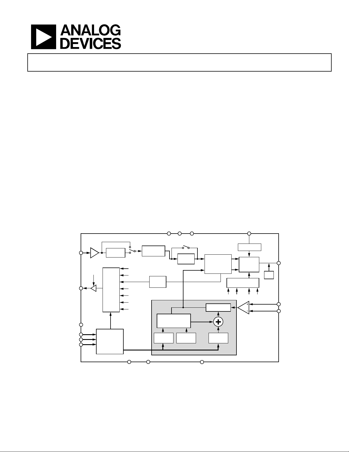
GENERAL DESCRIPTION
The ADF4157 is a 6 GHz fractional-N frequency synthesizer with
a 25-bit fixed modulus, allowing subhertz frequency resolution
at 6 GHz. It consists of a low noise digital phase frequency detector
(PFD), a precision charge pump, and a programmable reference
divider. There is a Σ-Δ based fractional interpolator to allow
programmable fractional-N division. The INT and FRAC values
define an overall N divider, N = INT + (FRAC/2
features cycle slip reduction circuitry, which leads to faster lock
times without the need for modifications to the loop filter.
Control of all on-chip registers is via a simple 3-wire interface.
The device operates with a power supply ranging from 2.7 V to
3.3 V and can be powered down when not in use.
25
). The ADF4157
FUNCTIONAL BLOCK DIAGRAM
Information furnished by Analog Devices is believed to be accurate and reliable. However, no
responsibility is assumed by Analog Devices for its use, nor for any infringements of patents or other
rights of third parties that may result from its use. Specifications subject to change without notice. No
license is granted by implication or otherwise under any patent or patent rights of Analog Devices.
Figure 1.
One Technology Way, P.O. Box 9106, Norwood, MA 02062-9106, U.S.A.
Tel: 781.329.4700
www.analog.com

ADF4157 Data Sheet
TABLE OF CONTENTS
Features .............................................................................................. 1
Applications ....................................................................................... 1
General Description ......................................................................... 1
Functional Block Diagram .............................................................. 1
Revision History ............................................................................... 2
Specifications ..................................................................................... 3
Timing Specifications .................................................................. 4
Absolute Maximum Ratings ............................................................ 5
Thermal Resistance ...................................................................... 5
ESD Caution .................................................................................. 5
Pin Configurations and Function Descriptions ........................... 6
Typical Performance Characteristics ............................................. 8
Circuit Description ........................................................................... 9
Reference Input Section ............................................................... 9
RF Input Stage ............................................................................... 9
RF INT Divider ............................................................................. 9
25-Bit Fixed Modulus .................................................................. 9
INT, FRAC, and R Relationship ................................................. 9
RF R Counter ................................................................................ 9
Phase Frequency Detector (PFD) and Charge Pump ............ 10
MUXOUT and Lock Detect ...................................................... 10
Input Shift Register..................................................................... 10
Program Modes .......................................................................... 10
Register Maps .................................................................................. 11
FRAC/INT Register (R0) Map.................................................. 12
LSB FRAC Register (R1) Map .................................................. 13
R Divider Register (R2) Map .................................................... 14
Function Register (R3) Map ..................................................... 16
Test Register (R4) Map .............................................................. 17
Applications Information .............................................................. 18
Initialization Sequence .............................................................. 18
RF Synthesizer: A Worked Example ........................................ 18
Reference Doubler and Reference Divider ............................. 18
Cycle Slip Reduction for Faster Lock Times ........................... 18
Fastlock Timer and Register Sequences .................................. 19
Fastlock: An Example ................................................................ 19
Fastlock: Loop Filter Topology ................................................. 19
Spur Mechanisms ....................................................................... 19
Low Frequency Applications .................................................... 20
Filter Design—ADIsimPLL....................................................... 20
Operating with Wide Loop Filter Bandwidths ....................... 20
PCB Design Guidelines for the Chip Scale Package .............. 20
Outline Dimensions ....................................................................... 21
Ordering Guide .......................................................................... 21
REVISION HISTORY
3/12—Rev. B to Rev. C
Changes to Table 1 ............................................................................ 3
Changes to Ordering Guide .......................................................... 21
9/11—Rev. A to Rev. B
Changes to Noise Characteristics Parameter ................................ 3
Changes to EPAD Note .................................................................... 6
1/09—Rev. 0 to Rev. A
Changes to Figure 1 .......................................................................... 1
Changes to Reference Characteristics Parameter, Table 1 .......... 3
Changes to Table 3 ............................................................................ 5
Changes to Figure 4 and Table 5 ..................................................... 6
Changes to Figure 15 ...................................................................... 10
Changes to Figure 16 ...................................................................... 11
Rev. C | Page 2 of 24
Changes to Figure 17 ...................................................................... 12
Changes to Figure 19 ...................................................................... 15
Added Negative Bleed Current Section, CLK Divider Mode
Section, and 12-Bit Clock Divider Value Section....................... 17
Changes to Reserved Bits Section and Figure 21 ....................... 17
Deleted Interfacing Section ........................................................... 18
Added Fastlock Timer and Register Sequences Section,
Fastlock: An Example Section, and Fastlock: Loop Filter
Topology Section ............................................................................ 19
Added Figure 22 and Figure 23; Renumbered Sequentially ..... 19
Added Operating with Wide Loop Filter Bandwidths
Section .............................................................................................. 20
Updated Outline Dimensions ....................................................... 21
7/07—Revision 0: Initial Ver s i on

Data Sheet ADF4157
Parameter
B Version1
Unit
Test Conditions/Comments
RF CHARACTERISTICS (3 V)
RF Input Frequency (RFIN)
0.5/6.0
GHz min/max
−10 dBm/0 dBm min/max; for lower frequencies, ensure slew rate
REFIN Input Sensitivity
0.4/AVDD
V p-p min/max
For 10 MHz < f
< 250 MHz, biased at AVDD/22
For 250 MHz < f
< 300 MHz, biased at AVDD/22
REFIN Input Capacitance
10
pF max
REFIN Input Current
±100
µA max
Phase Detector Frequency3
32
MHz max
CHARGE PUMP
ICP Sink/Source
Programmable
Low Value
312.5
µA typ
R
Range
2.7/10
kΩ min/max
ICP Three-State Leakage Current
1
nA typ
Sink and source current
ICP vs. VCP
2
% typ
0.5 V < VCP < VP – 0.5
ICP vs. Temperature
2
% typ
VCP = VP/2
LOGIC INPUTS
V
INL
, Input Low Voltage
0.6
V max
CIN, Input Capacitance
10
pF max
VOH, Output High Voltage
1.4
V min
Open-drain 1 kΩ pull-up to 1.8 V
VOL, Output Low Voltage
0.4
V max
IOL = 500 µA
AVDD
2.7/3.3
V min/max
VP
AVDD/5.5
V min/V max
IDD
29
mA max
23 mA typical
Normalized Phase Noise Floor
−211
dBc/Hz typ
PLL loop B/W = 500 kHz;
Normalized 1/f Noise (PN
)5
−110
dBc/Hz typ
10 kHz offset; normalized to 1 GHz
−133
dBc/Hz typ
@ 25 MHz PFD frequency
Phase Noise Performance7
@ VCO output
SPECIFICATIONS
AVDD = DVDD = 2.7 V to 3.3 V; VP = AVDD to 5.5 V; AGND = DGND = 0 V; TA = T
dBm referred to 50 Ω.
Table 1.
(SR) > 400 V/µs
REFERENCE CHARACTERISTICS
REFIN Input Frequency 10/300 MHz min/max For f
0.7/AVDD V p-p min/max
PHASE DETECTOR
to T
MIN
< 10 MHz, ensure slew rate > 50 V/µs
REFIN
, unless otherwise noted;
MAX
REFIN
REFIN
High Value 5 mA typ With R
Absolute Accuracy 2.5 % typ With R
SET
= 5.1 kΩ
SET
= 5.1 kΩ
SET
Matching 2 % typ 0.5 V < VCP < VP – 0.5
V
, Input High Voltage 1.4 V min
INH
I
, Input Current ±1 µA max
INH/IINL
LOGIC OUTPUTS
VOH, Output High Voltage VDD – 0.4 V min CMOS output chosen
POWER SUPPLIES
DVDD AVDD
Low Power Sleep Mode 10 µA typ
NOISE CHARACTERISTICS
(PN
SYNTH
4
)
1_f
measured at 100 kHz
Phase Noise Floor6 −137 dBc/Hz typ @ 10 MHz PFD frequency
5800 MHz Output8 −87 dBc/Hz typ @ 2 kHz offset, 25 MHz PFD frequency
1
Operating temperature of B version is −40°C to +85°C.
2
AC-coupling ensures AVDD/2 bias.
3
Guaranteed by design. Sample tested to ensure compliance.
4
The synthesizer phase noise floor is estimated by measuring the in-band phase noise at the output of the VCO and subtracting 20 log(N) (where N is the N divider
value) and 10 log(F
5
The PLL phase noise is composed of 1/f (flicker) noise plus the normalized PLL noise floor. The formula for calculating the 1/f noise contribution at an RF frequency, FRF,
and at a frequency offset f is given by PN = PN
6
The synthesizer phase noise floor is estimated by measuring the in-band phase noise at the output of the VCO and subtracting 20logN (where N is the N divider value).
7
The phase noise is measured with the EV-ADF4157SD1Z and the Agilent E5052A phase noise system.
8
f
= 100 MHz; f
REFIN
). PN
= PN
PFD
SYNTH
= 25 MHz; offset frequency = 2 kHz; RF
PFD
− 10 log(F
TOT
PFD
+ 10 log(10 kHz/f) + 20 log(FRF/1 GHz). Both the normalized phase noise floor and flicker noise are modeled in ADIsimPLL.
1_f
) − 20 log(N).
= 5800.25 MHz; N = 232; loop bandwidth = 20 kHz.
OUT
Rev. C | Page 3 of 24
ADF4157 Data Sheet
CLK
DATA
LE
LE
DB23 (MSB) DB22
DB2
(CONTROL BIT C3)
DB1
(CONTROL BIT C2)
DB0 (LSB)
(CONTROL BIT C1)
t
1
t
2
t
3
t
7
t
6
t
4
t
5
05874-002
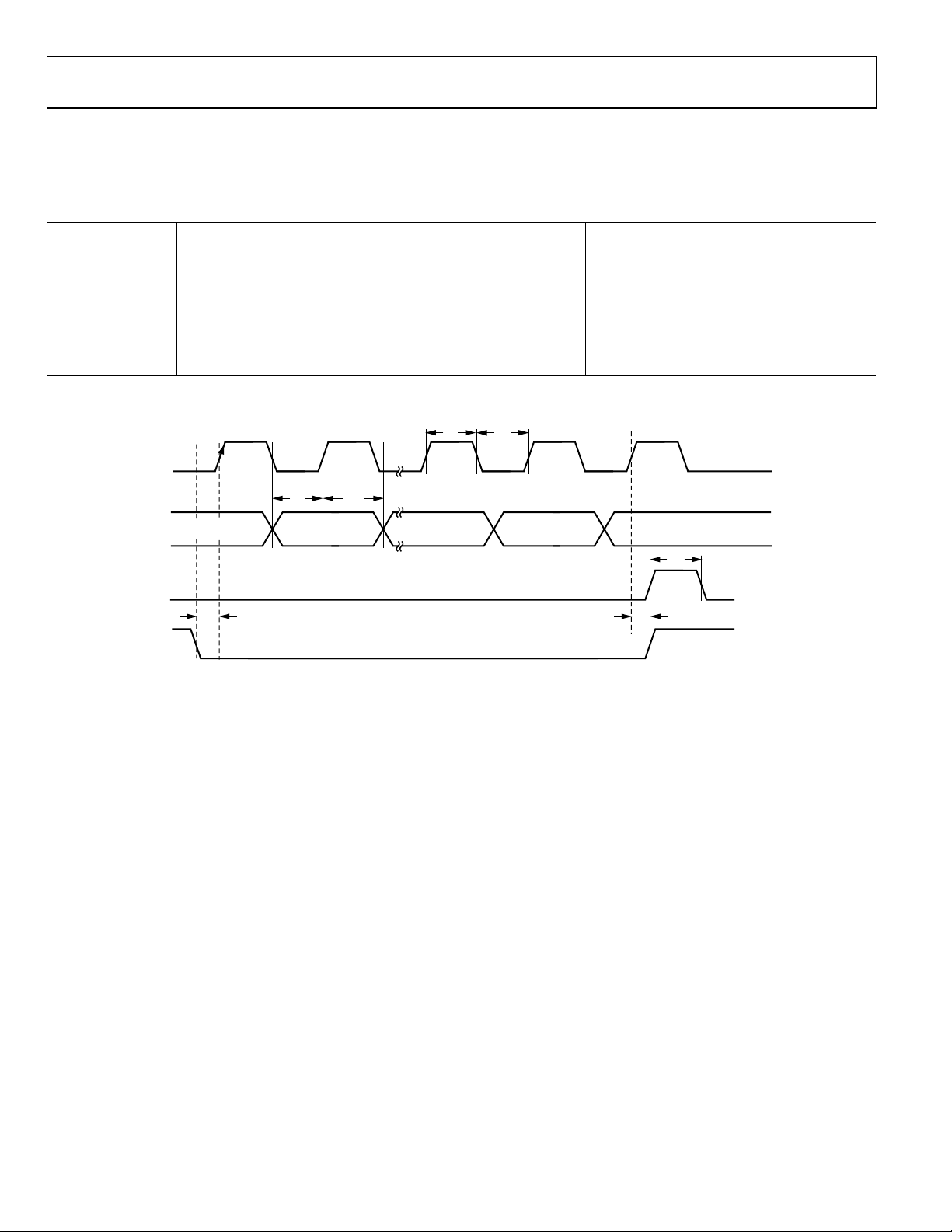
TIMING SPECIFICATIONS
AVDD = DVDD = 2.7 V to 3.3 V; VP = AVDD to 5.5 V; AGND = DGND = 0 V; TA = T
dBm referred to 50 Ω.
Table 2.
Parameter Limit at T
MIN
to T
(B Version) Unit Test Conditions/Comments
MAX
t1 20 ns min LE setup time
t2 10 ns min Data to clock setup time
t3 10 ns min Data to clock hold time
t4 25 ns min Clock high duration
t5 25 ns min Clock low duration
t6 10 ns min Clock to LE setup time
t7 20 ns min LE pulse width
MIN
to T
, unless otherwise noted;
MAX
Figure 2. Timing Diagram
Rev. C | Page 4 of 24
Data Sheet ADF4157
REFIN, RFINx to AGND/DGND
−0.3 V to VDD + 0.3 V
Package Type
θ
Unit
ABSOLUTE MAXIMUM RATINGS
TA = 25°C, GND = AGND = DGND = 0 V, VDD = AVDD = DVDD, unless otherwise noted.
Table 3.
Parameter Rating
AVDD/DVDD to AGND/DGND −0.3 V to +4 V
AVDD to DVDD −0.3 V to +0.3 V
VP to AGND/DGND −0.3 V to +5.8 V
VP to AVDD/DVDD −0.3 V to +5.8 V
Digital I/O Voltage to AGND/DGND −0.3 V to VDD + 0.3 V
Analog I/O Voltage to AGND/DGND −0.3 V to VDD + 0.3 V
Operating Temperature Range
Industrial (B Version) −40°C to +85°C
Storage Temperature Range −65°C to +125°C
Maximum Junction Temperature 150°C
Reflow Soldering
Peak Temperature 260°C
Time at Peak Temperature 40 sec
Stresses above those listed under Absolute Maximum Ratings
may cause permanent damage to the device. This is a stress
rating only; functional operation of the device at these or any
other conditions above those indicated in the operational
section of this specification is not implied. Exposure to absolute
maximum rating conditions for extended periods may affect
device reliability.
THERMAL RESISTANCE
θJA is specified for the worst-case conditions, that is, a device
soldered in a circuit board for surface-mount packages.
Table 4. Thermal Resistance
JA
TSSOP 112 °C/W
LFCSP (Paddle Soldered) 30.4 °C/W
ESD CAUTION
Rev. C | Page 5 of 24
ADF4157 Data Sheet
1
2
3
4
5
6
7
8
16
15
14
13
12
11
10
9
CP
CPGND
AGND
AV
DD
RF
IN
A
RF
IN
B
R
SET
DV
DD
MUXOUT
LE
CE
REF
IN
DGND
CLK
DATA
V
P
ADF4157
TOP VIEW
(Not to S cale)
05874-003
PIN 1
INDICATOR
1CPGND
2AGND
3AGND
4RF
IN
B
5RF
IN
A
13 DATA
14 LE
15 MUXOUT
NOTES
1. IT IS RECOMMENDED THAT THE EXPOSED PAD
BE THERMALLY CONNECTED TO A COPPE R
PLANE FO R E NHANCE D THERMAL PERF ORMANCE.
THIS PAD SHOULD BE CONNECT E D TO AGND.
12 CLK
11 CE
6AVDD7AVDD8REF
IN
10DGND
9DGND
18
V
P
19
R
SET
20
CP
17
DV
DD
16
DV
DD
TOP VIEW
(Not to S cale)
ADF4157
05874-004
7
6, 7
AVDD
Positive Power Supply for the RF Section. Decoupling capacitors to the digital ground plane
PIN CONFIGURATIONS AND FUNCTION DESCRIPTIONS
Figure 3. TSSOP Pin Configuration
Table 5. Pin Function Descriptions
TSSOP
Pin No.
1 19 R
LFCSP
Pin No. Mnemonic Description
Connecting a resistor between this pin and ground sets the maximum charge pump output
SET
current.
The relationship between I
5.25
I
CPMAX
=
R
SET
and R
CP
where:
R
= 5.1 kΩ.
SET
= 5 mA.
I
CPMAX
2 20 CP Charge Pump Output. When enabled, this pin provides ±ICP to the external loop filter, which, in
turn, drives the external VCO.
3 1 CPGND Charge Pump Ground. This is the ground return path for the charge pump.
4 2, 3 AGND Analog Ground. This is the ground return path of the prescaler.
5 4 RFINB Complementary Input to the RF Prescaler. This point should be decoupled to the ground plane
with a small bypass capacitor, typically 100 pF.
6 5 RFINA Input to the RF Prescaler. This small-signal input is normally ac-coupled from the VCO.
should be placed as close as possible to this pin. AVDD has a value of 3 V ± 10%. AVDD must have
the same voltage as DV
.
DD
8 8 REFIN Reference Input. This is a CMOS input with a nominal threshold of VDD/2 and an equivalent
input resistance of 100 kΩ. This input can be driven from a TTL or CMOS crystal oscillator, or it
can be ac-coupled.
9 9, 10 DGND Digital Ground.
10 11 CE Chip Enable. A logic low on this pin powers down the device and puts the charge pump output
into three-state mode.
11 12 CLK Serial Clock Input. This serial clock is used to clock in the serial data to the registers. The data is
12 13 DATA Serial Data Input. The serial data is loaded MSB first with the three LSBs being the control bits.
13 14 LE Load Enable, CMOS Input. When LE is high, the data stored in the input shift register is loaded
14 15 MUXOUT This multiplexer output allows the lock detect, the scaled RF, or the scaled reference frequency
latched into the input shift register on the CLK rising edge. This input is a high impedance
CMOS input.
This input is a high impedance CMOS input.
into one of the five latches, with the latch selected using the control bits.
to be accessed externally.
Rev. C | Page 6 of 24
SET
Figure 4. LFCSP Pin Configuration
is

Data Sheet ADF4157
TSSOP
Pin No.
15 16, 17 DVDD Positive Power Supply for the Digital Section. Decoupling capacitors to the digital ground
16 18 VP Charge Pump Power Supply. This should be greater than or equal to VDD. In systems where VDD
17 (EPAD) 21 (EPAD) Exposed Pad
LFCSP
Pin No. Mnemonic Description
plane should be placed as close as possible to this pin. DVDD has a value of 3 V ± 10%. DVDD
must have the same voltage as AV
is 3 V, it can be set to 5.5 V and used to drive a VCO with a tuning range of up to 5.5 V.
It is recommended that the exposed pad be thermally connected to a copper plane for
(EPAD)
enhanced thermal performance. The pad should be connected to AGND.
.
DD
Rev. C | Page 7 of 24
ADF4157 Data Sheet
10
–40
0 9
FREQUENCY ( GHz)
POWER (dBm)
5
0
–5
–10
–15
–20
–25
–30
–35
1 2 3 4 5 6 7 8
P = 4/5
P = 8/9
05874-016
0
–40
0 500
FREQUENCY (MHz)
POWER (dBm)
–5
–10
–15
–20
–25
–30
–35
100 200 300 400
V
DD
= 3V
05874-017
0
–160
1k 10M
FREQUENCY ( Hz )
PHASE NOISE (dBc/Hz)
–20
–40
–60
–80
–100
–120
–140
10k 100k 1M
RF = 5800.25MHz, P FD = 25MHz, N = 232,
FRAC = 335544, FREQUENCY RESOLUTION = 0.74Hz,
20kHz LOOP BW, I
CP
= 313µA, DSB INTEGRATED P HAS E
ERROR = 0.97° RM S , PHASE NOIS E @ 2kHz = –87dBc/Hz.
05874-018
6.00
5.65
–100 900
TIME (µs)
FREQUENCY ( GHz)
5.95
5.90
5.85
5.80
5.75
5.70
0 100 200 300 400 500 600 700 800
CSR OFF
CSR ON
05874-019
5.65
5.60
5.95
5.90
5.85
5.80
5.75
5.70
–100 900
TIME (µs)
FREQUENCY ( GHz)
0 100 200 300 400 500 600 700 800
CSR ON
CSR OFF
05874-020
6
–6
0 5.0
05874-021
VCP (V)
I
CP
(mA)
4
2
0
–2
–4
0.5 1.0 1.5 2.0 2.5 3.0 3.5 4.0 4.5
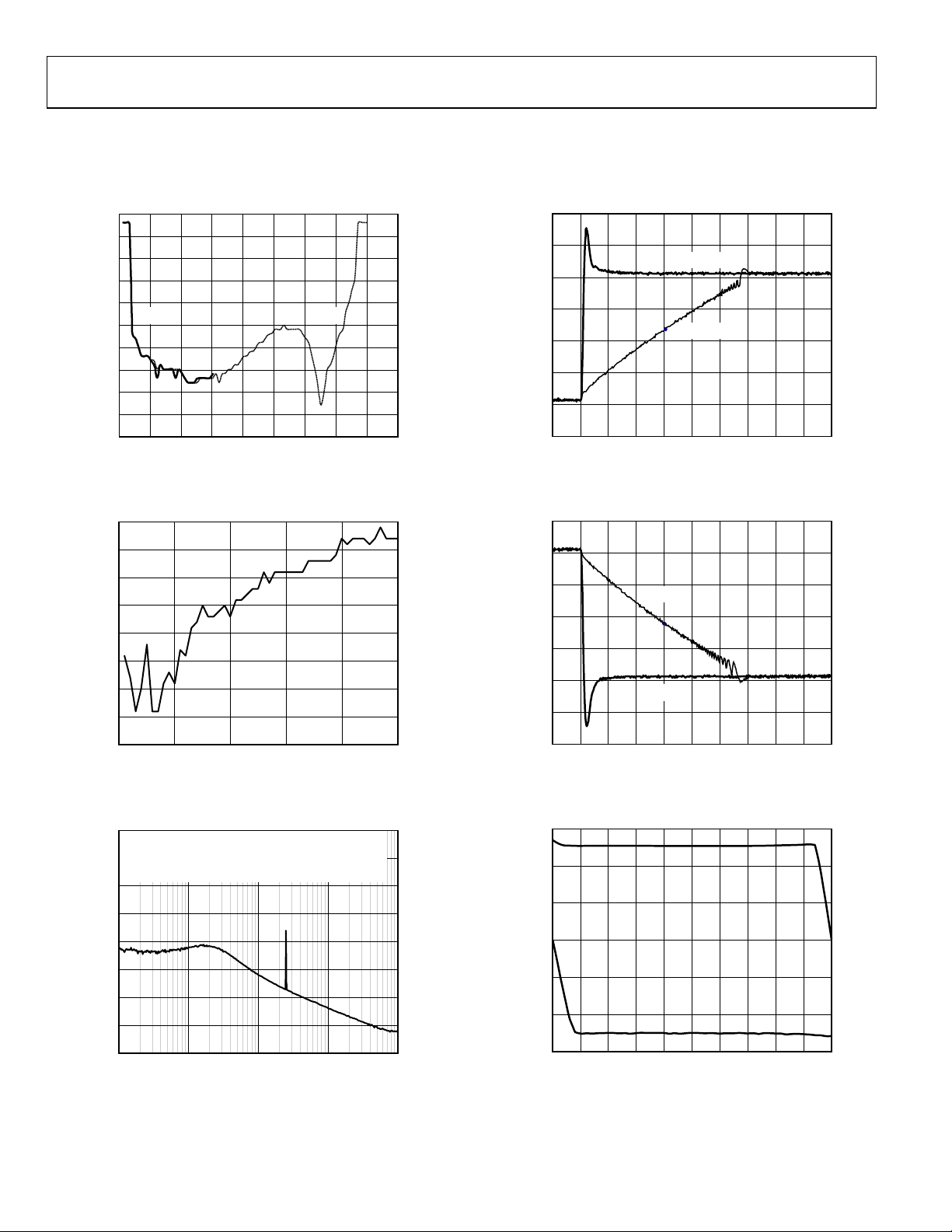
TYPICAL PERFORMANCE CHARACTERISTICS
PFD = 25 MHz, loop bandwidth = 20 kHz, reference = 100 MHz, ICP = 313 μA, phase noise measurements taken on the Agilent E5052A
phase noise system.
Figure 5. RF Input Sensitivity
Figure 6. Reference Input Sensitivity
Figure 8. Lock Time for 200 MHz Jump from 5705 MHz to 5905 MHz
with CSR On and Off
Figure 9. Lock Time for 200 MHz Jump from 5905 MHz to 5705 MHz
with CSR On and Off
(Note that the 250 kHz spur is an integer boundary spur; see the Spur
Figure 7. Phase Noise and Spurs
Mechanisms section for more information.)
Figure 10. Charge Pump Output Characteristics, Pump Up and Pump Down
Rev. C | Page 8 of 24

Data Sheet ADF4157
BUFFER
TO R COUNTE R
REF
IN
100kΩ
NC
SW2
SW3
NC
NC
SW1
POWER-DOWN
CONTROL
05874-005
BIAS
GENERATOR
1.6V
AGND
AV
DD
2kΩ 2kΩ
RF
IN
B
RF
IN
A
05874-006
THIRD-ORDER
FRACTIONAL
INTERPOLATOR
FRAC
VALUE
MOD
REG
INT
REG
RF N DIVIDE R
N = INT + FRAC/MOD
FROM RF
INPUT STAGE
TO PFD
N-COUNTER
05874-007
CIRCUIT DESCRIPTION
REFERENCE INPUT SECTION
The reference input stage is shown in Figure 11. SW1 and SW2
are normally closed switches. SW3 is normally open. When
power-down is initiated, SW3 is closed and SW1 and SW2 are
open. This ensures that there is no loading of the REF
pin on
IN
power-down.
Figure 11. Reference Input Stage
RF INPUT STAGE
The RF input stage is shown in Figure 12. It is followed by
a two-stage limiting amplifier to generate the current mode
logic (CML) clock levels needed for the prescaler.
INT, FRAC, AND R RELATIONSHIP
The INT and FRAC values, in conjunction with the R counter,
make it possible to generate output frequencies that are spaced
by fractions of the phase frequency detector (PFD). See the RF
Synthesizer: A Worked Example section for more information.
The RF VCO frequency (RF
= f
RF
OUT
× (INT + (FRAC/225)) (1)
PFD
) equation is
OUT
where:
RF
is the output frequency of the external voltage controlled
OUT
oscillator (VCO).
INT is the preset divide ratio of the binary 12-bit counter (23 to
4095).
FRAC is the numerator of the fractional division (0 to 2
= REFIN × [(1 + D)/(R × (1 + T))] (2)
f
PFD
25
− 1).
where:
REF
is the reference input frequency.
IN
D is the REF
doubler bit.
IN
R is the preset divide ratio of the binary 5-bit programmable
reference counter (1 to 32).
T is the REF
divide-by-2 bit (0 or 1).
IN
RF R COUNTER
The 5-bit RF R counter allows the input reference frequency
(REF
) to be divided down to produce the reference clock to
IN
the PFD. Division ratios from 1 to 32 are allowed.
Figure 12. RF Input Stage
RF INT DIVIDER
The RF INT counter allows a division ratio in the PLL feedback
counter. Division ratios from 23 to 4095 are allowed.
25-BIT FIXED MODULUS
The ADF4157 has a 25-bit fixed modulus. This allows output
frequencies to be spaced with a resolution of
f
= f
RES
where f
(PFD). For example, with a PFD frequency of 10 MHz,
frequency steps of 0.298 Hz are possible.
/225
PFD
is the frequency of the phase frequency detector
PFD
Figure 13. RF N Divider
Rev. C | Page 9 of 24

ADF4157 Data Sheet
U3
CLR2
Q2D2
U2
DOWN
UP
HI
HI
CP
–IN
+IN
CHARGE
PUMP
DELAY
CLR1
Q1D1
U1
05874-008
05874-009
ANALOG L OCK DETECT
MUXOUT
DV
DD
THREE-STATE OUTPUT
N DIVIDER O UTPUT
DV
DD
DGND
DGND
R DIVIDER O UTPUT
DIGITAL LOCK DETECT
SERIAL DAT A OUTPUT
CLK DIVIDE R OUTPUT
R DIVIDER/ 2
N DIVIDER/ 2
CONTROL
MUX
FASTLOCK SWITCH
Control Bits
PHASE FREQUENCY DETECTOR (PFD) AND CHARGE PUMP
The PFD takes inputs from the R counter and the N counter
and produces an output proportional to the phase and frequency difference between them. Figure 14 is a simplified
schematic of the phase frequency detector. The PFD includes
a fixed delay element that sets the width of the antibacklash
pulse, which is typically 3 ns. This pulse ensures that there is no
dead zone in the PFD transfer function and gives a consistent
reference spur level.
Figure 14. PFD Simplified Schematic
MUXOUT AND LOCK DETECT
The output multiplexer on the ADF4157 allows the user to access
various internal points on the chip. The state of MUXOUT is
controlled by M4, M3, M2, and M1 (see Figure 17). Figure 15
shows the MUXOUT section in block diagram form.
INPUT SHIFT REGISTER
The ADF4157 digital section includes a 5-bit RF R counter, a
12-bit RF N counter, and a 25-bit FRAC counter. Data is clocked
into the 32-bit input shift register on each rising edge of CLK.
The data is clocked in MSB first. Data is transferred from the
input shift register to one of five latches on the rising edge of
LE. The destination latch is determined by the state of the three
control bits (C3, C2, and C1) in the input shift register. The s e
are the three LSBs, DB2, DB1, and DB0, as shown in Figure 2.
The truth table for these bits is shown in Table 6. Figure 16
shows a summary of how the latches are programmed.
PROGRAM MODES
Table 6 and Figure 16 through Figure 21 show how to set up
the program modes in the ADF4157.
Several settings in the ADF4157 are double-buffered. These
include the LSB FRAC value, R counter value, reference doubler,
and current setting. This means that two events have to occur
before the part uses a new value of any of the double-buffered
settings. First, the new value is latched into the device by writing to
the appropriate register. Second, a new write must be performed
on Register 0, R0.
For example, updating the fractional value can involve a write
to the 13 LSB bits in R1 and the 12 MSB bits in R0. R1 should
be written to first, followed by the write to R0. The frequency
change begins after the write to R0. Double buffering ensures
that the bits written to in R1 do not take effect until after the
write to R0.
Figure 15. MUXOUT Schematic
Table 6. C3, C2, and C1 Truth Table
C3 C2 C1 Register
0 0 0 Register 0 (R0)
0 0 1 Register 1 (R1)
0 1 0 Register 2 (R2)
0 1 1 Register 3 (R3)
1 0 0 Register 4 (R4)
Rev. C | Page 10 of 24

Data Sheet ADF4157
DB31
CONTROL
BITS
12-BIT MSB FRACTIONAL V ALUE
(FRAC)
12-BIT INTEGER VALUE ( INT)
MUXOUT
CONTROL
DB30 DB29 DB28 DB27 DB26 DB25 DB24 DB23 DB22 DB21 DB20 DB19 DB18 DB17 DB16 DB15 DB14 DB13 DB12 DB11 DB10 DB9 DB8 DB7 DB6 DB5 DB4 DB3 DB2 DB1 DB0
0 M4 M3 M2 M1 N12 N11 N10 N9 N8 N7 N6 N5 N4 N3 N2 N1 F25 F24 F23 F22 F21 F20 F19 F18 F17 F16 F15 F14 C3(0) C2(0) C1(0)
RESERVED
FRAC/INT REGISTER (R0)
DB31
CONTROL
BITS
RESERVED
13-BIT LS B FRACTIONAL V ALUE
(FRAC) (DBB)
RESERVED
RESERVED RESERVED
RESERVED
DB30 DB29 DB28 DB27 DB26 DB25 DB24 DB23 DB22 DB21 DB20 DB19 DB18 DB17 DB16 DB15 DB14 DB13 DB12 DB11 DB10 DB9 DB8 DB7 DB6 DB5 DB4 DB3 DB2 DB1 DB0
0 0 0 0 F13 F12 F11 F10 F9 F8 F7 F6 F5 F4 F3 F2 F1 0 0 0 0 0 0 0 0 0 0 0 0 C3(0) C2(0) C1(1)
LSB FRAC REGISTER (R1)
DB31
RESERVED
PD
PD
POLARITY
LDP
COUNTER
RESET
CP
THREE-STATE
CONTROL
BITS
DB30 DB29 DB28 DB27 DB26 DB25 DB24 DB23 DB22 DB21 DB20 DB19 DB18 DB17 DB16 DB15 DB14 DB13 DB12 DB11 DB10 DB9 DB8 DB7 DB6 DB5 DB4 DB3 DB2 DB1 DB0
0 0 0 0 0 0 0 0 0 0 0 0 0 0 0 0 0 U12 0 0 0 0 0 0 U11 U10 U9 U8 U7 C3(0) C2(1) C1(1)
FUNCTION REGISTER (R3)
DB31
12-BIT CLOCK DIVIDER VALUE
CONTROL
BITS
DB30 DB29 DB28 DB27 DB26 DB25 DB24 DB23 DB22 DB21 DB20 DB19 DB18 DB17 DB16 DB15 DB14 DB13 DB12 DB11 DB10 DB9 DB8 DB7 DB6 DB5 DB4 DB3 DB2 DB1 DB0
0 0 0 0 0 0 0 NB2 NB1 0 0 C2 C1 D12 D11 D10 D9 D8 D7 D6 D5 D4 D3 D2 D1 C3(1) C2(0) C1(0)
TEST REGI STER (R4)
NOTES
1. DBB = DOUBLE BUFFERED BIT(S).
DB31
RESERVED5-BIT R COUNTER
RESERVED
RESERVED
CSR EN
RESERVED
PRESCALER
RDIV2 DBB
CURRENT
SETTING
REFERENCE
DOUBLER DBB
CONTROL
BITS
DB30 DB29 DB28 DB27 DB26 DB25 DB24 DB23 DB22 DB21 DB20 DB19 DB18 DB17 DB16 DB15 DB14 DB13 DB12 DB11 DB10 DB9 DB8 DB7 DB6 DB5 DB4 DB3 DB2 DB1 DB0
0 0 0 C1 CPI4 CPI3 CPI2 CPI1 0 P1 U2 U1 R5 R4 R3 R2 R1 0 0 0 0 0 0 0 0 0 0 0 0 C3(0) C2(1) C1(0)
R DIVIDER REGISTER (R2)
DBB DBB
05874-010
SD
RESET
RESERVED
CLK
DIV
MODE
NEG
BLEED
CURRENT
0
0
0 0
REGISTER MAPS
Figure 16. Register Summary
Rev. C | Page 11 of 24

ADF4157 Data Sheet
05874-011
FRAC/INT REGISTER (R0) MAP
With R0[2:0] set to 000, the on-chip FRAC/INT register is
programmed as shown in Figure 17.
Reserved Bit
The reserved bit should be set to 0 for normal operation.
MUXOUT
The on-chip multiplexer is controlled by Bits DB[30:27] on the
ADF4157. See Figure 17 for the truth table.
12-Bit INT Value
These 12 bits control what is loaded as the INT value. This is
used to determine the overall feedback division factor. It is used
in Equation 1. See the INT, FRAC, and R Relationship section
for more information.
12-Bit MSB FRAC Value
These 12 bits, along with Bits DB[27:15] in the LSB FRAC
register (R1), control what is loaded as the FRAC value into
the fractional interpolator. This is part of what determines the
overall feedback division factor. It is also used in Equation 1.
These 12 bits are the most significant bits (MSB) of the 25-bit
FRAC value, and Bits DB[27:15] in the LSB FRAC register (R1)
are the least significant bits (LSB). See the RF Synthesizer: A
Worked Example section for more information.
MUXOUT
CONTROL
RESERVED
DB31
DB30 DB29 DB28 DB27 DB26 DB25 DB24 DB23 DB22 DB21 DB20 DB19 DB18 DB17 DB16 DB15 DB14 DB13 DB12 DB11 DB10 DB9 DB8 DB7 DB6 DB5 DB4 DB3 DB2 DB1 DB0
0 M4 M3 M2 M1 N12 N11 N10 N9 N8 N7 N6 N5 N4 N3 N2 N1 F25 F24 F23 F22 F21 F20 F19 F18 F17 F16 F15 F14 C3(0) C2(0) C1(0)
M4 M3 M2 M1 OUTPUT
0 0 0 0 THREE-STATE OUTPUT
0 0 0 1 DV
0 0 1 0 DGND
0 0 1 1 R DIVIDER OUTPUT
0 1 0 0 N DIVIDER OUTPUT
0 1 0 1 ANALOG LOCK DETECT
0 1 1 0 DIGITAL LOCK DETECT
0 1 1 1 SERIAL DATA OUTPUT
1 0 0 0 RESERVED
1 0 0 1 RESERVED
1 0 1 0 CLK DIVIDER OUTPUT
1 0 1 1 RESERVED
1 1 0 0 FASTLOCK SWITCH
1 1 0 1 R DIVIDER/2
1 1 1 0 N DIVIDER/2
1 1 1 1 RESERVED
12-BIT INTEGER VALUE ( INT)
DD
N12 N11 N10 N9 N8 N7 N6 N5 N4 N3 N2 N1
0 0 0 0 0 0 0 1 0 1 1 1 23
0 0 0 0 0 0 0 1 1 0 0 0 24
0 0 0 0 0 0 0 1 1 0 0 1 25
0 0 0 0 0 0 0 1 1 0 1 0 26
. . . . . . . . . . . . .
. . . . . . . . . . . . .
. . . . . . . . . . . . .
1 1 1 1 1 1 1 1 1 1 0 1 4093
1 1 1 1 1 1 1 1 1 1 1 0 4094
1 1 1 1 1 1 1 1 1 1 1 1 4095
12-BIT MSB FRACTIONAL V ALUE
F12 F11 .......... F2 F1
0 0 .......... 0 0 0
0 0 .......... 0 1 1
0 0 .......... 1 0 2
0 0 .......... 1 1 3
. . .......... . . .
. . .......... . . .
. . .......... . . .
1 1 .......... 0 0 4092
1 1 .......... 0 1 4093
1 1 .......... 1 0 4094
1 1 .......... 1 1 4095
*THE FRAC VAL UE IS MADE UP OF THE 12-BIT M S B S TORED IN
REGIST E R 0, AND THE 13-BIT LSB REGIS TER STORED IN
REGIST E R 1. FRAC VALUE = 13- BIT LSB + 12- BIT MSB × 2
(FRAC)
INTEGERVALUE
(INT)
MSB FRACTI ONAL VALUE
(FRAC)*
CONTROL
BITS
13
.
Figure 17. FRAC/INT Register (R0) Map
Rev. C | Page 12 of 24

Data Sheet ADF4157
DB31
CONTROL
BITS
RESERVED
13-BIT LS B FRACTIONAL V ALUE
(FRAC) (DBB)
RESERVED
DB30 DB29 DB28 DB27 DB26 DB25 DB24 DB23 DB22 DB21 DB20 DB19 DB18 DB17 DB16 DB15 DB14 DB13 DB12 DB11 DB10 DB9 DB8 DB7 DB6 DB5 DB4 DB3 DB2 DB1 DB0
0 0 0 0 F13 F12 F11 F10 F9 F8 F7 F6 F5 F4 F3 F2 F1 0 0 0 0 0 0 0 0 0 0 0 0 C3(0) C2(0) C1(1)
F25 F24 .......... F14 F13
LSB FRACTIONAL VALUE
(FRAC)*
0 0 .......... 0 0 0
0 0 .......... 0 1 1
0 0 .......... 1 0 2
0 0 .......... 1 1 3
. . .......... . . .
. . .......... . . .
. . .......... . . .
1 1 .......... 0 0 8188
1 1 .......... 0 1 8189
1 1 .......... 1 0 8190
1 1 .......... 1 1 8191
*THE FRAC VAL UE IS MADE UP OF THE 12-BIT M S B S TORED IN
REGIST E R 0, AND THE 13-BIT LSB REGIS TER STORED IN
REGIST E R 1. FRAC VALUE = 13- BIT LSB + 12- BIT MSB × 2
13
.
05874-012
LSB FRAC REGISTER (R1) MAP
With R1[2:0] set to 001, the on-chip LSB FRAC register is
programmed as shown in Figure 18.
13-Bit LSB FRAC Value
These 13 bits, along with Bits DB[14:3] in the INT/FRAC
register (R0), control what is loaded as the FRAC value into
the fractional interpolator. This is part of what determines
the overall feedback division factor. It is also used in Equation 1.
These 13 bits are the least significant bits of the 25-bit FRAC
value, and Bits DB[14:3] in the INT/FRAC register are the most
significant bits. See the RF Synthesizer: A Worked Example
section for more information.
Reserved Bits
All reserved bits should be set to 0 for normal operation.
Figure 18. LSB FRAC Register (R1) Map
Rev. C | Page 13 of 24

ADF4157 Data Sheet
R DIVIDER REGISTER (R2) MAP
With R2[2:0] set to 010, the on-chip R divider register is
programmed as shown in Figure 19.
CSR Enable
Setting this bit to 1 enables cycle slip reduction. This is a
method for improving lock times. Note that the signal at the PFD
must have a 50% duty cycle for cycle slip reduction to work. In
addition, the charge pump current setting must be set to a
minimum. See the Cycle Slip Reduction for Faster Lock Times
section for more information.
Note also that the cycle slip reduction feature can only be
operated when the phase detector polarity setting is positive
(DB6 in Register 3). It cannot be used if the phase detector
polarity is set to negative.
Charge Pump Current Setting
Bits DB[27:24] set the charge pump current setting. This should
be set to the charge pump current that the loop filter is designed
with (see Figure 19).
Prescaler (P/P + 1)
The dual-modulus prescaler (P/P + 1), along with INT, FRAC,
and MOD, determine the overall division ratio from RF
the PFD input.
Operating at CML levels, it takes the clock from the RF input
stage and divides it down for the counters. It is based on
a synchronous 4/5 core. When set to 4/5, the maximum RF
frequency allowed is 3 GHz. Therefore, when operating
the ADF4157 above 3 GHz, the prescaler must be set to 8/9.
The prescaler limits the INT value.
With P = 4/5, N
With P = 8/9, N
MIN
MIN
= 23.
= 75.
IN
x to
RDIV2
Setting this bit to 1 inserts a divide-by-2 toggle flip-flop
between the R counter and the PFD. This can be used to
provide a 50% duty cycle signal at the PFD for use with cycle
slip reduction.
Reference Doubler
Setting DB[20] to 0 feeds the REFIN signal directly to the 5-bit
RF R counter, disabling the doubler. Setting this bit to 1 multiplies
the REF
R counter. When the doubler is disabled, the REF
frequency by a factor of 2 before feeding into the 5-bit
IN
falling edge
IN
is the active edge at the PFD input to the fractional synthesizer.
When the doubler is enabled, both the rising edge and falling
edge of REF
The maximum allowed REF
become active edges at the PFD input.
IN
frequency when the doubler is
IN
enabled is 30 MHz.
5-Bit R Counter
The 5-bit R counter allows the input reference frequency
(REF
) to be divided down to produce the reference clock to
IN
the phase frequency detector (PFD). Division ratios from
1 to 32 are allowed.
Reserved Bits
All reserved bits should be set to 0 for normal operation.
Rev. C | Page 14 of 24

Data Sheet ADF4157
DB31
RESERVED5-BIT R CO UNTER
RESERVED
RESERVED
CSR EN
RESERVED
PRESCALER
CURRENT
SETTING
CONTROL
BITS
DB30 DB29 DB28 DB27 DB26 DB25 DB24 DB23 DB22 DB21 DB20 DB19 DB18 DB17 DB16 DB15 DB14 DB13 DB12 DB11 DB10 DB9 DB8 DB7 DB6 DB5 DB4 DB3 DB2 DB1 DB0
0 0 0 C1 CPI4 CPI3 CPI2 CPI1 0 P1 U2 U1 R5 R4 R3 R2 R1 0 0 0 0 0 0 0 0 0 0 0 0 C3(0) C2(1) C1(0)
C1
CYCLE SLIP
REDUCTION
0 DISABLED
1 ENABLED
U1
REFERENCE
DOUBLER
0 DISABLED
1 ENABLED
R5 R4 R3 R2 R1 R COUNTER DIVIDE RATIO
0 0 0 0 1 1
0 0 0 1 0 2
0 0 0 1 1 3
0 0 1 0 0 4
. . . . .
. . . . .
. . . . .
1 1 1 0 1 29
1 1 1 1 . 30
1 1 1 1 1 31
0 0 0 0 0 32
U2 R DIVIDER
0 DISABLED
1 ENABLED
P1 PRESCALER
0 4/5
1 8/9
ICP(mA)
CPI4 CPI3 CPI2 CPI1 5.1kΩ
0 0 0 0 0.31
0 0 0 1 0.63
0 0 1 0 0.94
0 0 1 1 1.25
0 1 0 0 1.57
0 1 0 1 1.88
0 1 1 0 2.19
0 1 1 1 2.5
1 0 0 0 2.81
1 0 0 1 3.13
1 0 1 0 3.44
1 0 1 1 3.75
1 1 0 0 4.06
1 1 0 1 4.38
1 1 1 0 4.69
1 1 1 1 5
05874-013
DBB DBB
RDIV2 DBB
REFERENCE
DOUBLER DBB
Figure 19. R Divider Register (R2) Map
Rev. C | Page 15 of 24

ADF4157 Data Sheet
DB31
RESERVED
PD
PD
POLARITY
LDP
COUNTER
RESET
CP
THREE-STATE
CONTROL
BITS
DB30 DB29 DB28 DB27 DB26 DB25 DB24 DB23 DB22 DB21 DB20 DB19 DB18 DB17 DB16 DB15 DB14 DB13 DB12 DB11 DB10 DB9 DB8 DB7 DB6 DB5 DB4 DB3 DB2 DB1 DB0
0 0 0 0 0 0 0 0 0 0
0 0 0 0 0 0 0 U12 0 0 0 0 0 0 U11 U10 U9 U8 U7 C3(0) C2(1) C1(1)
U9 POWER-DOWN
0 DISABLED
1 ENABLED
U11
LDP
0 24 PFD CYCLES
1 40 PFD CYCLES
U7
COUNTER
RESET
0 DISABLED
1 ENABLED
U10 PD POLARITY
0 NEGATIVE
1 POSITIVE
U8CPTHREE-STATE
0 DISABLED
1 ENABLE
D
05874-014
SD
RESET
RESERVED
U12 SD RESET
0 ENABLED
1 DISABLED
FUNCTION REGISTER (R3) MAP
With R3[2:0] set to 011, the on-chip function register is
programmed as shown in Figure 20.
Reserved Bits
All reserved bits should be set to 0 for normal operation.
Σ-Δ Reset
For most applications, DB14 should be set to 0. When DB14 is
set to 0, the Σ-Δ modulator is reset on each write to Register 0.
If it is not required that the Σ-Δ modulator be reset on each
Register 0 write, this bit should be set to 1.
Lock Detect Precision (LDP)
When DB[7] is programmed to 0, 24 consecutive PFD cycles of
15 ns must occur before digital lock detect is set. When this bit
is programmed to 1, 40 consecutive reference cycles of 15 ns
must occur before digital lock detect is set.
Phase Detector Polarity
DB[6] sets the phase detector polarity. When the VCO
characteristics are positive, this should be set to 1. When they
are negative, it should be set to 0.
RF Power-Down
DB[5] provides the programmable power-down mode. Setting
this bit to 1 performs a power-down. Setting this bit to 0 returns
the synthesizer to normal operation. While in software powerdown mode, the part retains all information in its registers.
Only when supplies are removed are the register contents lost.
When a power-down is activated, the following events occur:
• All active dc current paths are removed.
• The synthesizer counters are forced to their load state
conditions.
• The charge pump is forced into three-state mode.
• The digital lock detect circuitry is reset.
• The RF
x input is debiased.
IN
• The input shift register remains active and capable of
loading and latching data.
RF Charge Pump Three-State
DB[4] puts the charge pump into three-state mode when
programmed to 1. It should be set to 0 for normal operation.
RF Counter Reset
DB[3] is the RF counter reset bit for the ADF4157. When this
is 1, the RF synthesizer counters are held in reset. For normal
operation, this bit should be 0.
Figure 20. Function Register (R3) Map
Rev. C | Page 16 of 24

Data Sheet ADF4157
DB31
12-BIT CLOCK DIVIDER VALUERESERVED RESERVED
RESERVED
CONTROL
BITS
DB30 DB29 DB28 DB27 DB26 DB25 DB24 DB23 DB22 DB21 DB20 DB19 DB18 DB17 DB16 DB15 DB14 DB13 DB12 DB11 DB10 DB9 DB8 DB7 DB6 DB5 DB4 DB3 DB2 DB1 DB0
0 0 0 0 0 0 0 NB2 NB1 0 0 C2 C1 D12
D11 D10 D9 D8 D7 D6 D5 D4 D3 D2 D1 C3(1) C2(0) C1(0)
05874-015
NB2 NB1 NEGAT IVE BLEED CURRE NT
0 0 OFF
1 1 ON
D12 D11 .......... D2 D1 CLOCK DIVIDE R V ALUE
0 0 .......... 0 0 0
0 0 .......... 0 1 1
0 0 .......... 1 0 2
0 0 .......... 1 1 3
. . .......... . . .
. . .......... . . .
. . .......... . . .
1 1 .......... 0 0 4092
1
1 .......... 0 1 4093
1 1 .......... 1 0 4094
1 1 .......... 1 1 4095
C2 C1 CLOCK DI V IDER MODE
0 0
CLOCK DIVIDER OFF
0 1 S WITCHED R FAS TLOCK ENABL E
0 0
0
0
NEG
BLEED
CURR-
ENT
CLK
DIV
MODE
TEST REGISTER (R4) MAP
With R4[2:0] set to 100, the on-chip test register (R4) is
programmed as shown in Figure 21.
Negative Bleed Current
Setting Bits DB[24:23] to 11 turns on the constant negative
bleed current. This ensures that the charge pump operates out
of the dead zone. Thus the phase noise is not degraded and the
level of spurs is lower. Enabling constant negative bleed current
is particularly important on channels close to multiple PFD
frequencies.
CLK Divider Mode
Setting Bits DB[20:19] to 01 enables switched R fastlock.
12-Bit Clock Divider Value
Bits DB[18:7] are used to program the clock divider, which
determines for how long the loop remains in wideband mode
while the switched R fastlock technique is used.
Reserved Bits
All reserved bits should be set to 0 for normal operation.
Figure 21. Test Register (R4) Map
Rev. C | Page 17 of 24

ADF4157 Data Sheet
APPLICATIONS INFORMATION
INITIALIZATION SEQUENCE
After powering up the part, this programming sequence must
be followed:
1. Te st register (R4)
2. Function register (R3)
3. R divider register (R2)
4. LSB FRAC register (R1)
5. FRAC/INT register (R0)
RF SYNTHESIZER: A WORKED EXAMPLE
The following equation governs how the synthesizer should be
programmed:
RF
= [N + (FRAC/225)] × [f
OUT
] (3)
PFD
where:
RF
is the RF frequency output.
OUT
N is the integer division factor.
FRAC is the fractionality.
f
= REFIN × [(1 + D)/(R × (1 + T))] (4)
PFD
where:
REF
is the reference frequency input.
IN
D is the RF REF
doubler bit.
IN
R is the RF reference division factor.
T is the reference divide-by-2 bit (0 or 1).
For example, in a system where a 5.8002 GHz RF frequency
output (RF
input (REF
f
RES
f
RES
) is required and a 10 MHz reference frequency
OUT
) is available, the frequency resolution is
IN
= REFIN/225
= 10 MHz/225 = 0.298 Hz
From Equation 4,
f
= [10 MHz × (1 + 0)/1] = 10 MHz
PFD
5.8002 GHz = 10 MHz × (N + FRAC/2
25
)
Calculating N and FRAC values,
N = int(RF
FRAC = F
F
= int(((RF
MSB
F
= int(((((RF
LSB
OUT/fPFD
× 213 + F
MSB
) = 580
LSB
) − N) × 212) = 81
OUT/fPFD
) − N) × 212) − F
OUT/fPFD
) × 213) = 7537
MSB
where:
F
is the 12-bit MSB FRAC value in Register R0.
MSB
F
is the 13-bit LSB FRAC value in Register R1.
LSB
int() makes an integer of the argument in brackets.
REFERENCE DOUBLER AND REFERENCE DIVIDER
The on-chip reference doubler allows the input reference signal
to be doubled. This is useful for increasing the PFD comparison
frequency. Making the PFD frequency higher improves the noise
performance of the system. Doubling the PFD frequency
usually improves noise performance by 3 dB. It is important to
note that the PFD cannot be operated above 32 MHz due to
a limitation in the speed of the Σ-Δ circuit of the N divider.
CYCLE SLIP REDUCTION FOR FASTER LOCK TIMES
In fastlocking applications, a wide loop filter bandwidth is
required for fast frequency acquisition, resulting in increased
integrated phase noise and reduced spur attenuation. Using
cycle slip reduction, the loop bandwidth can be kept narrow to
reduce integrated phase noise and attenuate spurs while still
realizing fast lock times.
Cycle Slips
Cycle slips occur in integer-N/fractional-N synthesizers when
the loop bandwidth is narrow compared to the PFD frequency.
The phase error at the PFD inputs accumulates too fast for the PLL
to correct, and the charge pump temporarily pumps in the wrong
direction, slowing down the lock time dramatically. The ADF4157
contains a cycle slip reduction circuit to extend the linear range
of the PFD, allowing faster lock times without loop filter changes.
When the ADF4157 detects that a cycle slip is about to occur, it
turns on an extra charge pump current cell. This outputs a constant
current to the loop filter or removes a constant current from the
loop filter (depending on whether the VCO tuning voltage needs
to increase or decrease to acquire the new frequency). The effect is
that the linear range of the PFD is increased. Stability is maintained because the current is constant and is not a pulsed current.
If the phase error increases again to a point where another cycle
slip is likely, the ADF4157 turns on another charge pump cell.
This continues until the ADF4157 detects that the VCO frequency
has exceeded the desired frequency. It then begins to turn off
the extra charge pump cells one by one until they are all turned
off and the frequency is settled.
Up to seven extra charge pump cells can be turned on. In most
applications, it is enough to eliminate cycle slips altogether,
giving much faster lock times.
Setting Bit DB28 in the R Divider register (R2) to 1 enables cycle
slip reduction. Note that a 45% to 55% duty cycle is needed on
the signal at the PFD for CSR to operate correctly. The reference
divide-by-2 flip-flop can help to provide a 50% duty cycle at the
PFD. For example, if a 100 MHz reference frequency is available,
and the user wants to run the PFD at 10 MHz, setting the R divide
factor to 10 results in a 10 MHz PFD signal that is not 50% duty
cycle. By setting the R divide factor to 5 and enabling the reference
divide-by-2 bit, a 50% duty cycle 10 MHz signal can be achieved.
Note that the cycle slip reduction feature can only be operated
when the phase detector polarity setting is positive (DB6 in
Register 3). It cannot be used if the phase detector polarity is
set to negative.
Rev. C | Page 18 of 24

ADF4157
CP
MUXOUT
C1
C2
R2
R1
R1A
C3
VCO
05874-022
ADF4157
CP
MUXOUT
C1 C2
R2
R1R1A
C3
VCO
05874-023
Data Sheet ADF4157
FASTLOCK TIMER AND REGISTER SEQUENCES
If the fastlock mode is used, a timer value needs to be loaded into
the PLL to determine the time spent in wide bandwidth mode.
When Bits DB[20:19] in Register 4 (R4) are set to 01 (switched
R fastlock enable), the timer value is loaded via the 12-bit clock
divider value. To use fastlock, the PLL must be written to in the
following sequence:
1. Us e the initialization sequence (see the Initialization
Sequence section) only once after powering up the part.
2. Load Register 4 (R4) with Bits DB[20:19] set to 01 and the
chosen fastlock timer value (DB18 to DB7). Note that the
duration that the PLL remains in wide bandwidth is equal
to the fastlock timer/f
PFD
.
FASTLOCK: AN EXAMPLE
If a PLL has f
the PLL is set to wide bandwidth for 40 µs.
If the time period set for the wide bandwidth is 40 µs, then
Fastlock Timer Value = Time in Wide Bandwidth × f
Fastlock Timer Value = 40 µs × 13 MHz = 520
Therefore, 520 must be loaded into the clock divider value in
Register 4 (R4) in Step 2 of the sequence described in the
Fastlock Timer and Register Sequences section.
= 13 MHz and a required lock time of 50 µs,
PFD
FASTLOCK: LOOP FILTER TOPOLOGY
To us e f a st -lock mode, an extra connection from the PLL to the
loop filter is needed. The damping resistor in the loop filter must
be reduced to ¼ of its value while in wide bandwidth mode. This is
required because the charge pump current is increased by 16
while in wide bandwidth mode, and stability must be ensured.
During fastlock, the MUXOUT pin (after setting MUXOUT to
fastlock switch by setting Bits DB[30:27] in Register 0 to 1100) is
shorted to ground (this is accomplished by settings Bits DB[20:19]
in Register 4 to 01—switched R fastlock enable). The following
two topologies can be used:
• Divide the damping resistor (R1) into two values (R1 and
R1A) that have a ratio of 1:3 (see Figure 22).
• Connect an extra resistor (R1A) directly from MUXOUT,
as shown in Figure 23. The extra resistor must be chosen
such that the parallel combination of an extra resistor and
the damping resistor (R1) is reduced to ¼ of the original
value of R1 (see Figure 23).
Figure 22. Fast-Lock Loop Filter Topology—Topology 1
PFD
Rev. C | Page 19 of 24
Figure 23. Fastlock Loop Filter Topology—Topology 2
SPUR MECHANISMS
The fractional interpolator in the ADF4157 is a third-order Σ-Δ
modulator (SDM) with a 25-bit fixed modulus (MOD). The
SDM is clocked at the PFD reference rate (f
output frequencies to be synthesized at a channel step resolution of
f
/MOD. The various spur mechanisms possible with fractional-
PFD
N synthesizers, and how they affect the ADF4157, are discussed in
this section.
Fractional Spurs
In most fractional synthesizers, fractional spurs can appear at
the set channel spacing of the synthesizer. In the ADF4157,
these spurs do not appear. The high value of the fixed modulus
in the ADF4157 makes the Σ-Δ modulator quantization error
spectrum look like broadband noise, effectively spreading the
fractional spurs into noise.
Integer Boundary Spurs
Interactions between the RF VCO frequency and the PFD frequency can lead to spurs known as integer boundary spurs. When
these frequencies are not integer related (which is the purpose
of the fractional-N synthesizer), spur sidebands appear on the
VCO output spectrum at an offset frequency that corresponds
to the beat note or difference frequency between an integer multiple of the PFD and the VCO frequency.
These spurs are named integer boundary spurs because they are
more noticeable on channels close to integer multiples of the PFD
where the difference frequency can be inside the loop bandwidth.
These spurs are attenuated by the loop filter.
Figure 7 shows an integer boundary spur. The RF frequency is
5800.25 MHz, and the PFD frequency is 25 MHz. The integer
boundary spur is 250 kHz from the carrier at an integer times
the PFD frequency (232 × 25 MHz = 5800 MHz). The spur also
appears on the upper sideband.
Reference Spurs
Reference spurs are generally not a problem in fractional-N
synthesizers because the reference offset is far outside the loop
bandwidth. However, any reference feedthrough mechanism
that bypasses the loop can cause a problem. One such mechanism
is the feedthrough of low levels of on-chip reference switching
noise out through the RF
x pin back to the VCO, resulting in
IN
reference spur levels as high as −90 dBc. Care should be taken in
the PCB layout to ensure that the VCO is well separated from
the input reference to avoid a possible feedthrough path on
the board.
PFD
) that allows PLL

ADF4157 Data Sheet
LOW FREQUENCY APPLICATIONS
The specification on the RF input is 0.5 GHz minimum; howe ve r,
RF frequencies lower than this can be used, providing the minimum slew rate specification of 400 V/µs is met. An appropriate
LVDS driver can be used to square up the RF signal before it is
fed back to the ADF4157 RF input. The FIN1001 from Fairchild
Semiconductor is one such LV D S driver.
FILTER DESIGN—ADIsimPLL
A filter design and analysis program is available to help the user
implement PLL design. Visit www.analog.com/pll for a free
download of the ADIsimPLL™ software. The software designs,
simulates, and analyzes the entire PLL frequency domain and
time domain response. Various passive and active filter architectures are allowed.
OPERATING WITH WIDE LOOP FILTER BANDWIDTHS
If a wide loop filter bandwidth is used (>60 kHz), fluctuations
in the phase noise profile may be noticed on channels that are
close to integer multiples of the PFD frequency. This is due to
operation of the charge pump close to the dead zone. To improve
the phase noise, a bleed current can be enabled to bias the charge
pump away from the dead zone. To enable this, set Bit DB[24:23]
in Register 4. Using this mode has the added advantage of
improving the integer boundary spurs by 4 dB to 5 dB. Note
that it is also safe to use this mode if the loop filter bandwidth
is <60 kHz.
PCB DESIGN GUIDELINES FOR THE CHIP SCALE PACKAGE
The lands on the chip scale package (CP-20) are rectangular.
The printed circuit board pad for these should be 0.1 mm
longer than the package land length and 0.05 mm wider than
the package land width. The land should be centered on the pad.
This ensures that the solder joint size is maximized.
The bottom of the chip scale package has a central thermal pad.
The thermal pad on the printed circuit board (PCB) should be
at least as large as the exposed pad. On the printed circuit
board, there should be a clearance of at least 0.25 mm between
the thermal pad and the inner edges of the pad pattern. This
ensures that shorting is avoided.
Thermal vias can be used on the PCB thermal pad to improve
thermal performance of the package. If vias are used, they should
be incorporated into the thermal pad at 1.2 mm pitch grid. The
via diameter should be between 0.3 mm and 0.33 mm, and the
via barrel should be plated with 1 ounce of copper to plug the
via. The user should connect the PCB thermal pad to AGND.
Rev. C | Page 20 of 24

Data Sheet ADF4157
16
9
81
PIN 1
SEATING
PLANE
8°
0°
4.50
4.40
4.30
6.40
BSC
5.10
5.00
4.90
0.65
BSC
0.15
0.05
1.20
MAX
0.20
0.09
0.75
0.60
0.45
0.30
0.19
COPLANARITY
0.10
COMPLIANT TO JEDEC STANDARDS MO-153-AB
3.75
BCS SQ
4.00
BSC SQ
COMPLIANT
TO
JEDEC STANDARDS MO-220-VGGD- 1
012508-B
1
0.50
BSC
PIN 1
INDICATOR
0.75
0.60
0.50
TOP VIEW
12° MAX
0.80 MAX
0.65 TYP
SEATING
PLANE
PIN 1
INDICATOR
COPLANARITY
0.08
1.00
0.85
0.80
0.30
0.23
0.18
0.05 MAX
0.02 NOM
0.20 REF
2.25
2.10 SQ
1.95
20
6
16
10
11
15
5
EXPOSED
PAD
(BOTTOM V IEW)
0.60 MAX
0.60 MAX
0.25 MIN
FOR PROP E R CONNECTION OF
THE EXPOSED PAD, REFER TO
THE PIN CO NFIGURATI ON AND
FUNCTIO N DE S CRIPTIONS
SECTION OF THIS DATA SHEET.
OUTLINE DIMENSIONS
Figure 24. 16-Lead Thin Shrink Small Outline Package [TSSOP]
(RU-16)
Dimensions shown in millimeters
Figure 25. 20-Lead Lead Frame Chip Scale Package [LFCSP_VQ]
4mm × 4 mm Body, Very Thin Quad
(CP-20-1)
Dimensions shown in millimeters
ORDERING GUIDE
Model1 Description Temperature Range Package Option
ADF4157BRUZ 16-Lead Thin Shrink Small Outline Package [TSSOP] −40°C to +85°C RU-16
ADF4157BRUZ-RL 16-Lead Thin Shrink Small Outline Package [TSSOP] −40°C to +85°C RU-16
ADF4157BRUZ-RL7 16-Lead Thin Shrink Small Outline Package [TSSOP] −40°C to +85°C RU-16
ADF4157BCPZ 20-Lead Lead Frame Chip Scale Package [LFCSP_VQ] −40°C to +85°C CP-20-1
ADF4157BCPZ-RL 20-Lead Lead Frame Chip Scale Package [LFCSP_VQ] −40°C to +85°C CP-20-1
ADF4157BCPZ-RL7 20-Lead Lead Frame Chip Scale Package [LFCSP_VQ] −40°C to +85°C CP-20-1
EV-ADF4157SD1Z Evaluation Board
1
Z = RoHS Compliant Part.
Rev. C | Page 21 of 24

ADF4157 Data Sheet
NOTES
Rev. C | Page 22 of 24

Data Sheet ADF4157
NOTES
Rev. C | Page 23 of 24

ADF4157 Data Sheet
©2007–2012 Analog Devices, Inc. All rights reserved. Trademarks and
NOTES
registered trademarks are the property of their respective owners.
D05874-0-3/12(C)
Rev. C | Page 24 of 24
 Loading...