

Page 1
High Voltage, Fractional-N/
V
FEATURES
Fractional-N synthesizer and integer-N synthesizer
High voltage charge pump: V
Tuning range: 1.0 V to 29 V (or ±1 V from V
RF bandwidth to 3.0 GHz
Programmable divide-by-1/-2/-4/-8/-16 outputs
Synthesizer power supply: 3.0 V to 3.6 V
Programmable dual-modulus prescaler of 4/5 or 8/9
Programmable output power level
Programmable charge pump currents
RF output mute function
3-wire serial interface
Analog and digital lock detect
APPLICATIONS
Wireless infrastructure
Microwave point-to-point/point-to-multipoint radios
VSAT radios
Test equipment
Private land mobile radios
= 6 V to 30 V
P
SDV
DD
supply rails)
P
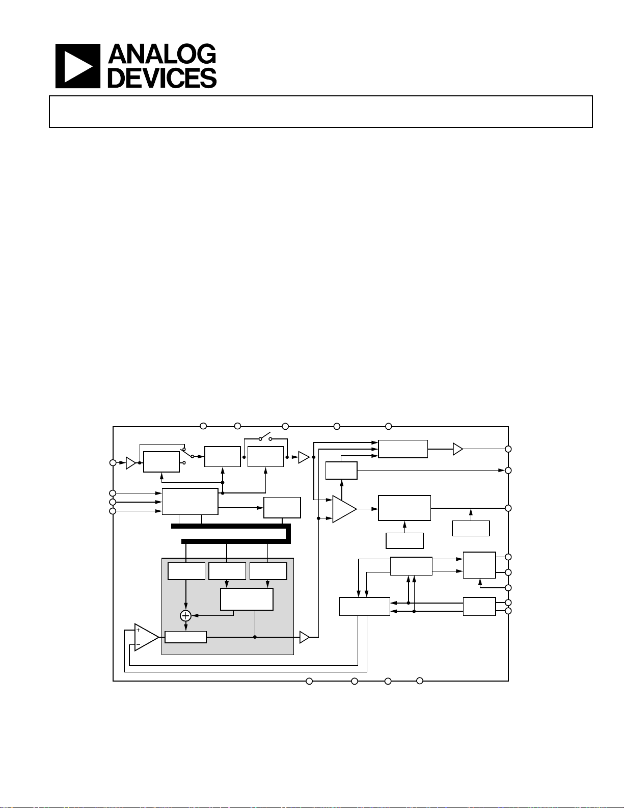
FUNCTIONAL BLOCK DIAGRAM
AV
DD
DV
Integer-N PLL Synthesizer
ADF4150HV
GENERAL DESCRIPTION
The ADF4150HV is a 3.0 GHz, fractional-N or integer-N
frequency synthesizer with an integrated high voltage charge
pump. The synthesizer can be used to drive external wideband
VCOs directly, eliminating the need for operational amplifiers
to achieve higher tuning voltages. This simplifies design and
reduces cost while improving phase noise, in contrast to active
filter topologies, which tend to degrade phase noise compared
to passive filter topologies.
The VCO frequency can be divided by 1, 2, 4, 8, or 16 to allow
the user to generate RF output frequencies as low as 31.25 MHz.
For applications that require isolation, the RF output stage can be
muted. The mute function is both pin- and software-controllable.
A simple 3-wire interface controls all on-chip registers. The
charge pump operates from a power supply ranging from 6 V to
30 V, whereas the rest of the device operates from 3.0 V to 3.6 V.
The ADF4150HV can be powered down when not in use.
DD
P
R
SET
REF
IN
CLK
DATA
LE
Rev. 0
Information furnished by Analog Devices is believed to be accurate and reliable. However, no
responsibility is assumed by Analog Devices for its use, nor for any infringements of patents or other
rights of third parties that may result from its use. Specifications subject to change without notice. No
license is granted by implication or otherwise under any patent or patent rights of Analog Devices.
Trademarks and registered trademarks are the property of their respective owners.
×2
DOUBLER
DATA REG ISTE R
N COUNTER
INTEGER
VALUE
10-BIT R
COUNTER
FRACTION
VALUE
THIRD-ORDER
FRACTIONAL
INTERPOL ATOR
÷2
DIVIDER
FUNCTION
LATCH
MODULUS
VALUE
LOCK
DETECT
PHASE
COMPARATOR
MULTIPLEXER
MULTIPLEXER
HIGH VOL TAGE
CHARGE
PUMP
CURRENT
SETTING
DIVIDE -BY-1/
-2/-4/-8/-16
BOOST
MODE
OUTPUT
STAGE
INPUT
RF
MUXOUT
LD
CP
RF
RF
PDB
RF
RF
ADF4150HV
GNDCE CP
GND
SD
GND
Figure 1.
One Technology Way, P.O. Box 9106, Norwood, MA 02062-9106, U.S.A.
Tel: 781.329.4700 www.analog.com
Fax: 781.461.3113 ©2011 Analog Devices, Inc. All rights reserved.
OUT
OUT
OUT
IN
IN
+
–
RF
+
–
09058-001
Page 2

ADF4150HV
TABLE OF CONTENTS
Features .............................................................................................. 1
Applications ....................................................................................... 1
General Description ......................................................................... 1
Functional Block Diagram .............................................................. 1
Revision History ............................................................................... 2
Specifications ..................................................................................... 3
Timing Characteristics ................................................................ 5
Absolute Maximum Ratings ............................................................ 6
Transistor Count ........................................................................... 6
Thermal Resistance ...................................................................... 6
ESD Caution .................................................................................. 6
Pin Configuration and Function Descriptions ............................. 7
Typical Performance Characteristics ............................................. 9
Circuit Description ......................................................................... 11
Reference Input Section ............................................................. 11
RF N Divider ............................................................................... 11
Phase Frequency Detector (PFD) and High Voltage
Charge Pump .............................................................................. 11
MUXOUT and Lock Detect ...................................................... 12
Input Shift Registers ................................................................... 12
Program Modes .......................................................................... 12
Output Stage ................................................................................ 12
Register Maps .................................................................................. 13
Register 0 ..................................................................................... 17
REVISION HISTORY
8/11—Revision 0: Initial Version
Register 1 ..................................................................................... 17
Register 2 ..................................................................................... 17
Register 3 ..................................................................................... 19
Register 4 ..................................................................................... 19
Register 5 ..................................................................................... 19
Register Initialization Sequence ............................................... 19
RF Synthesizer—A Worked Example ...................................... 20
Reference Doubler and Reference Divider ............................. 20
12-Bit Programmable Modulus ................................................ 20
Spurious Optimization and Boost Mode ................................ 21
Spur Mechanisms ....................................................................... 21
Spur Consistency and Fractional Spur Optimization ........... 21
Phase Resync ............................................................................... 22
Applications Information .............................................................. 23
Ultrawideband PLL .................................................................... 23
Microwave PLL ........................................................................... 23
Generating the High Voltage Supply ....................................... 24
Interfacing to the ADuC702x and the ADSP-BF527 ............. 25
PCB Design Guidelines for a Chip Scale Package ................. 25
Output Matching ........................................................................ 26
Outline Dimensions ....................................................................... 27
Ordering Guide .......................................................................... 27
Rev. 0 | Page 2 of 28
Page 3

ADF4150HV
SPECIFICATIONS
AVDD = DVDD = SDVDD = 3.3 V ± 10%; VP = 6.0 V to 30 V; GND = 0 V; TA = T
range is −40°C to +85°C.
Table 1.
Parameter Min Typ Max Unit Test Conditions/Comments
REFIN CHARACTERISTICS
Input Frequency 10 300 MHz For f < 10 MHz, ensure slew rate > 21 V/μs
10 30 MHz
Input Sensitivity 0.7 AVDD V p-p Biased at AVDD/2; ac coupling ensures AVDD/2 bias
Input Capacitance 5.0 pF
Input Current ±60 μA
RF INPUT CHARACTERISTICS
RF Input Frequency (RFIN) 0.5 3.0 GHz −10 dBm ≤ RF input power ≤ +5 dBm
Prescaler Output Frequency 750 MHz
PHASE DETECTOR
Phase Detector Frequency 26 MHz Low noise mode
20 MHz Low spur mode
26 MHz Integer-N mode
HIGH VOLTAGE CHARGE PUMP
ICP Sink/Source
High Value 384 μA R
Low Value 48 μA R
R
Range 3.3 10 kΩ
SET
High Value vs. R
196 μA R
SET
594 μA R
Sink and Source Current Matching 6 % 1.0 V ≤ VCP ≤ (VP − 1.0 V); VP = 6 V to 30 V
Absolute ICP Accuracy 3 %
ICP vs. VCP 2.5 % 1.0 V ≤ VCP ≤ (VP − 1.0 V)
ICP vs. Temperature 2.5 % VCP = VP/2
ICP Leakage 2.5 nA VCP = VP/2
LOGIC INPUTS
Input High Voltage, V
Input Low Voltage, V
Input Current, I
INH/IINL
2.0 V
INH
0.6 V
INL
±1 μA
Input Capacitance, CIN 15.0 pF
LOGIC OUTPUTS
Output High Voltage, VOH DVDD − 0.4 V CMOS output selected
Output High Current, IOH 500 μA
Output Low Voltage, VOL 0.4 V IOL = 500 μA
POWER SUPPLIES
AVDD 3.0 3.6 V
DVDD, SDVDD AVDD V
VP 6.0 30 V
IP 1 2.5 mA VP = 30 V
DIDD + AI
1
50 60 mA
DD
Current per Output Divider 6 to 24 mA Each output divide-by-2 consumes 6 mA typ
2
I
RFOUT
20 32 mA RF output stage is programmable
Low Power Sleep Mode 1 μA
MIN
to T
, unless otherwise noted. Operating temperature
MAX
Reference doubler enabled (DB25 bit in
Register 2 is set to 1)
For lower RF
frequencies, ensure slew
IN
rate > 400 V/μs
= 5.1 kΩ
SET
= 5.1 kΩ
SET
= 10 kΩ
SET
= 3.3 kΩ
SET
Set the V
supply at least 1 V above the
P
maximum desired tuning voltage
Rev. 0 | Page 3 of 28
Page 4

ADF4150HV
Parameter Min Typ Max Unit Test Conditions/Comments
RF OUTPUT CHARACTERISTICS
Output Frequency Using RF Output
Dividers
Harmonic Content (Second) −19 dBc Fundamental VCO output
−20 dBc Divided VCO output
Harmonic Content (Third) −13 dBc Fundamental VCO output
−10 dBc Divided VCO output
Minimum RF Output Power
Maximum RF Output Power
2
−4 dBm Programmable in 3 dB steps
2
5 dBm Programmable in 3 dB steps
Output Power Variation vs. Supply ±1 dB
Output Power Variation vs. Temperature ±1 dB From −40°C to +85°C
Level of Signal with RF Mute Enabled −37 dBm PDBRF pin brought low; RF = 2 GHz
NOISE CHARACTERISTICS
Normalized In-Band Phase Noise
Floor (PN
SYNTH
3
)
−203 dBc/Hz Low spur mode
Normalized 1/f Noise (PN
4
)
−113 dBc/Hz Low noise mode
1_f
−108 dBc/Hz Low spur mode
RF Output Divider Noise Floor −155 dBc/Hz Measured at 10 MHz offset
Spurious Signals Due to PFD Frequency −70 dBc At RF
−85 dBc At VCO output
1
TA = 25°C; AVDD = DVDD = 3.3 V; prescaler = 8/9; f
2
Using 50 Ω resistors to AVDD, into a 50 Ω load.
3
This figure can be used to calculate phase noise for any application. To calculate in-band phase noise performance as seen at the VCO output, use the following formula:
PN
= PN
SYNTH
4
The PLL phase noise is composed of flicker (1/f) noise plus the normalized PLL noise floor. The flicker noise is specified at a 10 kHz offset and normalized to 1 GHz. The
formula for calculating the 1/f noise contribution at an RF frequency (fRF) and at a frequency offset (f) is given by PN = PN
the normalized phase noise floor and flicker noise are modeled in ADIsimPLL.
− 10 log(f
TOT
) − 20 log N.
PFD
31.25 MHz 500 MHz VCO input and divide-by-16 selected
Pull-up supply on Pin 18 and Pin 19 varied
from 3.0 V to 3.6 V
−213 dBc/Hz Low noise mode
+/RF
− pins
OUT
+ 10 log(10 kHz/f) + 20 log(fRF/1 GHz). Both
1_f
= 100 MHz; f
REFIN
= 25 MHz; fRF = 1.75 GHz.
PFD
OUT
Rev. 0 | Page 4 of 28
Page 5
ADF4150HV
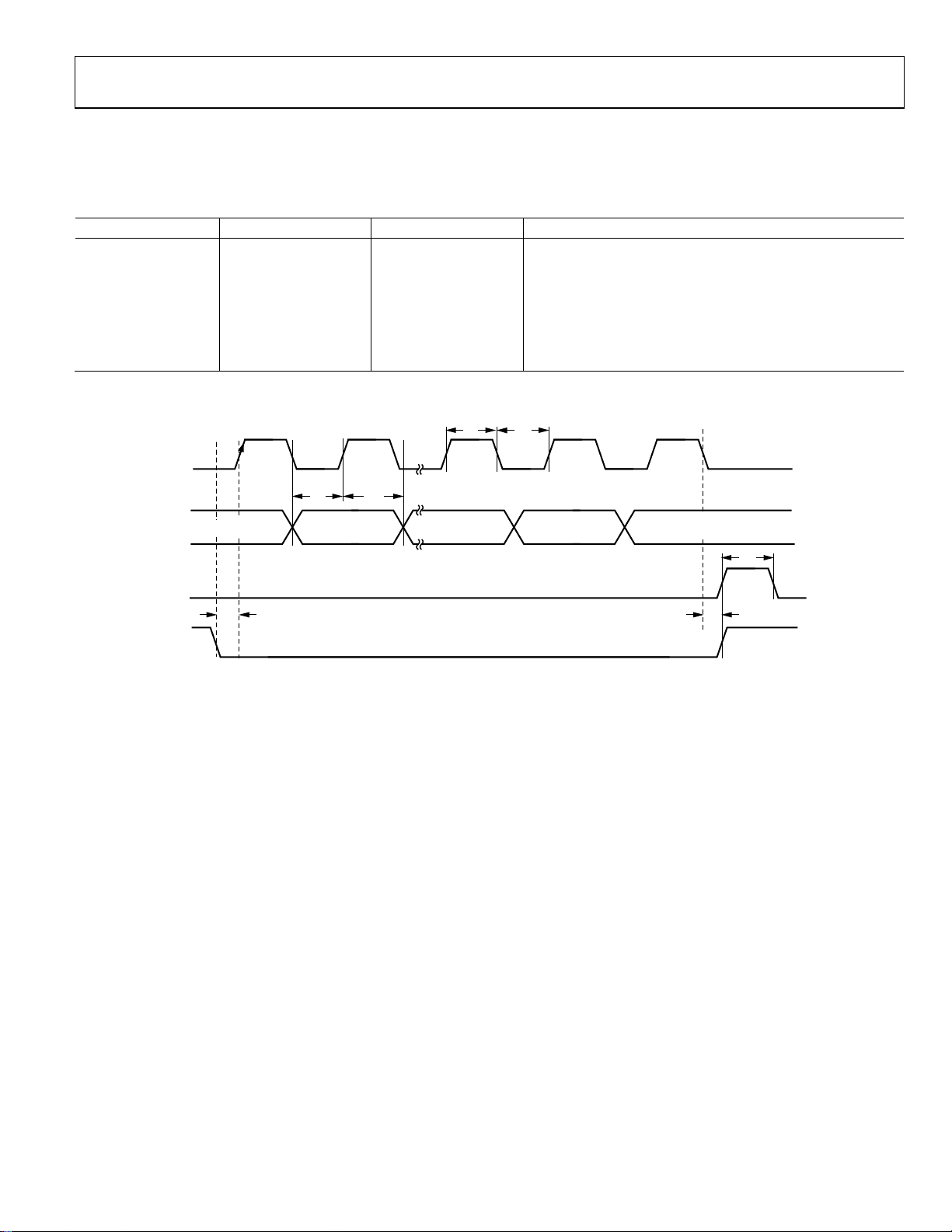
TIMING CHARACTERISTICS
AVDD = DVDD = SDVDD = 3.3 V ± 10%; VP = 6.0 V to 30 V; GND = 0 V; TA = T
range is −40°C to +85°C.
Table 2.
Parameter Limit Unit Description
t1 20 ns min LE setup time
t2 10 ns min DATA to CLK setup time
t3 10 ns min DATA to CLK hold time
t4 25 ns min CLK high duration
t5 25 ns min CLK low duration
t6 10 ns min CLK to LE setup time
t7 20 ns min LE pulse width
Timing Diagram
t
4
CLK
to T
MIN
t
5
, unless otherwise noted. Operating temperature
MAX
DATA
DB31 (MSB) DB30
LE
t
1
LE
t
2
t
3
DB2
(CONTROL BIT C3)
DB1
(CONTROL BIT C2)
DB0 (LSB)
(CONTROL BIT C1)
t
6
t
7
09058-002
Figure 2. Timing Diagram
Rev. 0 | Page 5 of 28
Page 6
ADF4150HV
ABSOLUTE MAXIMUM RATINGS
TA = 25°C, unless otherwise noted.
Table 3.
Parameter Rating
AVDD to GND1 −0.3 V to +3.9 V
AVDD to DVDD −0.3 V to +0.3 V
VP to GND1 −0.3 V to +33 V
Digital I/O Voltage to GND1 −0.3 V to AVDD + 0.3 V
Analog I/O Voltage to GND1 −0.3 V to DVDD + 0.3 V
REFIN to GND1 −0.3 V to AVDD + 0.3 V
Operating Temperature Range −40°C to +85°C
Storage Temperature Range −65°C to +125°C
Maximum Junction Temperature 150°C
Reflow Soldering
Peak Temperature 260°C
Time at Peak Temperature 40 sec
1
GND = CP
GND
= SD
GND
= 0 V.
Stresses above those listed under Absolute Maximum Ratings
may cause permanent damage to the device. This is a stress
rating only; functional operation of the device at these or any
other conditions above those indicated in the operational
section of this specification is not implied. Exposure to absolute
maximum rating conditions for extended periods may affect
device reliability.
TRANSISTOR COUNT
The transistor count for the ADF4150HV is 23,380 (CMOS)
and 809 (bipolar).
THERMAL RESISTANCE
Thermal impedance (θJA) is specified for a device with the
exposed pad soldered to GND.
Table 4. Thermal Resistance
Package Type θJA Unit
32-Lead LFCSP (CP-32-11) 27.3 °C/W
ESD CAUTION
Rev. 0 | Page 6 of 28
Page 7
ADF4150HV
–
A
PIN CONFIGURATION AND FUNCTION DESCRIPTIONS
SDVDDMUXOUTLDREF
–
+
DD
IN
IN
AV
RF
RF
IN
25
GND
24 GND
23
GND
DV
22
PDB
21
20
AV
19
RF
18
RF
17 GND
DD
DD
OUT
OUT
RF
+
09058-003
GND
SET
GND
R
GND
SD
32313029282726
GND
1
2
CLK
DAT
3
4
5
6
P
7
8
ADF4150HV
TOP VIEW
(Not to Scale)
9
10111213141516
DD
OUT
GND
GND
AV
CP
CP
LE
CE
V
GND
GND
NOTES
1. THE LFCSP HAS AN EXPO SED PAD
THAT MUST BE CONNECTED TO GND.
Figure 3. Pin Configuration
Table 5. Pin Function Descriptions
Pin No. Mnemonic Description
1, 7, 8, 12, 16, 17,
GND Ground. All ground pins should be tied together.
23, 24, 30, 32
2 CLK
Serial Clock Input. Data is clocked into the 32-bit shift register on the CLK rising edge. This input is a high
impedance CMOS input.
3 DATA
Serial Data Input. The serial data is loaded MSB first with the three LSBs as the control bits. This input is a
high impedance CMOS input.
4 LE
Load Enable. When LE goes high, the data stored in the 32-bit shift register is loaded into the register
that is selected by the three control bits. This input is a high impedance CMOS input.
5 CE
6 VP
Chip Enable. A logic low on this pin powers down the device and puts the charge pump into three-state
mode. A logic high on this pin powers up the device.
High Voltage Charge Pump Power Supply. Place decoupling capacitors to the ground plane as close to
this pin as possible. The decoupling capacitors should have the appropriate voltage rating (a value of
10 μF is recommended). Care should be taken to ensure that V
does not exceed the absolute maximum
P
ratings on power-up (see Table 3 ). A 10 Ω series resistor can help to significantly reduce voltage overshoot
with minimal IR drop.
9 CP
10 CP
11, 13, 20 AVDD
OUT
High Voltage Charge Pump Output. When enabled, this output provides ±I
filter. The output of the loop filter is connected to the voltage tuning port of the external VCO.
High Voltage Charge Pump Ground. All ground pins should be tied together.
GND
Analog Power Supply. This pin ranges from 3.0 V to 3.6 V. Place decoupling capacitors to the ground
plane as close to this pin as possible. AV
must have the same value as DVDD.
DD
to the external passive loop
CP
14 RFIN+ Positive RF Input. The output of the VCO or external prescaler should be ac-coupled to this pin.
15 RFIN−
Complementary RF Input. If a single-ended input is required, this pin can be tied to ground via a 100 pF
capacitor.
18 RF
OUT
−
Divided-Down Output of RF
−. This pin can be left unconnected if the divider functionality is not
IN
required.
19 RF
OUT
+
Divided-Down Output of RF
+. This pin can be left unconnected if the divider functionality is not
IN
required.
21 PDBRF RF Power-Down. A logic low on this pin mutes the RF outputs. This function is also software controllable.
22 DVDD
25 REFIN
Digital Power Supply. Place decoupling capacitors to the ground plane as close to this pin as possible.
must have the same value as AVDD.
DV
DD
Reference Input. This CMOS input has a nominal threshold of AV
/2 and a dc equivalent input resistance
DD
of 100 kΩ. This input can be driven from a crystal oscillator, TCXO, or other reference.
26 LD
Lock Detect Output. A logic high output on this pin indicates PLL lock. A logic low output indicates loss
of PLL lock.
Rev. 0 | Page 7 of 28
Page 8

ADF4150HV
Pin No. Mnemonic Description
27 MUXOUT
28 SDVDD
29 SD
31 R
Digital Σ-Δ Modulator Ground. All ground pins should be tied together.
GND
SET
EP Exposed Pad Exposed Pad. The LFCSP has an exposed pad that must be connected to GND.
Multiplexer Output. The multiplexer output allows the lock detect, the N divider value, or the R counter
value to be accessed externally.
Digital Σ-Δ Modulator Power Supply. Place decoupling capacitors to the ground plane as close to this
pin as possible. SDVDD must have the same value as AVDD.
Connecting a resistor between this pin and GND sets the charge pump output current. Place the resistor
as close to this pin as possible. The nominal voltage bias at the R
I
and R
CP
is as follows:
SET
ICP = 1.96/R
SET
pin is 0.55 V. The relationship between
SET
where:
= 5.1 kΩ.
R
SET
I
= 384 μA.
CP
Rev. 0 | Page 8 of 28
Page 9
ADF4150HV
–
–
–
TYPICAL PERFORMANCE CHARACTERISTICS
600
550
500
450
400
350
300
250
200
150
100
50
(µA)
0
CP
I
–50
–100
–150
–200
–250
–300
–350
–400
–450
–500
0 2 4 6 8 10121416182022242628
ICP = 400µ A SOURCE
ICP = 350µ A SOURCE
ICP = 300µ A SOURCE
ICP = 250µ A SOURCE
ICP = 200µ A SOURCE
ICP = 150µ A SOURCE
ICP = 100µ A SOURCE
ICP = 50µA SOURCE
ICP = 50µA SINK
ICP = 100µA SINK
ICP = 150µA SINK
ICP = 200µA SINK
ICP = 250µA SINK
ICP = 300µA SINK
ICP = 350µA SINK
ICP = 400µA SINK
VCP (V)
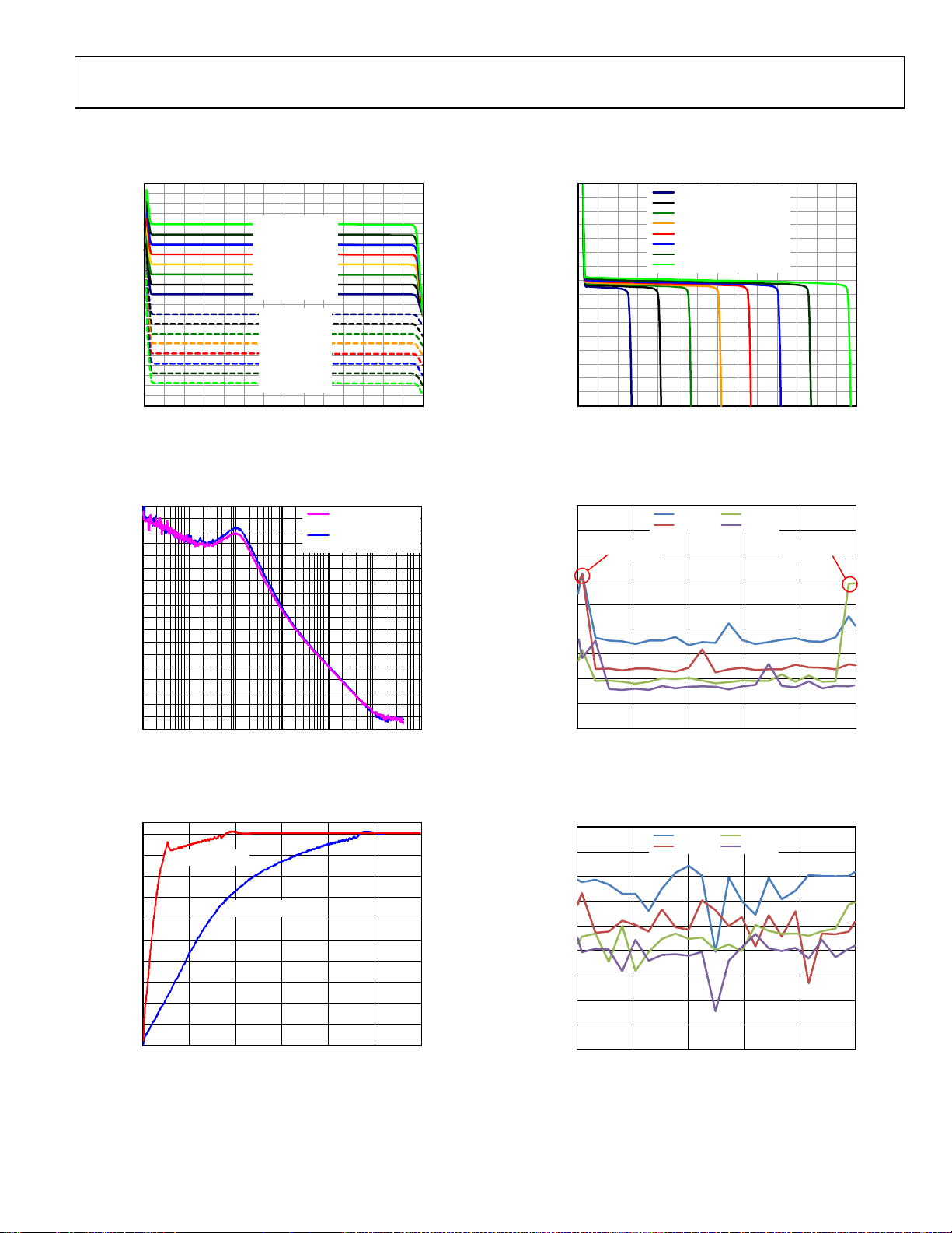
Figure 4. Charge Pump Output Characteristics, VP = 28 V,
Varied from 50 μA to 400 μA, R
I
CP
= 5.1 kΩ
SET
09058-004
16
14
12
10
8
6
4
2
0
–2
MISMATCH (%)
–4
CP
I
–6
–8
–10
–12
–14
–16
0 2 4 6 8 10121416182022242628
VP = 6V MISMATCH (%)
VP = 9V MISMATCH (%)
VP = 12V MISMATCH (%)
VP = 15V MISMATCH (%)
VP = 18V MISMATCH (%)
VP = 21V MISMATCH (%)
VP = 24V MISMATCH (%)
VP = 28V MISMATCH (%)
VCP (V)
Figure 7. Charge Pump Output Mismatch vs. VP, ICP = 200 μA
09058-007
80
–85
–90
–95
–100
–105
–110
–115
–120
–125
–130
–135
–140
PHASE NOISE (d Bc/Hz)
–145
–150
–155
–160
–165
–170
100 1k 10k 100k 1M 10M 100M
FREQUENCY (Hz)
ADF4150HV
RMS NOISE = 0.28°
ADF4156
RMS NOISE = 0.36°
Figure 5. Active Filter Phase Noise, ADF4150HV vs. ADF4156;
Active Filter Implemented Using OP27 Op Amp; PFD = 20 MHz, Loop
Bandwidth = 10 kHz, I
2.0
1.9
1.8
1.7
1.6
1.5
1.4
FREQUENCY (GHz)
1.3
1.2
1.1
1.0
0 50 100 150 200 250 300
= 300 μA, Carrier Frequency = 1.7 GHz, VP = 28 V
CP
BOOST MODE ON
BOOST MODE O FF
TIME (µs)
Figure 6. PLL Lock Time with Boost Mode On and Off;
Locking over Octave Range Jump (1 GHz to 2 GHz) for PFD = 20 MHz,
Loop Bandwidth = 100 kHz, I
= 300 μA, VP = 28 V, VDD = 3.3 V, REFIN = 100 MHz
CP
40
–50
BEAT NOTE
–60
–70
–80
–90
–100
SPUR LEVEL (dBc)
–110
–120
–130
1500 15251520151515101505
09058-005
SPUR
200kHz
400kHz
FREQUE NCY (MHz)
600kHz
800kHz
BEAT NOTE
SPUR
09058-008
Figure 8. Fractional Spur Levels vs. Frequency, Low Spur Mode;
Measured at VCO Output, PFD = 25 MHz, MOD = 125
40
–50
–60
–70
–80
–90
–100
SPUR LEVEL (dBc)
–110
–120
–130
09058-006
1500 15251520151515101505
200kHz
400kHz
FREQUENCY (MHz)
600kHz
800kHz
09058-009
Figure 9. Fractional Spur Levels vs. Frequency, Low Noise Mode;
Measured at VCO Output, PFD = 25 MHz, MOD = 125
Rev. 0 | Page 9 of 28
Page 10

ADF4150HV
–
–
–
–50
–60
–70
40
25MHz
50MHz
75MHz
100MHz
–85
–90
80
LOW SPUR MODE
–80
–90
SPUR LEVEL (dBc)
–100
–110
–120
1000 20001800160014001200
FREQUENCY (MHz )
Figure 10. PFD and Reference Spur Levels vs. Frequency at VCO Output,
= 100 MHz, PFD = 25 MHz
REF
IN
40
–50
–60
–70
–80
–90
SPUR LEVEL (dBc)
–100
–110
–120
1000 20001800160014001200
25MHz
50MHz
FREQUENCY (MHz )
75MHz
100MHz
Figure 11. PFD and Reference Spur Levels vs. Frequency at VCO Output
with ADL5541 Buffer Placed Between VCO Output and RF Input,
REF
= 100 MHz, PFD = 25 MHz
IN
–95
–100
PHASE NOISE (d Bc/Hz)
–105
–110
1000 130012501200115011001050
09058-110
LOW NOI SE MODE
FREQUENCY (MHz )
09058-112
Figure 12. In-Band Phase Noise Measured at 3 kHz Offset for Low Noise Mode
and Low Spur Mode, PFD = 25 MHz, PLL Loop Bandwidth = 40 kHz
4
2
0
–2
–4
–6
–8
–10
OUTPUT PO WER (dBm)
–12
–14
–16
0 2500200015001000500
09058-111
+5dBm
+2dBm
–1dBm
–4dBm
FREQUENCY (MHz )
09058-113
Figure 13. Single-Ended RF Output Power Level vs. Frequency and
Power Setting, RF Output Pins Pulled Up to 3.3 V via 27 nH||50 Ω
Rev. 0 | Page 10 of 28
Page 11

ADF4150HV
O
CIRCUIT DESCRIPTION
REFERENCE INPUT SECTION
The reference input stage is shown in Figure 14. The SW1 and
SW2 switches are normally closed. The SW3 switch is normally
open. When power-down is initiated, SW3 is closed, and SW1
and SW2 are opened. In this way, no loading of the REF
IN
pin
occurs during power-down.
POWER-DOWN
CONTROL
100kΩ
NC
REF
SW1
NO
SW2
SW3
NC
IN
Figure 14. Reference Input Stage
BUFFER
TO R COUNT ER
09058-010
RF N DIVIDER
The RF N divider allows a division ratio in the PLL feedback
path. The division ratio is determined by the INT, FRAC, and
MOD values, which build up this divider (see Figure 15).
FROM
VCO OUTPUT/
UTPUT DIVIDE RS
RF N DIVIDER
N COUNTER
INT
VALUE
N = INT + FRAC/ MOD
THIRD-ORDER
FRACTIONAL
INTERPOL ATOR
MOD
VALUE
FRAC
VALUE
TO PFD
The PFD frequency (f
= REFIN × [(1 + D)/(R × (1 + T))] (2)
f
PFD
where:
REF
is the reference input frequency.
IN
D is the REF
doubler bit.
IN
R is the preset divide ratio of the binary 10-bit programmable
reference counter (1 to 1023).
T is the REF
divide-by-2 bit (0 or 1).
IN
Integer-N Mode
If FRAC = 0 and the DB8 (LDF) bit in Register 2 is set to 1,
the synthesizer operates in integer-N mode. The DB8 bit in
Register 2 should be set to 1 for integer-N digital lock detect.
R Counter
The 10-bit R counter allows the input reference frequency
) to be divided down to produce the reference clock
(REF
IN
to the PFD. Division ratios from 1 to 1023 are allowed.
PHASE FREQUENCY DETECTOR (PFD) AND HIGH VOLTAGE CHARGE PUMP
The phase frequency detector (PFD) takes inputs from the
R counter and N counter and produces an output proportional
to the phase and frequency difference between them. Figure 16
is a simplified schematic of the phase frequency detector.
HIGH
U1
+IN
CLR1
PFD
UP
Q1D1
) equation is
09058-011
Figure 15. RF N Divider
INT, FRAC, MOD, and R Counter Relationship
The INT, FRAC, and MOD values, in conjunction with the
R counter, make it possible to generate output frequencies that
are spaced by fractions of the PFD frequency. For more information, see the RF Synthesizer—A Worked Example section.
The RF VCO frequency (RF
= (f
RF
OUT
/RF Divider) × [INT + (FRAC/MOD)] (1)
PFD
) equation is
OUT
where:
RF
is the output frequency of the external voltage controlled
OUT
oscillator (VCO).
RF Divider is the output divider that divides down the VCO
frequency.
INT is the preset divide ratio of the binary 16-bit counter (23 to
32,767 for the 4/5 prescaler, 75 to 65,535 for the 8/9 prescaler).
FRAC is the numerator of the fractional division (0 to MOD − 1).
MOD is the preset fractional modulus (2 to 4095).
HIGH
–IN
CLR2
U2
DELAY
DOWN
Q2D2
U3
CHARGE
PUMP
CP
OUT
09058-012
Figure 16. PFD Simplified Schematic
The PFD includes a delay element that sets the width of the
antibacklash pulse to 4.2 ns. This pulse ensures that there is
no dead zone in the PFD transfer function and provides a
consistent reference spur level.
The high voltage charge pump is designed on an Analog
Devices, Inc., proprietary high voltage process and allows the
charge pump to output voltages as high as 29 V when powered
by a 30 V supply. The high voltage charge pump removes the
need for active filtering when interfacing to a high voltage VCO.
Rev. 0 | Page 11 of 28
Page 12

ADF4150HV
–
MUXOUT AND LOCK DETECT
The multiplexer output on the ADF4150HV allows the user to
access various internal points on the chip. The state of MUXOUT is
controlled by the M3, M2, and M1 bits in Register 2 (see Figure 22).
Figure 17 shows the MUXOUT section in block diagram form.
THREE-STATE-OUTPUT
DV
GND
R COUNTER OUTP UT
N COUNTER OUTP UT
ANALOG LOCK DETECT
DIGITAL LOCK DETECT
RESERVED
R COUNTER INPUT
DD
MUX
Figure 17. MUXOUT Schematic
CONTROL
DV
GND
DD
MUXOUT
09058-013
INPUT SHIFT REGISTERS
The ADF4150HV digital section includes a 10-bit RF R counter,
a 16-bit RF N counter, a 12-bit FRAC counter, and a 12-bit
modulus counter. Data is clocked into the 32-bit shift register
on each rising edge of CLK. The data is clocked in MSB first.
Data is transferred from the shift register to one of six latches
on the rising edge of LE. The destination latch is determined by
the state of the three control bits (C3, C2, and C1) in the shift
register. As shown in Figure 2, the control bits are the three LSBs:
DB2, DB1, and DB0. The truth table for these bits is shown in
Table 6. Figure 19 summarizes how the latches are programmed.
Table 6. Truth Table for C3, C2, and C1 Control Bits
Control Bits
Register C3 C2 C1
0 0 0 Register 0 (R0)
0 0 1 Register 1 (R1)
0 1 0 Register 2 (R2)
0 1 1 Register 3 (R3)
1 0 0 Register 4 (R4)
1 0 1 Register 5 (R5)
PROGRAM MODES
Table 6 and Figure 19 through Figure 25 show how the program
modes are set up in the ADF4150HV.
The following settings in the ADF4150HV are double buffered:
phase value, modulus value, reference doubler, reference divideby-2, R counter value, and charge pump current setting. Before
the part uses a new value for any double-buffered setting, the
following two events must occur:
1. The new value is latched into the device by writing to the
appropriate register.
2. A new write is performed on Register 0 (R0).
For example, any time that the modulus value is updated,
Register 0 (R0) must be written to, to ensure that the modulus
value is loaded correctly. The divider select value in Register 4
(R4) is also double buffered, but only if the DB13 bit of
Register 2 (R2) is high.
OUTPUT STAGE
The RF
to the collectors of an NPN differential pair driven by buffered
outputs of the VCO, as shown in Figure 18. To allow the user to
optimize the power dissipation vs. output power requirements,
the tail current of the differential pair is programmable using
Bits[DB4:DB3] in Register 4 (R4). Four current levels can be set.
These levels give output power levels of −4 dBm, −1 dBm, +2 dBm,
and +5 dBm, respectively, using a 50 Ω resistor to AV
coupling into a 50 Ω load. Alternatively, both outputs can be
combined in a 1 + 1:1 transformer or a 180° microstrip coupler
(see the Output Matching section). If the outputs are used
individually, the optimum output stage consists of a shunt
inductor to AV
Another feature of the ADF4150HV is that the supply current to
the RF output stage can be shut down until the part achieves lock,
as measured by the digital lock detect circuitry. This feature is
enabled by the mute-till-lock detect (MTLD) bit in Register 4 (R4).
+ and RF
OUT
VCO
− pins of the ADF4150HV are connected
OUT
.
DD
+RF
RF
OUT
BUFFER/
DIVIDE-BY-1/-2/-4/-8/-16
Figure 18. Output Stage
OUT
and ac
DD
09058-014
Rev. 0 | Page 12 of 28
Page 13

ADF4150HV
REGISTER MAPS
REGISTER 0
RESERVED
DB31
DB30 DB29 DB28 DB27 DB26 DB25 D B24 DB2 3 DB22 DB21 DB20 DB19 DB18 DB17 DB16 DB15 DB14 DB13 DB12 DB11 DB10 DB9 DB8 DB7 DB6 DB5 DB4 DB3 DB2 DB1 DB0
0
N16 N15 N14 N13 N12 N11 N10 N9
16-BIT INTEGER VALUE (INT) 12-BIT FRACTIONAL VALUE (FRAC)
N8 N7 N6 N5 N4 N3 N2 N1 F12 F11 F1 0 F9 F8 F7 F6 F5 F4 F3 F2 F1 C3(0) C2(0) C1(0)
CONTRO L
BITS
REGISTER 1
RESERVED
DB31 DB30 DB29 D B28 DB27 DB26 DB25 DB24 DB23 DB22 DB21 DB20 DB19 DB18 DB17 DB16 DB15 DB1 4 DB13 DB12 DB11 DB10 DB9 DB8 D B7 DB6 DB5 DB4 DB3 DB2 DB1 DB0
0000PR1P12P11P10P9
LOW
NOISE AND
LOW SPUR
MODES
RESERVED
DB31 DB30 DB29 D B28 DB27 DB26 DB25 DB24 DB23 DB22 DB21 DB20 DB19 DB18 DB17 DB16 DB15 DB1 4 DB13 DB12 DB11 DB10 DB9 DB8 D B7 DB6 DB5 DB4 DB3 DB2 DB1 DB0
0 L2 L 1 M3 M2 M1 RD2 RD1 R10 R9 R8 R7 R6 R5 R4 R3 R2 R1 D1 0 CP3 CP2 CP1 U6 U5 1 U3 U2 U1 C3(0) C2(1) C1(0)
PRESCALER
MUXOUT
12-BIT PHASE VALUE (P HASE) 12-BIT MODULU S VALUE (MO D)
P8 P7 P6 P5 P4 P3 P2 P1 M12 M11 M10 M9 M8 M7 M 6 M5 M4 M 3 M 2 M1 C3(0) C2( 0) C1(1)
1
1
DBR
DBR
RDIV2
REFERENCE
DOUBLER
10-BIT R COUNTER
1
DBR
REGISTER 2
DBR
1
DBR
CHARGE
PUMP
1
DOUBLE
BUFFER
CURRENT
SETTING
RESERVED
LDP
LDF
1
DBR
RESERVED
POWER-DOW N
CP THREE-
CONTROL
BITS
CONTROL
STATE
COUNTER
RESET
BITS
REGISTER 3
CLK
RESERVED
DB31 DB30 DB29 D B28 DB27 DB26 DB25 DB24 DB23 DB22 DB21 DB20 DB19 DB18 DB17 DB16 DB15 DB1 4 DB13 DB12 DB11 DB10 DB9 DB8 D B7 DB6 DB5 DB4 DB3 DB2 DB1 DB0
0 0 0 0 0 0 0 0 0 0 0 0 0 B1 0 C2 C1 D12 D11 D10 D9 D8 D7 D6 D5 D4 D3 D2 D1 C3(0 ) C2(1) C1(1)
BOOST EN
RESERVED
DIV
MODE
12-BI T CLOCK DI VIDER VALUE
CONTROL
BITS
REGISTER 4
2
DBB
RESERVED
DB31 DB30 DB29 DB28 DB2 7 DB26 DB25 DB24 DB23 DB22 DB21 DB20 DB19 DB18 DB17 DB16 DB15 DB 14 DB13 DB12 DB11 DB10 DB9 DB8 DB7 DB6 DB5 DB4 DB3 DB2 DB1 DB0
0 0 0 0 0 0 0 0 D13 D12 D11 D10 0 0 0 0 000000000 D8 D3 D2 D1 C3(1) C2(0) C1(0)
DIVIDER
SELECT
FEEDBACK
SELECT
RESERVED RESERVED
MTLD
RF OUTPUT
OUTPUT
POWER
ENABLE
CONTRO L
BITS
REGISTER 5
RESERVED
RESERVED
CC ENABLE
ABP
WIDTH
DB31 DB30 DB29 DB28 DB27 DB26 DB25 DB24 DB23 DB22 DB21 DB20 DB19 DB18 DB17 DB16 DB15 DB1 4 DB13 DB12 DB11 DB10 DB9 DB8 DB7 DB6 DB5 DB4 DB3 DB2 DB1 DB0
ABP2 ABP1 CE1 1 0 0 0 0 D 15 D14 0 0 0 0 0 0 0 0 0 0 0 0 0 0 0 0 0 0 0 C3(1) C2(0) C1(1)
1
DBR = DOUBL E BUFF ERED RE GIST ER—BUF FERED B Y THE WRITE TO REGIS TER 0.
2
DBB = DOUBLE BUFF ERED BITS— BUFFERED BY THE WRIT E TO REGISTER 0, IF AND ONLY IF DB13 OF REGISTER 2 I S HIGH.
LD PIN
MODE
RESERVED
CONTRO L
BITS
Figure 19. Register Summary
Rev. 0 | Page 13 of 28
09058-015
Page 14

ADF4150HV
RESERVED
DB31
DB30 DB2 9 DB28 DB27 DB26 DB25 DB2 4 DB23 DB2 2 DB21 DB20 DB19 DB18 DB17 DB16 DB15 DB14 DB13 DB1 2 DB11 DB10 DB9 DB8 DB7 DB6 DB5 D B4 DB3 DB2 DB1 DB0
0
N16 N15 N14 N13 N12 N11 N10 N9
16-BIT INTEG ER VALUE (INT) 12-BIT FRACTIO NAL VALUE (FRAC)
N8 N7 N6 N5 N4 N3 N2 N1 F12 F11 F10 F9 F8 F7 F6 F5 F4 F3 F2 F1 C3(0) C2(0 ) C1(0)
N16 N15 ... N5 N4 N3 N2 N1 INTEGER VALUE (INT )
00...00000 NOTALLOWED
00...00001 NOTALLOWED
00...00010 NOTALLOWED
.......... ...
00...10110 NOTALLOWED
00...10111 23
00...11000 24
.......... ...
11...11101 65,533
11...11110 65,534
11...11111 65,535
INTmin = 75 WITH PRESCALER = 8/ 9
F12 F11 ... F2 F1 FRACTIONA L VALUE (FRAC)
00...00 0
00...01 1
00...10 2
00...11 3
....... .
....... .
....... .
1 1 . .. 0 0 4092
1 1 . .. 0 1 4093
1 1 . .. 1 0 4094
1 1 . .. 1 1 4095
CONTRO L
BITS
Figure 20. Register 0 (R0)
RESERVED
DB31 DB30 DB29 DB28 DB27 DB26 DB25 DB24 DB23 DB 22 DB21 DB20 DB19 DB18 DB17 DB16 DB15 DB14 DB13 DB12 DB11 DB10 DB9 DB8 DB7 DB6 DB5 DB4 DB3 DB2 DB1 DB0
0000PR1P12P11P10P9
PRESCALER
12-BIT PHASE VALUE (P HASE) 12-BIT MODULUS VALUE (MO D)
P8 P7 P6 P5 P4 P3 P2 P1 M12 M11 M10 M9 M8 M7 M6 M 5 M4 M3 M 2 M 1 C3( 0) C2(0) C1(1)
DBR DBR
CONTRO L
BITS
09058-016
P1 PRESCALER
04/5
18/9
P12 P11 ... P2 P1 PHASE VALUE (PHASE)
0 0 ... 0 0 0
0 0 ... 0 1 1 (RECO MMENDED)
0 0 ... 1 0 2
0 0 ... 1 1 3
. . ... . . .
. . ... . . .
. . ... . . .
1 1 ... 0 0 4092
1 1 ... 0 1 4093
1 1 ... 1 0 4094
1 1 ... 1 1 4095
M12 M11 ...
00 102
00 113
.. ...
.. ...
.. ...
1 1 0 0 4092
1 1 0 1 4093
1 1 1 0 4094
1 1 1 1 4095
M2 M1 INTERPOLATOR MODULUS (MOD)
...
...
...
...
...
...
...
...
...
09058-017
Figure 21. Register 1 (R1)
Rev. 0 | Page 14 of 28
Page 15

ADF4150HV
DBR
RESERVED
CHARGE
PUMP
CURRENT
SETTING
LDF
CONTROL
COUNTER
RESET
BITS
CP THREE-
LDP
RESERVED
STATE
POWER- DOWN
LOW
NOISE AND
LOW SPUR
RESERVED
MODES
DB31 DB30 DB29 DB28 DB2 7 DB2 6 DB25 DB24 DB23 DB22 DB21 DB20 DB19 DB18 DB17 DB16 DB15 DB14 DB13 DB12 DB11 DB10 DB9 DB8 DB7 DB6 DB5 DB4 DB3 DB2 DB1 DB 0
0 L2 L1 M3 M 2 M1 RD2 RD1 R10 R9 R8 R7 R6 R5 R4 R3 R2 R1 D1 0 CP3 CP2 CP1 U6 U5 1 U3 U2 U1 C3(0) C2(1) C1(0)
MUXOUT
RDIV2 DBR
REFERENCE
DOUBLER DBR
10-BIT R COUNT ER DBR
DOUBLE
BUFFER
L2 L1 NOISE MODE
00LOWNOISEMODE
0 1 RESERVED
1 0 RESERVED
11LOWSPURMODE
M3 M2 M1 OUTPUT
0 0 0 T HREE-STAT E OUTPUT
00 1DV
01 0GND
0 1 1 R COUNTER OUT PUT
1 0 0 N DI VIDER OUTPUT
1 0 1 AN ALOG LOCK DETE CT
1 1 0 DI GITAL LO CK DETECT
1 1 1 RESERVED
DD
REFERENCE
RD2
DOUBLER
0DISABLED
1ENABLED
RD1 REFERENCE DIVI DE-B Y-2
0 DISABLED
1 ENABLED
R10 R9 ...
00 011
00 102
.. ...
.. ...
.. ...
1 1 0 0 1020
1 1 0 1 1021
1 1 1 0 1022
1 1 1 1 1023
R2 R1 R COUNTER (R)
...
...
...
...
...
...
...
...
...
DOUBLE BUF FER
D1
R4[DB22: DB20]
0DISABLED
1 E NABLED
CP3 CP2 CP1
00048
00196
010144
011192
100240
101288
110336
111384
Figure 22. Register 2 (R2)
ICP(µA)
5.1kΩ
U6 L DF
0FRAC-N
1INT-N
U5 LDP
010ns
16ns
RESERVED
BIT
0 RESERVE D
1NORMAL
OPERATION
COUNTER
U1
RESET
0DISABLED
1ENABLED
CP
U2
THREE-ST ATE
0DISABLED
1ENABLED
U3 POWER- DOWN
0DISABLED
1ENABLED
09058-018
CLK
DIV
RESERVED
DB31 DB30 DB29 DB28 DB27 DB26 DB25 DB24 DB23 DB 22 DB21 DB20 DB19 DB18 DB17 DB16 DB15 DB14 DB13 DB12 DB11 DB10 DB9 DB8 DB7 DB6 DB5 DB4 DB3 DB2 DB 1 DB0
0 0 0 0 0 0 0 0 0 B1 0 C2 C1 D12 D 11 D1 0 D9 D8 D7 D6 D5 D4 D3 D2 D1 C3(0) C2(1 ) C1(1)
00
0
C2 C 1 CLOCK DI VIDER MO DE
0 0 CLO CK DIVIDER OFF
0 1 RESE RVED
1 0 RESYNC ENABL E
1 1 RESE RVED
BOOST EN
0
BOOST
B1
ENABLE
0 DISABLED
1 ENABLED
RESERVED
MODE
D12 D11 ... D2 D1 CLOCK DIVI DER VALUE
00...00 0
00...01 1
00...10 2
00...11 3
....... .
....... .
....... .
1 1 ... 0 0 4092
1 1 ... 0 1 4093
1 1 ... 1 0 4094
1 1 ... 1 1 4095
CONTRO L
BITS12-BIT CLOCK DI VIDER VALUE
Figure 23. Register 3 (R3)
Rev. 0 | Page 15 of 28
09058-019
Page 16

ADF4150HV
DBB
RESERVED
DB31 DB30 DB29 DB28 DB27 DB26 DB25 DB24 DB23 DB22 DB21 DB20 DB19 DB18 DB17 DB16 DB15 DB14 DB13 DB12 DB11 DB10 DB9 DB8 DB7 DB6 DB5 DB4 DB3 DB2 DB1 DB0
0 0 0 0 0 0 0 0 D13 D12 D11 D10 0 0 0 0 0 0 0 0 0 D8 0 0 0 0 D3 D2 D1 C3(1) C2(0) C1(0)
FEEDBACK
D13
SELECT
0
DIVIDED
FUNDAMENTAL
1
D12 D11 RF DIVIDER SELECT
00 ÷1
00 ÷2
01 ÷4
01 ÷8
10 ÷160
DIVIDER
SELECT
FEEDBACK
SELECT
D10
0
1
0
1
RESERVED RESERVED
MUTE TILL
D8
LOCK DETECT
0 MUTE DISABLED
1 MUTE ENABLED
MTLD
Figure 24. Register 4 (R4)
OUTPUT
POWER
RF OUTPUT
ENABLE
D2 D1 OUTPUT POW ER ( dBm )
00–4
01–1
10+2
11+5
D3 RF OUT
0 DISABLED
1 ENABLED
CONTROL
BITS
09058-020
ABP
WIDTH
DB31 DB30 DB29 DB28 DB27 DB26 DB25 DB24 DB23 DB22 DB21 DB20 DB19 DB18 DB17 DB16 DB15 DB14 DB13 DB12 DB11 DB10 DB9 DB8 DB7 DB6 DB5 DB4 DB3 DB2 DB1 DB0
ABP2ABP1CE110000D15D140000000000000000000C3(1)C2(0)C1(1)
ABP2 ABP1 ANTI BAC KLAS H PU LS E WIDTH
0 0 4.2ns ( RECOMM ENDED)
0 1 RESE RVED
1 0 RESE RVED
1 1 RESE RVED
1
MUXOUT IN REGISTER 2 MUST ALSO BE SET TO DIGITAL LOCK DETECT FOR THE LO CK DETECT PINTO OPERATE CORRECTLY.
RESERVED
CC ENABLE
D15 D14 LOCK DETECT PIN OPERATION
0 0 OUTPUT LOW
0 1 DIG I TAL LOCK DETECT
1 0 OUTPUT LOW
11OUTPUT HIGH
RESERVED BIT
0 RESERVED
1 NO RMAL OPERATIO N
CE1 CHARGE CANCELL ATION
0DISABLED
1 ENABLED
LD PIN
MODE
1
CONTROL
BITSRESERVEDRESERVED
Figure 25. Register 5 (R5)
09058-021
Rev. 0 | Page 16 of 28
Page 17

ADF4150HV
REGISTER 0
Control Bits
When Bits[C3:C1] are set to 000, Register 0 is programmed.
Figure 20 shows the input data format for programming this
register.
16-Bit Integer Value (INT)
The 16 INT bits (Bits[DB30:DB15]) set the INT value, which
determines the integer part of the feedback division factor. The
INT value is used in Equation 1 (see the INT, FRAC, MOD, and
R Counter Relationship section). Integer values from 23 to
32,767 are allowed for the 4/5 prescaler; for the 8/9 prescaler,
the minimum integer value is 75 and the maximum value is
65,535.
12-Bit Fractional Value (FRAC)
The 12 FRAC bits (Bits[DB14:DB3]) set the numerator of the
fraction that is input to the Σ- modulator. This fraction, along
with the INT value, specifies the new frequency channel that
the synthesizer locks to, as shown in the RF Synthesizer—A
Work e d E x ampl e section. FRAC values from 0 to (MOD − 1)
cover channels over a frequency range equal to the PFD reference frequency.
REGISTER 1
Control Bits
When Bits[C3:C1] are set to 001, Register 1 is programmed.
Figure 21 shows the input data format for programming this
register.
Prescaler Value
The dual-modulus prescaler, along with the INT, FRAC, and
MOD values, determines the overall division ratio from the VCO
output to the PFD input. The PR1 bit (DB27) in Register 1 sets
the prescaler value.
Operating at CML levels, the prescaler takes the clock from the
VCO output and divides it down for the counters. The prescaler
is based on a synchronous 4/5 core. When the prescaler is set to
4/5, the maximum RF frequency allowed is 3 GHz. Therefore,
when operating the ADF4150HV above 3 GHz, the prescaler
must be set to 8/9. The prescaler limits the INT value as follows:
• Prescaler = 4/5: N
• Prescaler = 8/9: N
12-Bit Phase Value
Bits[DB26:DB15] control the phase word. The word must be
less than the MOD value programmed in Register 1. The phase
word is used to program the RF output phase from 0° to 360°
with a resolution of 360°/MOD. For more information, see the
Phase Resync section.
MIN
MIN
= 23
= 75
In most applications, the phase relationship between the RF
signal and the reference is not important. In such applications,
the phase value can be used to optimize the fractional and
subfractional spur levels. For more information, see the Spur
Consistency and Fractional Spur Optimization section.
If neither the phase resync nor the spurious optimization function
is used, it is recommended that the phase word be set to 1.
12-Bit Modulus Value (MOD)
The 12 MOD bits (Bits[DB14:DB3]) set the fractional modulus.
The fractional modulus is the ratio of the PFD frequency to the
channel step resolution on the RF output. For more information,
see the 12-Bit Programmable Modulus section.
REGISTER 2
Control Bits
When Bits[C3:C1] are set to 010, Register 2 is programmed.
Figure 22 shows the input data format for programming this
register.
Low Noise and Low Spur Modes
The noise modes on the ADF4150HV are controlled by setting
Bits[DB30:DB29] in Register 2 (see Figure 22). The noise modes
allow the user to optimize a design either for improved spurious
performance or for improved phase noise performance.
When the low spur mode is chosen, dither is enabled. Dither
randomizes the fractional quantization noise so that it resembles
white noise rather than spurious noise. As a result, the part is
optimized for improved spurious performance. Low spur mode
is normally used for fast-locking applications when the PLL
closed-loop bandwidth is wide. Wide loop bandwidth is a loop
bandwidth greater than 1/10 of the RF
tion (f
). A wide loop filter does not attenuate the spurs to the
RES
same level as a narrow loop bandwidth.
For best noise performance, use the low noise mode option.
When the low noise mode is chosen, dither is disabled. This
mode ensures that the charge pump operates in an optimum
region for noise performance. Low noise mode is extremely
useful when a narrow loop filter bandwidth is available. The
synthesizer ensures extremely low noise, and the filter attenuates the spurs.
Figure 8 and Figure 9 show fractional spur levels when using
low spur mode and low noise mode. Figure 12 shows the in-band
phase noise when using low spur mode and low noise mode.
MUXOUT
The on-chip multiplexer is controlled by Bits[DB28:DB26] (see
Figure 22).
channel step resolu-
OUT
Rev. 0 | Page 17 of 28
Page 18

ADF4150HV
Reference Doubler
Setting the DB25 bit to 0 disables the doubler and feeds the
REF
signal directly into the 10-bit R counter. Setting this bit to
IN
1 multiplies the REF
frequency by a factor of 2 before feeding
IN
it into the 10-bit R counter. When the doubler is disabled, the
REF
falling edge is the active edge at the PFD input to the
IN
fractional synthesizer. When the doubler is enabled, both the
rising and falling edges of REF
become active edges at the
IN
PFD input.
When the doubler is enabled and the low spur mode is chosen,
the in-band phase noise performance is sensitive to the REF
duty
IN
cycle. The phase noise degradation can be as much as 5 dB for
REF
duty cycles outside a 45% to 55% range. The phase noise
IN
is insensitive to the REF
duty cycle in the low noise mode and
IN
when the doubler is disabled.
The maximum allowable REF
frequency when the doubler is
IN
enabled is 30 MHz.
RDIV2
Setting the DB24 bit to 1 inserts a divide-by-2 toggle flip-flop
between the R counter and the PFD. This function allows a 50%
duty cycle signal to appear at the PFD input, which is necessary
when the charge pump boost mode is enabled (see the Boost
Enable section).
10-Bit R Counter
The 10-bit R counter (Bits[DB23:DB14]) allows the input
reference frequency (REF
) to be divided down to produce the
IN
reference clock to the PFD. Division ratios from 1 to 1023 are
allowed.
Double Buffer
The DB13 bit enables or disables double buffering of
Bits[DB22:DB20] in Register 4. For information about how
double buffering works, see the Program Modes section.
Charge Pump Current Setting
Bits[DB11:DB9] set the charge pump current. This value
should be set to the charge pump current that the loop filter
is designed with (see Figure 22).
Lock Detect Function (LDF)
The DB8 bit configures the lock detect function (LDF). The LDF
controls the number of PFD cycles monitored by the lock detect
circuit to ascertain whether lock has been achieved. When DB8
is set to 0, the number of PFD cycles monitored is 40. When
DB8 is set to 1, the number of PFD cycles monitored is 5. It is
recommended that the DB8 bit be set to 0 for fractional-N mode
and 1 for integer-N mode.
Lock Detect Precision (LDP)
The lock detect precision bit (Bit DB7) sets the comparison
window in the lock detect circuit. When DB7 is set to 0, the
comparison window is 10 ns; when DB7 is set to 1, the window
is 6 ns. The lock detect circuit goes high when n consecutive
PFD cycles are less than the comparison window value; n is set
by the LDF bit (DB8). For example, with DB8 = 0 and DB7 = 0,
40 consecutive PFD cycles of 10 ns or less must occur before
digital lock detect goes high. The recommended settings for
Bits[DB8:DB7] are listed in Table 7.
Table 7. Recommended LDF and LDP Bit Settings
Mode DB8 (LDF) DB7 (LDP)
Integer-N 1 1
Fractional-N, Low Noise Mode 0 1
Fractional-N, Low Spur Mode 0 0
Power-Down (PD)
The DB5 bit provides the programmable power-down mode.
Setting this bit to 1 performs a power-down. Setting this bit to 0
returns the synthesizer to normal operation. In software powerdown mode, the part retains all information in its registers. The
register contents are lost only if the supply voltages are removed.
When power-down is activated, the following events occur:
• Synthesizer counters are forced to their load state
conditions.
• Charge pump is forced into three-state mode.
• Digital lock detect circuitry is reset.
• RF
buffers are disabled.
OUT
• Input registers remain active and capable of loading
and latching data.
Charge Pump Three-State
Setting the DB4 bit to 1 puts the charge pump into three-state
mode. This bit should be set to 0 for normal operation.
Counter Reset
The DB3 bit is the reset bit for the R counter and the N counter
of the ADF4150HV. When this bit is set to 1, the RF synthesizer
N counter and R counter are held in reset. For normal operation, this bit should be set to 0.
Rev. 0 | Page 18 of 28
Page 19

ADF4150HV
REGISTER 3
Control Bits
When Bits[C3:C1] are set to 011, Register 3 is programmed.
Figure 23 shows the input data format for programming this
register.
Boost Enable
Setting the DB18 bit to 1 enables the charge pump boost mode.
If boost mode is enabled, the narrow loop bandwidth is maintained for spur attenuation, but faster lock times are still possible.
Boost mode speeds up locking significantly for higher values of
PFD frequencies that normally have many cycle slips.
When boost mode is enabled, an extra charge pump current cell
is turned on. This cell outputs a constant current to the loop filter
or removes a constant current from the loop filter (depending on
whether the VCO tuning voltage needs to increase or decrease
to acquire the new frequency) until V
voltage. The boost current is then disabled and the charge pump
current setting reverts to the user programmed value.
Loop stability is maintained because the current is constant and
is not pulsed, so there is no need to switch a compensating loop
filter resistor in and out, as in standard fast lock modes. Note that
the PFD requires a 45% to 55% duty cycle for the boost mode to
operate correctly. This duty cycle can be guaranteed by setting
the RDIV2 bit (DB24) in Register 2.
approaches the lock
TUNE
Clock Divider Mode
Bits[DB16:DB15] must be set to 10 to activate phase resync
(see the Phase Resync section). Setting Bits[DB16:DB15] to
00 disables the clock divider (see Figure 23).
12-Bit Clock Divider Value
Bits[DB14:DB3] set the 12-bit clock divider value. This value
is the timeout counter for activation of phase resync. For more
information, see the Phase Resync section.
REGISTER 4
Control Bits
When Bits[C3:C1] are set to 100, Register 4 is programmed.
Figure 24 shows the input data format for programming this
register.
Feedback Select
The DB23 bit selects the feedback from the VCO output to the
N counter. When this bit is set to 1, the signal is taken directly
from the VCO. When this bit is set to 0, the signal is taken from
the output of the output dividers. The dividers enable coverage
of the wide frequency band (31.25 MHz to 3.0 GHz). When the
dividers are enabled and the feedback signal is taken from the
output, the RF output signals of two separately configured PLLs
are in phase. This is useful in some applications where the positive interference of signals is required to increase the power.
Divider Select
Bits[DB22:DB20] select the value of the output divider (see
Figure 24).
Mute-Till-Lock Detect (MTLD)
When the DB10 bit is set to 1, the supply current to the RF output
stage is shut down until the part achieves lock, as measured by
the digital lock detect circuitry.
RF Output Enable
The DB5 bit enables or disables the primary RF output. If DB5
is set to 0, the primary RF output is disabled; if DB5 is set to 1,
the primary RF output is enabled.
Output Power
Bits[DB4:DB3] set the value of the primary RF output power
level (see Figure 24).
REGISTER 5
Control Bits
When Bits[C3:C1] are set to 101, Register 5 is programmed.
Figure 25 shows the input data format for programming this
register.
Antibacklash Pulse Width
Bits[DB31:DB30] set the PFD antibacklash pulse width.
The recommended value for all operating modes is 4.2 ns
(set Bits[DB31:DB30] to 00). Other antibacklash pulse width
settings are reserved and are not recommended.
Charge Cancellation
Setting the DB29 bit to 1 enables charge pump charge cancellation. This has the effect of reducing PFD spurs in integer-N
mode. In fractional-N mode, this bit should be set to 0.
Lock Detect Pin Operation
Bits[DB23:DB22] set the operation of the lock detect (LD) pin
(see Figure 25).
REGISTER INITIALIZATION SEQUENCE
At initial power-up, after the correct application of voltages to
the supply pins, the ADF4150HV registers should be started in
the following sequence:
1. Register 5
2. Register 4
3. Register 3
4. Register 2
5. Register 1
6. Register 0
Rev. 0 | Page 19 of 28
Page 20

ADF4150HV
RF SYNTHESIZER—A WORKED EXAMPLE
The following equations are used to program the ADF4150HV
synthesizer:
RF
= [INT + (FRAC/MOD)] × (f
OUT
where:
RF
is the RF frequency output.
OUT
INT is the integer division factor.
FRAC is the fractionality.
MOD is the modulus.
RF Divider is the output divider that divides down the VCO
frequency.
f
= REFIN × [(1 + D)/(R × (1 + T))] (4)
PFD
where:
REF
is the reference frequency input.
IN
D is the RF REF
doubler bit (0 or 1).
IN
R is the RF reference division factor (1 to 1023).
T is the reference divide-by-2 bit (0 or 1).
In this example, the user wants to program a 1.5 GHz RF
frequency output (RF
(f
) required on the RF output. The reference frequency
RESOUT
input (REF
) is 25 MHz. The VCO options available to the
IN
) with a 500 kHz channel resolution
OUT
user include the following:
• 1.5 GHz VCO in fundamental mode
• 3 GHz VCO with the RF divider set to 2
When enabling the RF divider, the user must decide whether to
close the PLL loop before the RF divider or after it. In this
example, the PLL loop is closed before the RF divider (see
Figure 26).
f
PFD
PFD VCO
N
DIVIDER
Figure 26. PLL Loop Closed Before Output Divider
To minimize VCO feedthrough, the 3 GHz VCO is selected. A
channel resolution (f
) of 500 kHz is required at the output
RESOUT
of the RF divider. Therefore, the channel resolution at the output
of the VCO (f
MOD = REF
) needs to be 2 × f
RES
IN/fRES
RESOUT
MOD = 25 MHz/1 MHz = 25
From Equation 4,
= [25 MHz × (1 + 0)/1] = 25 MHz (5)
f
PFD
1500.5 MHz = 25 MHz × [(INT + (FRAC/25))/2] (6)
where:
INT = 120.
FRAC = 1.
RF Divider = 2.
/RF Divider) (3)
PFD
RF
OUT
÷2
09058-022
, that is, 1 MHz.
The ADF4150HV evaluation software can be used to help
determine integer and fractional values for a given setup,
along with the actual register settings to be programmed.
REFERENCE DOUBLER AND REFERENCE DIVIDER
The on-chip reference doubler allows the input reference signal
to be doubled. Doubling the reference signal doubles the PFD
comparison frequency, which improves the noise performance
of the system. Doubling the PFD frequency usually improves
noise performance by 3 dB. Note that the PFD cannot operate
above 32 MHz due to a limitation in the speed of the Σ- circuit
of the N divider.
The reference divide-by-2 divides the reference signal by 2,
resulting in a 50% duty cycle PFD frequency. This is necessary
for the correct operation of the charge pump boost mode. For
more information, see the Boost Enable section.
12-BIT PROGRAMMABLE MODULUS
The choice of modulus (MOD) depends on the reference signal
) available and the channel resolution (f
(REF
IN
RF output. For example, a GSM system with 13 MHz REF
the modulus to 65. This means that the RF output resolution
(f
) is the 200 kHz (13 MHz/65) necessary for GSM. With
RES
dither off, the fractional spur interval depends on the modulus
values chosen (see Table 8 ).
Unlike most other fractional-N PLLs, the ADF4150HV allows
the user to program the modulus over a 12-bit range. When
combined with the reference doubler and the 10-bit R counter,
the 12-bit modulus allows the user to set up the part in many
different configurations for the application.
For example, consider an application that requires a 1.75 GHz
RF frequency output with a 200 kHz channel step resolution.
The system has a 13 MHz reference signal.
One possible setup is to feed the 13 MHz reference signal
directly into the PFD and to program the modulus to divide
by 65. This setup results in the required 200 kHz resolution.
Another possible setup is to use the reference doubler to create
26 MHz from the 13 MHz input signal. The 26 MHz is then fed
into the PFD, and the modulus is programmed to divide by 130.
This setup also results in 200 kHz resolution but offers superior
phase noise performance over the first setup.
The programmable modulus is also very useful for multistandard
applications with different channel spacing requirements.
It is important that the PFD frequency remain constant (in this
example, 13 MHz). This allows the user to design one loop filter
for both setups without encountering stability issues. Note that
the ratio of the RF frequency to the PFD frequency principally
affects the loop filter design, not the actual channel spacing.
) required at the
RES
IN
sets
Rev. 0 | Page 20 of 28
Page 21

ADF4150HV
SPURIOUS OPTIMIZATION AND BOOST MODE
Narrow loop bandwidths can filter unwanted spurious signals,
but these bandwidths usually have a long lock time. A wider
loop bandwidth achieves faster lock times, but may lead to
increased spurious signals inside the loop bandwidth.
The boost mode feature can achieve the same fast lock time
as the wider bandwidth, but with the advantage of a narrow
final loop bandwidth to keep spurs low (see the Boost Enable
section).
SPUR MECHANISMS
This section describes the three different spur mechanisms that
arise with a fractional-N synthesizer and how to minimize them
in the ADF4150HV.
Fractional Spurs
The fractional interpolator in the ADF4150HV is a third-order
Σ-Δ modulator with a modulus (MOD) that is programmable to
any integer value from 2 to 4095. In low spur mode (dither on),
the minimum allowable value of MOD is 50. The Σ-Δ modulator
is clocked at the PFD reference rate (f
put frequencies to be synthesized at a channel step resolution
of f
/MOD.
PFD
In low noise mode (dither off), the quantization noise from the
Σ-Δ modulator appears as fractional spurs. The interval between
spurs is f
/L, where L is the repeat length of the code sequence
PFD
in the digital Σ-Δ modulator. For the third-order Σ-Δ modulator
used in the ADF4150HV, the repeat length depends on the value
of MOD, as listed in Table 8.
Table 8. Fractional Spurs with Dither Off (Low Noise Mode)
MOD Value (Dither Off)
MOD is divisible by 2, but not by 3 2 × MOD Channel step/2
MOD is divisible by 3, but not by 2 3 × MOD Channel step/3
MOD is divisible by 6 6 × MOD Channel step/6
MOD is not divisible by 2, 3, or 6 MOD Channel step
In low spur mode (dither on), the repeat length is extended
21
to 2
cycles, regardless of the value of MOD, which makes the
quantization error spectrum look like broadband noise. This
may degrade the in-band phase noise at the PLL output by as
much as 10 dB. For lowest noise, dither off is a better choice,
particularly when the final loop bandwidth is low enough to
attenuate even the lowest frequency fractional spur.
), which allows PLL out-
PFD
Repeat
Length Spur Interval
Integer Boundary Spurs
Another mechanism for fractional spur creation is the interactions between the RF VCO frequency and the reference
frequency. When these frequencies are not integer related (the
purpose of a fractional-N synthesizer), spur sidebands appear
on the VCO output spectrum at an offset frequency that corresponds to the beat note, or difference frequency, between an
integer multiple of the reference and the VCO frequency. These
spurs are attenuated by the loop filter and are more noticeable
on channels close to integer multiples of the reference where the
difference frequency can be inside the loop bandwidth (thus the
name integer boundary spurs).
Reference Spurs
Reference spurs are generally not a problem in fractional-N
synthesizers because the reference offset is far outside the loop
bandwidth. However, any reference feedthrough mechanism that
bypasses the loop may cause a problem. The PCB layout must
ensure adequate isolation between VCO traces and the input
reference to avoid a possible feedthrough path on the board.
SPUR CONSISTENCY AND FRACTIONAL SPUR OPTIMIZATION
With dither off, the fractional spur pattern due to the quantization noise of the Σ-Δ modulator also depends on the particular
phase word with which the modulator is seeded.
The phase word can be varied to optimize the fractional and
subfractional spur levels on any particular frequency. Thus, a
lookup table of phase values corresponding to each frequency
can be constructed for use when programming the ADF4150HV.
If a lookup table is not used, keep the phase word at a constant
value to ensure consistent spur levels on any particular frequency.
Rev. 0 | Page 21 of 28
Page 22

ADF4150HV
PHASE RESYNC
The output of a fractional-N PLL can settle to any one of the
MOD phase offsets with respect to the input reference, where
MOD is the fractional modulus. The phase resync feature of
the ADF4150HV produces a consistent output phase offset with
respect to the input reference. This is necessary in applications
where the output phase and frequency are important, such as
digital beamforming. For information about how to program
a specific RF output phase when using phase resync, see the
Phase Programmability section.
Phase resync is enabled by setting Bits[DB16:DB15] in
Register 3 to 10. When phase resync is enabled, an internal
timer generates sync signals at intervals of t
following formula:
t
= CLK_DIV_VALUE × MOD × t
SYNC
where:
CLK_DIV_VALUE is the decimal value programmed in
Bits[DB14:DB3] of Register 3 and can be any integer in the
range of 1 to 4095.
MOD is the modulus value programmed in Bits[DB14:DB3]
of Register 1.
t
is the PFD reference period.
PFD
When a new frequency is programmed, the second sync pulse
after the LE rising edge is used to resynchronize the output
phase to the reference. The t
time must be programmed to
SYNC
a value that is at least as long as the worst-case lock time. This
guarantees that the phase resync occurs after the last cycle slip
in the PLL settling transient.
given by the
SYNC
PFD
In the example shown in Figure 27, the PFD reference is 25 MHz
and MOD is 125 for a 200 kHz channel spacing. t
SYNC
is set to
400 µs by programming CLK_DIV_VALUE = 80.
SYNC
(INTERNAL)
FREQUENCY
PHASE
LE
LAST CYCLE SLIP
–100 0 100 200 1000
Figure 27. Phase Resync Example
t
SYNC
PLL SETTLES TO
INCORRECT PHASE
PLL SETTLES TO
CORRECT PHASE
AFTER RESYNC
300 400 500 600 700 800 900
TIME (µs)
Phase Programmability
The phase word in Register 1 controls the RF output phase. As
this word is swept from 0 to MOD, the RF output phase sweeps
over a 360° range in steps of 360°/MOD.
09058-025
Rev. 0 | Page 22 of 28
Page 23

ADF4150HV
V
APPLICATIONS INFORMATION
ULTRAWIDEBAND PLL
When paired with an octave tuning range VCO, the ADF4150HV
provides an ultrawideband PLL function using the on-board
RF dividers. With an octave tuning range at the fundamental
frequency, the RF dividers provide full frequency coverage with
no gaps down to much lower frequencies.
For example, using a 1 GHz to 2 GHz octave range VCO (such
as the Synergy DCYS100200-12), the user can obtain contiguous
output frequencies from 62.5 MHz to 2 GHz at the ADF4150HV
RF outputs, as shown in Figure 28. A broadband output match
is achieved using a 27 nH inductor in parallel with a 50 resistor
(for more information, see the Output Matching section). With
such a wide output range, the same PLL hardware design can
generate different frequencies for each of the different hardware
platforms in the system.
MICROWAVE PLL
The ADF4150HV can be interfaced directly to a wide tuning
range microwave VCO without the need for an active filter.
Typically, most microwave VCOs have a maximum tuning range
of 15 V. In this case, set V
16 V or higher to ensure sufficient headroom in the charge
pump. An external prescaler, such as the ADF5001, is required
to divide down VCO frequencies that are above the maximum
RF input frequency of 3.0 GHz.
In the application circuit shown in Figure 29, the ADF5001
divides down the 16 GHz VCO signal to 4 GHz, which can then
be input directly into the ADF4150HV RF inputs. The ADF5001
can be connected either single-ended or differentially to the
ADF4150HV. For best performance and to achieve maximum
power transfer, it is recommended that a differential connection
be used.
DD
on the ADF4150HV to a value of
P
Z
BIAS
+
RF
OUT
ADF4150HV
RFIN+ RF
RFIN– CP
SYNERGY DCYS100200-12
OCTAVE RANGE VCO
37Ω
150Ω 150Ω
Figure 28. Ultrawideband PLL Using the ADF4150HV and an Octave Tuning Range VCO
RFOUT VTUNE
PLL
OUT
–
OUT
Z
=
BIAS
50Ω||27nH
RF
=
OUT
62.5MHz TO 2G Hz
09058-026
Rev. 0 | Page 23 of 28
Page 24

ADF4150HV
0.1µF10pF
AC COUPLING I NTEGRATED
VDD2VDD1
ADF5001
PRESCALER
RFIN
GND
RFOUT
RFOUT
150Ω 150Ω 18Ω
ON ADF5001 DEVICE
6dB PAD
18Ω
37Ω
RFIN+
ADF4150HV
–
RF
IN
MICROWAVE
18Ω
RFOUT VTUNE
PLL
VCO
CP
OUT
16GHz OUT
Figure 29. 16 GHz Microwave PLL
GENERATING THE HIGH VOLTAGE SUPPLY
It is possible to use a boost converter such as the Analog Devices
ADP1613 to generate the high voltage charge pump supply
from a lower voltage rail without degrading PLL performance.
To minimize any switching noise feedthrough, ensure that
sufficient decoupling is placed close to the charge pump supply
pin (Pin 6). Care should be taken to use capacitors with the
appropriate voltage rating; for example, if using a boost converter
to generate a 20 V V
20 V or higher.
The design of the boost converter is simplified using the
ADP161x Excel-based design tool. This tool is available from the
ADP1613 product page. Figure 30 shows the user inputs for an
example 5 V input to 20 V output design. To minimize voltage
ripple at the output of the converter stage, the Noise Filter
option is selected, and the Vo ut R ipp l e field is set to its
minimum value. The high voltage charge pump current draw is
2 mA maximum; therefore, a value of 10 mA is entered in the
Iout field to provide margin. When tested with the ADF4150HV
evaluation board, this design showed no evident switching
spurs at the VCO output.
supply, use capacitors with a rating of
P
09058-027
09058-028
Figure 30. ADP161x Designer Tool
Rev. 0 | Page 24 of 28
Page 25

ADF4150HV
INTERFACING TO THE ADuC702x AND THE ADSP-BF527
The ADF4150HV has a simple SPI-compatible serial interface for
writing to the device. The CLK, DATA, and LE pins control the
data transfer. When LE goes high, the 32 bits that were clocked
into the appropriate register on each rising edge of CLK are
transferred to the appropriate latch. See Figure 2 for the timing
diagram and Table 6 for the register address table.
ADuC702x Interface
Figure 31 shows the interface between the ADF4150HV and the
ADuC702x family of analog microcontrollers. The ADuC702x
family is based on an ARM7 core, but the same interface can be
used with any 8051-based microcontroller.
The microcontroller is set up for SPI master mode with CPHA =
0. To initiate the operation, the I/O port driving LE is brought
low. Each latch of the ADF4150HV needs a 32-bit word, which
is accomplished by writing four 8-bit bytes from the microcontroller to the device. After the fourth byte is written, the
LE input should be brought high to complete the transfer.
SCLOCK
MOSI
ADuC702x
I/O PORTS
Figure 31. ADuC702x to ADF4150HV Interface
I/O port lines on the ADuC702x are also used to control the
power-down input (CE) and the lock detect (MUXOUT configured for lock detect and polled by the port input). When
operating in the mode described, the maximum SPI transfer
rate of the ADuC7023 is 20 Mbps. This means that the maximum rate at which the output frequency can be changed is
833 kHz. If using a faster SPI clock, make sure that the SPI
timing requirements listed in Table 2 are adhered to.
ADF4150HV
CLK
DATA
LE
CE
MUXOUT
(LOCK DETECT )
09058-030
Blackfin ADSP-BF527 Interface
Figure 32 shows the interface between the ADF4150HV and
the Blackfin® ADSP-BF527 digital signal processor (DSP). The
ADF4150HV needs a 32-bit serial word for each latch write.
The easiest way to accomplish this using the Blackfin family
is to use the autobuffered transmit mode of operation with
alternate framing. This mode provides a means for transmitting
an entire block of serial data before an interrupt is generated.
SCK
MOSI
GPIO
ADSP-BF527
I/O PORTS
Figure 32. ADSP-BF527 to ADF4150HV Interface
ADF4150HV
CLK
DATA
LE
CE
MUXOUT
(LOCK DETECT )
09058-031
Set up the word length for eight bits and use four memory locations for each 32-bit word. To program each 32-bit latch, store
the 8-bit bytes, enable the autobuffered mode, and write to the
transmit register of the DSP. This last operation initiates the
autobuffer transfer. If using a faster SPI clock, make sure that
the SPI timing requirements listed in Table 2 are adhered to.
PCB DESIGN GUIDELINES FOR A CHIP SCALE PACKAGE
The lands on the chip scale package (CP-32-11) are rectangular.
The PCB pad for these lands must be 0.1 mm longer than the
package land length and 0.05 mm wider than the package land
width. Each land must be centered on the pad to ensure that the
solder joint size is maximized.
The bottom of the chip scale package has a central exposed
thermal pad. The thermal pad on the PCB must be at least as
large as the exposed pad. On the PCB, there must be a minimum
clearance of 0.25 mm between the thermal pad and the inner
edges of the pad pattern to ensure that shorting is avoided.
Thermal vias can be used on the PCB thermal pad to improve
the thermal performance of the package. If vias are used, they
must be incorporated into the thermal pad at 1.2 mm pitch grid.
The via diameter must be between 0.3 mm and 0.33 mm, and
the via barrel must be plated with 1 oz. of copper to plug the via.
Rev. 0 | Page 25 of 28
Page 26

ADF4150HV
A
A
V
OUTPUT MATCHING
The output of the ADF4150HV can be matched in a number of
ways for optimum operation; the most basic is to connect a 50 Ω
resistor to AV
in series, as shown in Figure 33. Because the resistor is not frequency dependent, this method provides a good broadband
match. When connected to a 50 Ω load, this circuit typically
gives a differential output power equal to the values chosen by
Bits[DB4:DB3] in Register 4.
Another solution is to connect a shunt inductor (acting as an RF
choke) to AV
band match and, therefore, more output power. However, because
the output stage is open-collector, it is recommended that a
termination resistor be used in addition to the RF choke to give
a defined output impedance. The termination resistor can be
either 50 Ω in parallel with the RF choke or 100 Ω connected
across the RF output pins.
. A dc bypass capacitor of 100 pF is connected
DD
DD
50Ω
RF
OUT
100pF
50Ω
09058-029
Figure 33. Simple ADF4150HV Output Stage
. This solution can help provide a better narrow-
DD
The circuit shown in Figure 34 provides a good broadband
match to 50 Ω for frequencies from 250 MHz to 3.0 GHz. The
maximum output power in this case is approximately 5 dBm.
The inductor can be increased for operation below 250 MHz.
Both single-ended architectures can be examined using the
EVAL-ADF4150HVEB1Z evaluation board.
V
DD
22nH
RF
+
OUT
RF
–
OUT
AV
DD
1nF
100Ω
1nF
22nH
50Ω
50Ω
50Ω
50Ω
09058-032
Figure 34. Optimum ADF4150HV Output Stage
If differential outputs are not needed, the unused output can be
terminated, or both outputs can be combined using a balun.
Rev. 0 | Page 26 of 28
Page 27

ADF4150HV
C
S
OUTLINE DIMENSIONS
INDI
EATING
PLANE
PIN 1
ATO R
0.80
0.75
0.70
5.10
5.00 SQ
4.90
0.05 MAX
0.02 NOM
0.20 REF
0.50
BSC
0.50
0.40
0.30
COPLANARITY
0.08
0.30
0.25
0.18
25
N
1
P
32
24
EXPOSED
PAD
17
BOTTOM VI EWTOP VIEW
1
8
916
FOR PROPER CO NNECTION O F
THE EXPOSED PAD, REFER TO
THE PIN CONF IGURATIO N AND
FUNCTION DESCRI PTIONS
SECTION O F THIS DAT A SHEET.
I
D
N
I
3.65
3.50 SQ
3.45
0.25 MIN
R
O
T
C
I
A
COMPLIANT TO JEDEC ST ANDARDS MO-220-W HHD.
112408-A
Figure 35. 32-Lead Lead Frame Chip Scale Package [LFCSP_WQ]
5 mm × 5 mm Body, Very Very Thin Quad
(CP-32-11)
Dimensions shown in millimeters
ORDERING GUIDE
1
Model
ADF4150HVBCPZ −40°C to +85°C 32-Lead Lead Frame Chip Scale Package [LFCSP_WQ] CP-32-11
ADF4150HVBCPZ-RL7 −40°C to +85°C 32-Lead Lead Frame Chip Scale Package [LFCSP_WQ] CP-32-11
EVAL-ADF4150HVEB1Z Evaluation Board
1
Z = RoHS Compliant Part.
Temperature Range Package Description Package Option
Rev. 0 | Page 27 of 28
Page 28

ADF4150HV
NOTES
©2011 Analog Devices, Inc. All rights reserved. Trademarks and
registered trademarks are the property of their respective owners.
D09058-0-8/11(0)
Rev. 0 | Page 28 of 28
 Loading...