

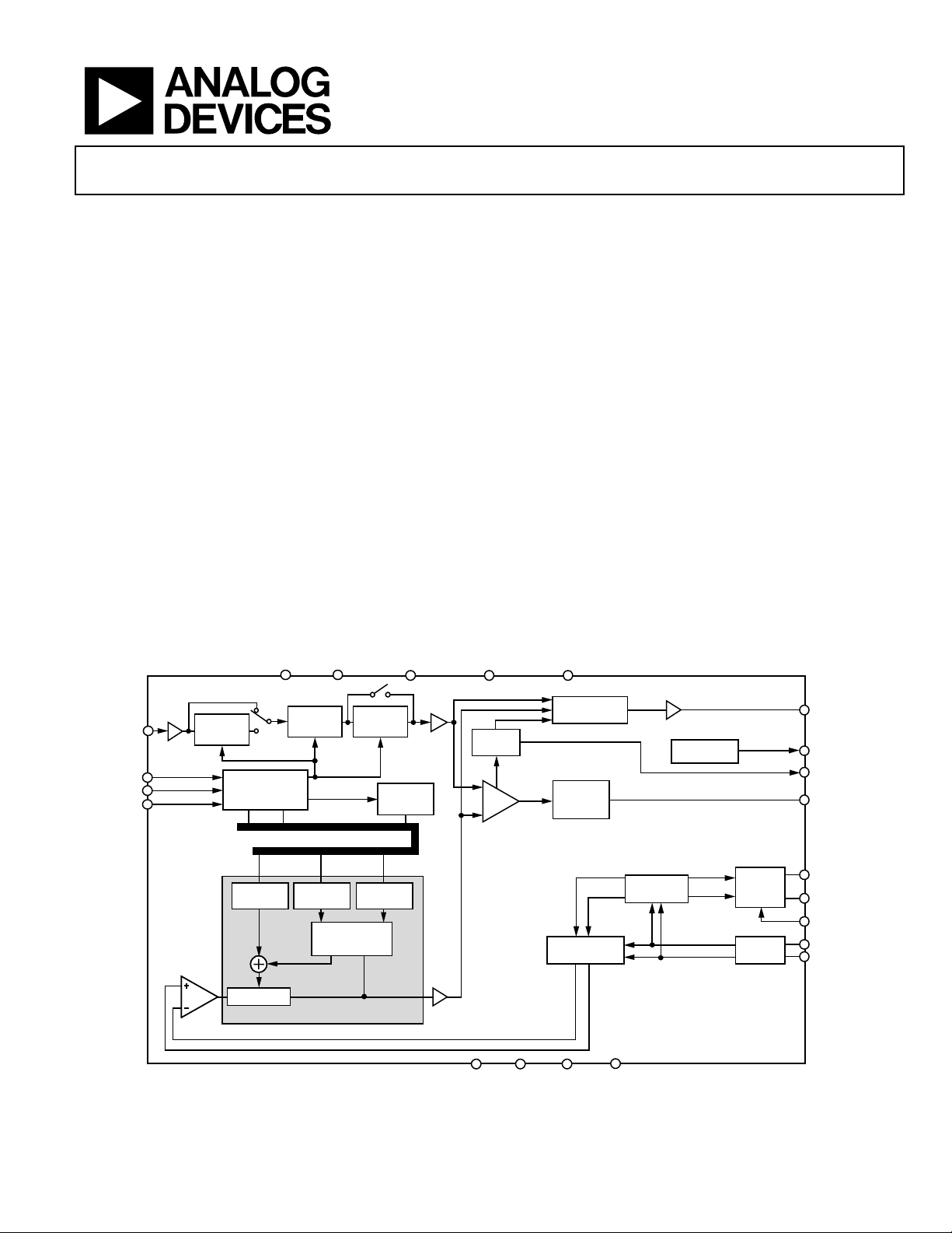
ADF4150
MUXOUT
CP
OUT
LD
SW
REF
IN
CLK
DATA
LE
AV
DD
SDV
DD
DV
DD
V
P
A
GND
CE CP
GND
SD
GND
R
SET
RF
OUT
+
RF
OUT
–
RF
IN
+
RF
IN
–
PHASE
COMPARATOR
FL
O
SWITCH
CHARGE
PUMP
OUTPUT
STAGE
RF
INPUT
PDB
RF
MULTIPLEXER
10-BIT R
COUNTER
÷2
DIVIDER
×2
DOUBLER
FUNCTION
LATCH
DATA REGIS TER
INTEGER
REG
N COUNTER
FRACTION
REG
THIRD-ORDER
FRACTIONAL
INTERPOLATOR
MODULUS
REG
MULTIPLEXER
LOCK
DETECT
ADF4150
08226-001
DIVIDE-BY-1/
-2/-4/-8/-16
Fractional-N/Integer-N PLL Synthesizer
FEATURES
Fractional-N synthesizer and integer-N synthesizer
Programmable divide-by-1/-2/-4/-8/-16 output
5.0 GHz RF bandwidth
3.0 V to 3.6 V power supply
1.8 V logic compatibility
Separate charge pump supply (V
voltage in 3 V systems
Programmable dual-modulus prescaler of 4/5 or 8/9
Programmable output power level
RF output mute function
3-wire serial interface
Analog and digital lock detect
Switched bandwidth fast-lock mode
Cycle slip reduction
APPLICATIONS
Wireless infrastructure (W-CDMA, TD-SCDMA, WiMax, GSM,
PCS, DCS, DECT)
Test equipment
Wireless LANs, CATV equipment
Clock generation
) allows extended tuning
P
GENERAL DESCRIPTION
The ADF4150 allows implementation of fractional-N or
integer-N phase-locked loop (PLL) frequency synthesizers
if used with an external voltage-controlled oscillator (VCO),
loop filter, and external reference frequency.
The ADF4150 is for use with external VCO parts and is
software compatible with the ADF4350. The VCO frequency
can be divided by 1/2/4/8/16 to allow the user to generate RF
output frequencies as low as 31.25 MHz. For applications that
require isolation the RF output stage can be muted. The mute
function is both pin and software controllable.
Control of all the on-chip registers is through a simple 3-wire
interface. The device operates with a power supply ranging
from 3.0 V to 3.6 V and can be powered down when not in use.
The ADF4150 is available in a 4 mm × 4 mm package.
FUNCTIONAL BLOCK DIAGRAM
Rev. 0
Information furnished by Analog Devices is believed to be accurate and reliable. However, no
responsibility is assumed by Analog Devices for its use, nor for any infringements of patents or other
rights of thi rd parties that may result from its use. Specifications subject to change with out notice. No
license is granted by implication or otherwise under any patent or patent rights of Analog Devices.
Trademarks and registered trademarks are the property of their respective owners.
Figure 1.
One Technology Way, P.O. Box 9106, Norwood, MA 02062-9106, U.S.A.
Tel: 781.329.4700
Fax: 781.461.3113 ©2011 Analog Devices, Inc. All rights reserved.
www.analog.com

ADF4150
TABLE OF CONTENTS
Features .............................................................................................. 1
Applications ....................................................................................... 1
General Description ......................................................................... 1
Functional Block Diagram .............................................................. 1
Revision History ............................................................................... 2
Specifications ..................................................................................... 3
Timing Characteristics ................................................................ 5
Absolute Maximum Ratings ............................................................ 6
Transistor Count ........................................................................... 6
ESD Caution .................................................................................. 6
Pin Configuration and Function Descriptions ............................. 7
Typical Performance Characteristics ............................................. 9
Circuit Description ......................................................................... 11
Reference Input Section ............................................................. 11
RF N Divider ............................................................................... 11
INT, FRAC, MOD, and R Counter Relationship.................... 11
INT N Mode ................................................................................ 11
R Counter .................................................................................... 11
Phase Frequency Detector (PFD) and Charge Pump ............ 11
MUXOUT and Lock Detect ...................................................... 12
Input Shift Registers ................................................................... 12
Program Modes .......................................................................... 12
Output Stage ................................................................................ 12
Register Maps .................................................................................. 13
Register 0 ..................................................................................... 18
Register 1 ..................................................................................... 18
Register 2 ..................................................................................... 18
Register 3 ..................................................................................... 20
Register 4 ..................................................................................... 20
Register 5 ..................................................................................... 20
Initialization Sequence .............................................................. 20
RF Synthesizer—A Worked Example ...................................... 21
Modulus ....................................................................................... 21
Reference Doubler and Reference Divider ............................. 21
12-Bit Programmable Modulus ................................................ 21
Cycle Slip Reduction for Faster Lock Times ........................... 22
Spurious Optimization and Fast lock ...................................... 22
Fast Lock Timer and Register Sequences ................................ 22
Fast Lock—An Example ............................................................ 23
Fast Lock—Loop Filter Topology ............................................. 23
Spur Mechanisms ....................................................................... 23
Spur Consistency and Fractional Spur Optimization ........... 24
Phase Resync ............................................................................... 24
Applications Information .............................................................. 25
Direct Conversion Modulator .................................................. 25
Interfacing ................................................................................... 26
PCB Design Guidelines for Chip Scale Package .................... 26
Output Matching ........................................................................ 27
Outline Dimensions ....................................................................... 28
Ordering Guide .......................................................................... 28
REVISION HISTORY
7/11—Revision 0: Initial Version
Rev. 0 | Page 2 of 28

ADF4150
INL
SPECIFICATIONS
AVDD = DVDD = SD
operating temperature range is −40°C to +85°C.
Table 1.
Parameter
REFIN CHARACTERISTICS
Input Frequency 10 250 MHz For f < 10 MHz ensure slew rate > 21 V/µs
Input Sensitivity 0.7 AVDD V p-p Biased at AVDD/21
Input Capacitance 5.0 pF
Input Current ±60 µA
RF INPUT CHARACTERISTICS
RF Input Frequency (RFIN), RF Output
Buffer Disabled
RF Input Frequency (RFIN), RF Output
Buffer Disabled
RF Input Frequency (RFIN) RF Output
Buffer Enabled
RF Input Frequency (RFIN) RF Output
Buffer and Dividers Enabled
Prescaler Output Frequency 750 MHz
MAXIMUM PFD FREQUENCY
Fractional-N (Low Spur Mode) 26 MHz
Fractional-N Mode (Low Noise Mode) 32 MHz
Integer-N Mode 32 MHz
CHARGE PUMP
ICP Sink/Source R
High Value 4.65 mA
Low Value 0.29 mA
R
Range 2.7 10 kΩ
SET
I
Leakage 1 nA VCP = VP/2
CP
Sink and Source Current Matching 2 % 0.5 V ≤ VCP ≤ VP − 0.5 V
ICP vs. VCP 1 % 0.5 V ≤ VCP ≤ VP − 0.5 V
ICP vs. Temperature 2 % VCP = VP/2
LOGIC INPUTS
Input High Voltage, V
Input Low Voltage, V
Input Current, I
Input Capacitance, CIN 3.0 pF
LOGIC OUTPUTS
Output High Voltage, VOH DVDD − 0.4 V CMOS output chosen
Output High Current, IOH 500 µA
Output Low Voltage, VO 0.4 V IOL = 500 µA
POWER SUPPLIES
AVDD 3.0 3.6 V
DVDD, SD
AVDD
VDD
VP AVDD 5.5 V
DIDD + AI
2
50 60 mA
DD
Output Dividers 6 to 24 mA Each output divide by two consumes 6 mA
2
I
24 32 mA RF output stage is programmable
RFOUT
Low Power Sleep Mode 1 µA
= 3.3 V ± 10%; VP = AVDD to 5.5 V; AGND = DGND = 0 V; TA = T
VDD
B Version
Unit Conditions/Comments Min Typ Max
0.5 4.0 GHz −10 dBm ≤ RF input power ≤ +5 dBm
0.5 5.0 GHz −5 dBm ≤ RF input power ≤ +5 dBm
0.5 3.5 GHz −10 dBm ≤ RF input power ≤ +5 dBm
0.5 3.0 GHz −10 dBm ≤ RF input power ≤ +5 dBm
1.5 V
INH
0.6 V
±1 µA
INH/IINL
MIN
to T
SET
, unless otherwise noted. The
MAX
= 5.1 kΩ
Rev. 0 | Page 3 of 28

ADF4150
B Version
Parameter
RF OUTPUT CHARACTERISTICS
Minimum Output Frequency Using RF
31.25 MHz 500 MHz VCO input and divide-by-16 selected
Output Dividers
Maximum RFIN Frequency Using RF
4400 MHz
Output Dividers
Harmonic Content (Second) −19 dBc Fundamental VCO output
Harmonic Content (Third) −13 dBc Fundamental VCO output
Harmonic Content (Second) −20 dBc Divided VCO output
Harmonic Content (Third) −10 dBc Divided VCO output
Output Power 3 −4 dBm Maximum setting
+5 dBm Minimum setting
Output Power Variation ±1 dB
Level of Signal With RF Mute Enabled −40 dBm
NOISE CHARACTERISTICS
Normalized Phase Noise Floor
(PN
SYNTH
4
)
Normalized 1/f Noise (PN
Normalized Phase Noise Floor
(PN
SYNTH
4
)
Normalized 1/f Noise (PN
Spurious Signals Due to PFD
Frequency
6
)5
1_f
)5
1_f
−223 dBc/Hz
−123
dBc/Hz
−222 dBc/Hz
−119
dBc/Hz
−90 dBc VCO output
−75 dBc RF output buffers
1
AC coupling ensures AVDD/2 bias.
2
TA = 25°C; AVDD = DVDD = 3.3 V; prescaler = 8/9; f
3
Using a tuned load.
4
The synthesizer phase noise floor is estimated by measuring the in-band phase noise at the output of the VCO and subtracting 20 log N (where N is the N divider
value) and 10 log F
5
The PLL phase noise is composed of 1/f (flicker) noise plus the normalized PLL noise floor. The formula for calculating the 1/f noise contribution at an RF frequency (FRF)
and at a frequ ency offset (f) is given by PN = P
6
Spurious measured on EVAL-ADF4150EB1Z, using a Rohde & Schwarz FSUP signal source analyzer.
. PN
= PN
PFD
SYNTH
− 10logF
TOT
= 100 MHz; f
REFIN
− 20logN.
PFD
+ 10log(10 kHz/f) + 20log(FRF/1 GHz). Both the normalized phase noise floor and flicker noise are modeled in ADIsimPLL.
1_f
= 26 MHz; fRF = 1.7422 GHz.
PFD
Unit Conditions/Comments Min Typ Max
PLL loop BW = 500 kHz (ABP = 3 ns)
10 kHz offset. Normalized to 1 GHz. (ABP = 3 ns)
PLL loop BW = 500 kHz (ABP = 6 ns); low noise
mode selected
10 kHz offset; normalized to 1 GHz; (ABP = 6 ns);
low noise mode selected
Rev. 0 | Page 4 of 28
ADF4150
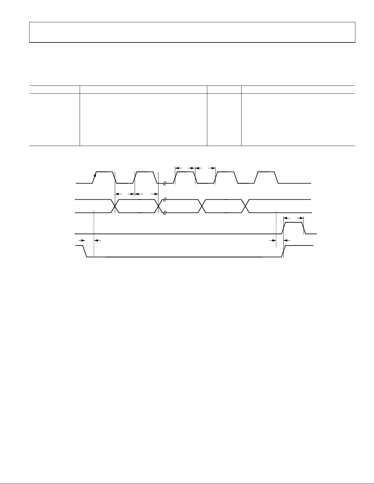
CLK
DATA
LE
LE
DB31 (MSB) DB30
DB1
(CONTROL BIT C2)
DB2
(CONTROL BIT C3)
DB0 (LSB)
(CONTROL BIT C1)
t
1
t
2
t
3
t
7
t
6
t
4
t
5
08226-002
TIMING CHARACTERISTICS
AVDD = DVDD = SD
temperature range is −40°C to +85°C.
Table 2.
Parameter Limit (B Version) Unit Test Conditions/Comments
t1 20 ns min LE setup time
t2 10 ns min DATA to CLK setup time
t3 10 ns min DATA to CLK hold time
t4 25 ns min CLK high duration
t5 25 ns min CLK low duration
t6 10 ns min CLK to LE setup time
t7 20 ns min LE pulse width
= 3.3 V ± 10%; VP = AVDD to 5.5 V; AGND = DGND = 0 V; TA = T
VDD
MIN
to T
, unless otherwise noted. Operating
MAX
Figure 2. Timing Diagram
Rev. 0 | Page 5 of 28
ADF4150
ABSOLUTE MAXIMUM RATINGS
TA = 25°C, unless otherwise noted.
Table 3.
Parameter Rating
AVDD to GND1 −0.3 V to +3.9 V
AVDD to DVDD −0.3 V to +0.3 V
VP to AVDD −0.3 V to +5.8 V
Digital I/O Voltage to GND1 −0.3 V to VDD + 0.3 V
Analog I/O Voltage to GND1 −0.3 V to VDD + 0.3 V
REFIN to GND1 −0.3 V to VDD + 0.3 V
Operating Temperature Range −40°C to +85°C
Storage Temperature Range −65°C to +125°C
Maximum Junction Temperature 150°C
LFCSP θJA Thermal Impedance
(Paddle-Soldered) 27.3°C/W
Reflow Soldering
Peak Temperature 260°C
Time at Peak Temperature 40 sec
1
GND = AGND = DGND = 0 V.
Stresses above those listed under Absolute Maximum Ratings
may cause permanent damage to the device. This is a stress
rating only; functional operation of the device at these or any
other conditions above those indicated in the operational
section of this specification is not implied. Exposure to absolute
maximum rating conditions for extended periods may affect
device reliability.
TRANSISTOR COUNT
23380 (CMOS) and 809 (bipolar)
ESD CAUTION
Rev. 0 | Page 6 of 28

ADF4150
A
GND
AV
DD
2
DV
DD
REF
IN
SDV
DD
SD
GND
MUXOUT
R
SET
RF
OUT
+
RF
OUT
−
PDB
RF
LD
NOTES
1. THE LFCSP HAS AN EXPO S E D P ADDLE
THAT MUST BE CONNECTED TO GND.
PIN 1
INDICATOR
1CLK
2DATA
3LE
4CE
5SW
6V
P
15
16
17
18
14
13
7CP
OUT
8
CP
GND
9
AV
DD
1
11
RF
IN
–
12A
GND
10
RF
IN
+
21
22
23
24
20
19
ADF4150
TOP VIEW
(Not to S cale)
08226-003
Multiplexer Output. This multiplexer output allows either the lock detect, the scaled RF, or the scaled reference
PIN CONFIGURATION AND FUNCTION DESCRIPTIONS
Figure 3. Pin Configuration
Table 4. Pin Function Descriptions
Pin No. Mnemonic Description
1 CLK Serial Clock Input. Data is clocked into the 32-bit shift register on the CLK rising edge. This input is a high
impedance CMOS input.
2 DATA Serial Data Input. The serial data is loaded MSB first with the three LSBs as the control bits. This input is a high
impedance CMOS input.
3 LE Load Enable, CMOS Input. When LE goes high, the data stored in the shift register is loaded into the register
that is selected by the three LSBs.
4 CE Chip Enable. A logic low on this pin powers down the device and puts the charge pump into three-state
mode. Taking the pin high powers up the device depending on the status of the power-down bits.
5 SW Fastlock Switch. Make a connection to this pin from the loop filter when using the fastlock mode.
6 VP Charge Pump Power Supply. This pin should be greater than or equal to AVDD. In systems where AVDD is 3 V, it
can be set to 5.5 V and used to drive a VCO with a tuning range of up to 5.5 V.
7 CP
8 CP
9 AVDD1 Analog Power Supply. This pin ranges from 3.0 V to 3.6 V. Decoupling capacitors to the analog ground plane
10 RFIN+ Input to the RF Input. This small signal input is ac-coupled to the external VCO.
11 RFIN− Complementary Input to the RF Input. This point must be decoupled to the ground plane with a small bypass
12, 13 A
14 RF
15 RF
16 AVDD2 Analog Power Supply. This pin ranges from 3.0 V to 3.6 V. Decoupling capacitors to the analog ground plane
17 PDBRF RF Power-Down. A logic low on this pin mutes the RF outputs. This function is also software controllable.
18 DVDD Digital Power Supply. This pin should be the same voltage as AVDD. Place decoupling capacitors to the ground
19 REFIN Reference Input. This is a CMOS input with a nominal threshold of VDD/2 and a dc equivalent input resistance
20 LD Lock Detect Output Pin. This pin outputs a logic high to indicate PLL lock; a logic low output indicates loss of
21 MUXOUT
Charge Pump Output. When enabled, this provides ±ICP to the external loop filter. The output of the loop filter
OUT
is connected to V
Charge Pump Ground. This is the ground return pin for CP
GND
are to be placed as close as possible to this pin. AV
to drive the external VCO.
TUNE
.
OUT
must have the same value as DVDD.
DD
capacitor, typically 100 pF.
Analog Ground. This is a ground return pin for AVDD1 and AVDD2.
GND
− Complementary RF Output. The output level is programmable. The VCO fundamental output or a divided
OUT
down version is available.
+ RF Output. The output level is programmable. The VCO fundamental output or a divided down version is
OUT
available.
are to be placed as close as possible to this pin. AV
2 must have the same value as DVDD.
DD
plane as close as possible to this pin.
of 100 kΩ. This input can be driven from a TTL or CMOS crystal oscillator, or it can be ac-coupled.
PLL lock.
frequency to be accessed externally.
Rev. 0 | Page 7 of 28

ADF4150
SET
CP
R
I
23.9
=
Pin No. Mnemonic Description
22 SDVDD Power Supply Pin for the Digital Sigma-Delta (Σ-Δ) Modulator. This pin should be the same voltage as AVDD.
Decoupling capacitors to the ground plane are to be placed as close as possible to this pin.
23 SD
24 R
25 EP The exposed pad must be connected to GND.
Digital Σ-Δ Modulator Ground. Ground return path for the Σ-Δ modulator.
GND
Connecting a resistor between this pin and GND sets the charge pump output current. The nominal voltage
SET
bias at the R
pin is 0.48 V. The relationship between ICP and R
SET
SET
is
where:
R
= 5.1 kΩ.
SET
= 5 mA.
I
CP
Rev. 0 | Page 8 of 28
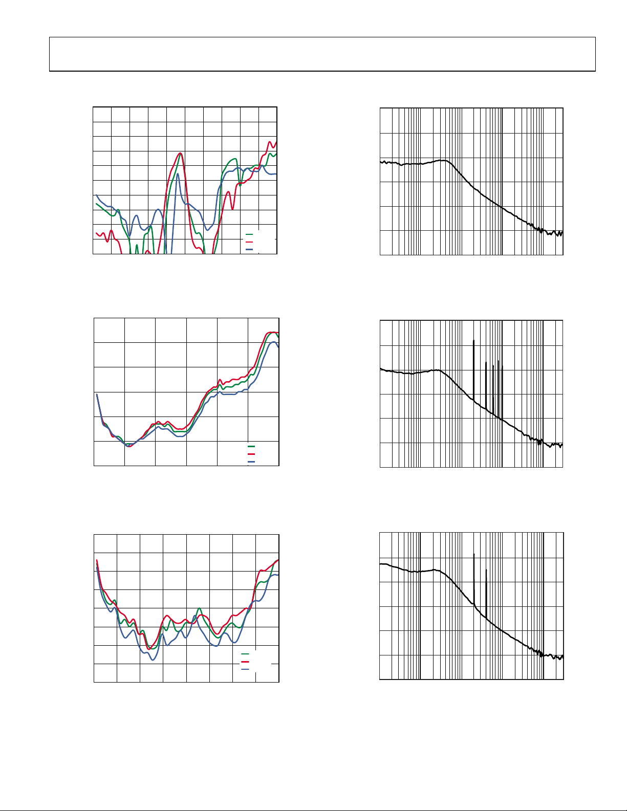
ADF4150
0
–50
0 5.0
POWER (dBm)
FREQUENCY ( GHz)
08226-042
–45
–40
–35
–30
–25
–20
–15
–10
–5
0.5 1.0 1.5 2.0 2.5 3.0 3.5 4.0 4.5
+25°C
+85°C
–40°C
10
–50
0 6
POWER (dBm)
FREQUENCY (MHz)
08226-043
–40
–30
–20
–10
0
1 2 3 4 5
+25°C
+85°C
–40°C
0
–40
0 4.0
POWER (dBm)
FREQUENCY ( GHz)
08226-044
–35
–30
–25
–20
–15
–10
–5
0.5 1.0 1.5 2.0 3.02.5 3.5
+25°C
+85°C
–40°C
–180
–160
–140
–120
–100
–80
–60
POWER (dBc)
08226-045
1k 10k 100k 1M 10M
FREQUENCY (Hz)
1M 10M 100M 1G 10G
FREQUENCY (Hz)
–180
–160
–140
–120
–100
–80
–60
POWER (dBc)
08226-046
1k 10k 100k 1M 10M
FREQUENCY (Hz)
–180
–160
–140
–120
–100
–80
–60
POWER (dBc)
08226-047
TYPICAL PERFORMANCE CHARACTERISTICS
Figure 4. RF Input Sensitivity; RF Output Enabled; Output Divide-by-1
Selected
Figure 5. RF Input Sensitivity; RF Output Disabled
Figure 7. Integer-N Phase Noise and Spur Performance; Low Noise Mode;
VCOOUT = 1750 MHz, REF
= 100 MHz, PFD = 25 MHz, Loop Filter
IN
Bandwidth= 50 kHz
Figure 8. Fractional-N Phase Noise and Spur Performance; Low Noise Mode;
VCOOUT = 1750 MHz, REF
Bandwidth= 15 kHz, Channel Spacing = 200 kHz. FRAC = 26, MOD = 125
= 100 MHz, PFD = 25 MHz, Loop Filter
IN
Figure 6. RF Sensitivity; RF Output Enabled (RF Dividers-by-2/-4/-8/-16
Enabled)
Figure 9. Fractional-N Phase Noise and Spur Performance; Low Spur Mode;
VCOOUT = 1750 MHz, REF
Bandwidth= 50 kHz, Channel Spacing = 200 kHz. FRAC = 26, MOD = 125
= 100 MHz, PFD = 25 MHz, Loop Filter
IN
Rev. 0 | Page 9 of 28

ADF4150
–180
–160
–140
–120
–100
–80
–60
1k 10k 100k 1M 10M
POWER (dBc)
FREQUENCY (Hz)
08226-038
1k 10k 100k 1M 10M
FREQUENCY (Hz)
–180
–160
–140
–120
–100
–80
–60
POWER (dBc)
08226-039
1k 10k 100k 1M 10M
FREQUENCY (Hz)
–180
–160
–140
–120
–100
–80
–60
POWER (dBc)
08226-040
1k 10k 100k 1M 10M
FREQUENCY (Hz)
–180
–160
–140
–120
–100
–80
–60
POWER (dBc)
08226-041
Figure 10. RF Output Phase Noise RF Dividers Used; Integer-N; Low Noise
Mode; VCOOUT = 1750 MHz, REF
= 100 MHz, PFD = 25 MHz, Loop Filter
IN
Bandwidth = 50 kHz
Figure 11. RF Buffer Output Fractional-N Phase Noise and Spur Performance;
Low Noise Mode; VCOOUT = 1750 MHz, REF
Loop Filter Bandwidth = 15 kHz, Channel Spacing = 200 kHz; FRAC = 1,
= 100 MHz, PFD = 25 MHz,
IN
MOD = 5; Output Divider = 1
Figure 12. RF Buffer Output Fractional-N Phase Noise and Spur Performance;
Low Noise Mode; VCOOUT = 1750 MHz, REF
Loop Filter Bandwidth = 15 kHz, Channel Spacing = 200 kHz; FRAC = 1,
= 100 MHz, PFD = 25 MHz,
IN
MOD = 5; Output Divider = 2
Figure 13. RF Buffer Output Fractional-N Phase Noise and Spur Performance;
Low Noise Mode; VCOOUT = 1750 MHz, REF
Loop Filter Bandwidth = 15 kHz, Channel Spacing = 200 kHz. FRAC = 1,
= 100 MHz, PFD = 25 MHz,
IN
MOD = 5. Output divider = 4
Rev. 0 | Page 10 of 28

ADF4150
BUFFER
TO R COUNTER
REF
IN
100kΩ
NC
SW2
SW3
NO
NC
SW1
POWER-DOWN
CONTROL
08226-010
THIRD ORDER
FRACTIONAL
INTERPOLATOR
FRAC
VALUE
MOD
REG
INT
REG
RF N DIVIDE R
N = INT + FRAC/MOD
FROM
VCO OUTPUT/
OUTPUT DIVIDERS
TO PFD
N COUNTER
08226-011
U3
CLR2
Q2D2
U2
DOWN
UP
HIGH
HIGH
CP
–IN
+IN
CHARGE
PUMP
DELAY
CLR1
Q1D1
U1
08226-012
CIRCUIT DESCRIPTION
REFERENCE INPUT SECTION
The reference input stage is shown in Figure 14. SW1 and SW2
are normally closed switches. SW3 is normally open. When
power-down is initiated, SW3 is closed and SW1 and SW2 are
opened. This ensures that there is no loading of the REF
on power-down.
IN
pin
Figure 14. Reference Input Stage
RF N DIVIDER
The RF N divider allows a division ratio in the PLL feedback
path. Division ratio is determined by INT, F RAC , and MOD
values, which build up this divider.
INT, FRAC, MOD, AND R COUNTER RELATIONSHIP
The INT, FRAC, and MOD values, in conjunction with the R
counter, make it possible to generate output frequencies that
are spaced by fractions of the PFD frequency. See the RF
Synthesizer—A Worked Example section for more information. The RF VCO frequency (RF
= f
RF
OUT
× (INT + (FR AC/MOD)) (1)
PFD
where:
RF
is the output frequency of external voltage controlled
OUT
oscillator (VCO).
INT is the preset divide ratio of the binary 16–bit counter
(23 to 65535 for 4/5 prescaler, 75 to 65535 for 8/9 prescaler).
MOD is the preset fractional modulus (2 to 4095).
FRAC is the numerator of the fractional division (0 to MOD − 1).
f
= REFIN × [(1 + D)/(R × (1 + T))] (2)
PFD
where:
REF
is the reference input frequency.
IN
D is the REF
T is the REF
doubler bit.
IN
divide-by-2 bit (0 or 1).
IN
R is the preset divide ratio of the binary 10-bit programmable
reference counter (1 to 1023).
) equation is
OUT
Figure 15. RF INT Divider
INT N MODE
If the FRAC = 0 and DB8 in Register 2 (LDF) is set to 1, the
synthesizer operates in integer-N mode. The DB8 in Register 2
(LDF) should be set to 1 to get integer-N digital lock detect.
Additionally, lower phase noise is possible if the anti-backlash
pulse width is reduced to 3 ns. This mode is not valid for
fractional-N applications.
R COUNTER
The 10–bit R counter allows the input reference frequency
(REF
) to be divided down to produce the reference clock
IN
to the PFD. Division ratios from 1 to 1023 are allowed.
PHASE FREQUENCY DETECTOR (PFD) AND CHARGE PUMP
The phase frequency detector (PFD) takes inputs from the R
counter and N counter and produces an output proportional to
the phase and frequency difference between them. Figure 16 is
a simplified schematic of the phase frequency detector. The
PFD includes a programmable delay element that sets the width
of the antibacklash pulse, which can be either 6 ns (default, for
fractional-N applications) or 3 ns (for integer-N mode). This
pulse ensures there is no dead zone in the PFD transfer function,
and gives a consistent reference spur level.
Figure 16. PFD Simplified Schematic
Rev. 0 | Page 11 of 28

ADF4150
D
GND
DV
DD
CONTROL
MUX
MUXOUT
ANALOG L OCK DETECT
DIGITAL LOCK DETECT
R COUNTER OUTPUT
N COUNTER OUTPUT
DGND
RESERVED
THREE-STATE-OUTPUT
DV
DD
R COUNTER INP UT
08226-013
VCO
RF
OUT
+ RF
OUT
–
BUFFER/
DIVIDE-BY-1/
-2/-4/-8/-16
08226-014
MUXOUT AND LOCK DETECT
The output multiplexer on the ADF4150 allows the user
to access various internal points on the chip. The state of
MUXOUT is controlled by M3, M2, and M1 (for details, see
Figure 22). Figure 17 shows the MUXOUT section in block
diagram form.
INPUT SHIFT REGISTERS
The ADF4150 digital section includes a 10-bit RF R counter,
a 16-bit RF N counter, a 12-bit FRAC counter, and a 12-bit
modulus counter. Data is clocked into the 32-bit shift register
on each rising edge of CLK. The data is clocked in MSB first.
Data is transferred from the shift register to one of six latches
on the rising edge of LE. The destination latch is determined
by the state of the three control bits (C3, C2, and C1) in the
shift register. These are the 3 LSBs, DB2, DB1, and DB0, as
shown in Figure 2. The truth table for these bits is shown in
Table 5. Figure 19 shows a summary of how the latches are
programmed.
Table 5. C3, C2, and C1 Truth Table
C3 C2 C1 Register
0 0 0 Register 0 (R0)
0 0 1 Register 1 (R1)
0 1 0 Register 2 (R2)
0 1 1 Register 3 (R3)
1 0 0 Register 4 (R4)
1 0 1 Register 5 (R5)
Figure 17. MUXOUT Schematic
Control Bits
PROGRAM MODES
Figure 20 through Figure 25 show how the program modes are
to be set up in the ADF4150.
A number of settings in the ADF4150 are double buffered.
These include the modulus value, phase value, R counter
value, reference doubler, reference divide-by-2, and current
setting. This means that two events have to occur before the
part uses a new value of any of the double-buffered settings.
First, the new value is latched into the device by writing to the
appropriate register. Second, a new write must be performed
on Register R0. For example, any time the modulus value is
updated, Register R0 must be written to, thus ensuring the
modulus value is loaded correctly. Divider select in Register 4
(R4) is also double buffered, but only if DB13 of Register 2 (R2)
is high.
OUTPUT STAGE
The RF
to the collectors of an NPN differential pair driven by buffered
outputs of the VCO, as shown in Figure 18. To allow the user
to optimize the power dissipation vs. the output power requirements, the tail current of the differential pair is programmable
by Bit D2 and Bit D1 in Register 4 (R4). Four current levels may
be set. These levels give output power levels of −4 dBm, −1 dBm,
+2 dBm, and +5 dBm, respectively, using a 50 Ω resistor to
AV
outputs can be combined in a 1 + 1:1 transformer or a 180°
microstrip coupler (see the Output Matching section). If the
outputs are used individually, the optimum output stage
consists of a shunt inductor to AV
Another feature of the ADF4150 is that the supply current
to the RF output stage can be shut down until the part
achieves lock as measured by the digital lock detect circuitry.
This is enabled by the mute-till-lock detect (MTLD) bit in
Register 4 (R4).
Rev. 0 | Page 12 of 28
+ and RF
OUT
and ac coupling into a 50 Ω load. Alternatively, both
DD
− pins of the ADF4150 are connected
OUT
.
DD
Figure 18. Output Stage

ADF4150
DB31
DB30 DB29 DB28 DB27 DB26 DB25 DB24 DB23 DB22 DB21 DB20 DB19 DB18 DB17 DB16 DB15
DB14 DB13 DB12 DB11 DB10 DB9 DB8 DB7 DB6 DB5 DB4 DB3 DB2 DB1 DB0
0
N16 N15 N14 N13 N12 N11 N10 N9
RESERVED
16-BIT INTEGER VALUE ( INT) 12-BIT F RACTIONAL VALUE ( FRAC)
CONTROL
BITS
N8 N7 N6 N5 N4 N3 N2 N1 F12 F11 F10 F9 F8 F7 F6 F5 F4 F3 F2 F1 C3(0) C2(0)
C1(0)
DB31 DB30 DB29 DB28 DB27 DB26 DB25 DB24 DB23 DB22 DB21 DB20 DB19 DB18
DB17 DB16 DB15 DB14 DB13 DB12 DB11 DB10 DB9 DB8 DB7 DB6 DB5 DB4 DB3 DB2 DB1 DB0
0 0 0 0 PR1 P12 P11 P10 P9
12-BIT PHASE VALUE (PHASE)
12-BIT MODULUS VALUE ( MOD)
CONTROL
BITS
P8 P7 P6 P5 P4 P3 P2 P1 M12 M11 M10 M9 M8 M7 M6 M5 M4 M3 M2 M1
C3(0) C2(0) C1(1)
DB31 DB30 DB29 DB28 DB27 DB26 DB25 DB24 DB23 DB22 DB21
DB20 DB19 DB18 DB17 DB16 DB15 DB14 DB13 DB12 DB11 DB10 DB9 DB8 DB7 DB6 DB5 DB4 DB3 DB2 DB1 DB0
0 L2 L1 M3 M2 M1 RD2 RD1 R10 R9 R8 R7 R6 R5 R4 R3 R2 R1 D1 CP4 CP3 CP2 CP1 U6 U5 U4 U3 U2 U1 C3(0) C2(1)
C1(0)
CSR
RDIV2
REFERENCE
DOUBLER
CHARGE
PUMP
CURRENT
SETTING
10-BIT R COUNTER
CONTROL
BITS
DB31 DB30
DB29 DB28 DB27 DB26 DB25 DB24 DB23 DB22 DB21 DB20 DB19 DB18 DB17 DB16 DB15 DB14 DB13 DB12 DB11 DB10 DB9 DB8 DB7 DB6 DB5 DB4 DB3 DB2 DB1 DB0
0 0 0 0 0 0 0 0 0 F3 F2 0 0 F1 0 C2 C1 D12 D11 D10 D9
D8 D7 D6 D5 D4 D3 D2 D1 C3(0) C2(1) C1(1)
CONTROL
BITS
12-BIT CL OCK DIVIDER VALUE
LDP
PD
POLARITY
POWER-DOWN
CP THREE-
STATE
COUNTER
RESET
OUTPUT
POWER
CLK
DIV
MODE
DBR
1
1
DBR = DOUBLE BUFFERED REGI S TER—BUFFERE D BY THE WRIT E TO REGIS TER 0.
2
DBB = DOUBLE BUFFERED BITS — BUFFERED BY THE WRITE T O REGIST E R 0, IF AND ONLY IF DB13 OF REGIST E R 2 IS HIGH.
RESERVED
LDF
RESERVED
ABP
CHARGE
CANCEL
RESERVED
REGISTER 4
DB31 DB30 DB29 DB28 DB27 DB26 DB25 DB24 DB23 DB22 DB21 DB20 DB19 DB18 DB17 DB16 DB15 DB14 DB13 DB12 DB11 DB10 DB9 DB8 DB7 DB6 DB5 DB4 DB3 DB2 DB1 DB0
0 0 0 0 0 0 0 0 D13 D12 D11 D10 BS8 BS7 BS6 BS5 BS4 BS3 BS2 BS1 D9 D8 D7 D6 D5 D4 D3 D2 D1 C3(1) C2(0) C1(0)
CONTROL
BITS
RESERVED RESERVED
RF OUTPUT
ENABLE
LD PIN
MODE
MTLD
DIVIDER
SELECT
FEEDBACK
SELECT
REGISTER 0
REGISTER 1
REGISTER 2
REGISTER 3
REGISTER 5
DB31 DB30 DB29 DB28 DB27 DB26 DB25 DB24 DB23 DB22 DB21 DB20 DB19 DB18 DB17 DB16 DB15 DB14 DB13 DB12 DB11 DB10 DB9 DB8 DB7 DB6 DB5 DB4 DB3 DB2 DB1 DB0
0 0 0 0 0 0 0 0 D15 D14 0 1 1 0 0 0 0 0 0 0 0 0 0 0 0 0 0 0 0 C3(1) C2(0) C1(1)
CONTROL
BITS
RESERVED
RESERVED
DBB
2
DOUBLE BUFF
RESERVED
RESERVED
DBR
1
DBR
1
DBR
1
DBR
1
DBR
1
RESERVED
RESERVED
RESERVED
PRESCALER
LOW
NOISE AND
LOW SPUR
MODES
MUXOUT
08226-015
REGISTER MAPS
Figure 19. Register Summary
Rev. 0 | Page 13 of 28

ADF4150
N16 N15 ... N5 N4 N3 N2 N1 INTEGER VALUE (I NT )
0 0 ... 0 0 0 0 0 NOT ALLOWED
0 0 ... 0 0 0 0 1 NOT ALLOWED
0 0 ... 0 0 0 1 0 NOT ALLOWED
. . ... . . . . . ...
0 0 ... 1 0 1 1 0 NOT ALLOWED
0 0 ... 1 0 1 1 1 23
0 0 ... 1 1 0 0 0 24
. . ... . . . . . ...
1 1 ... 1 1 1 0 1 65533
1 1 ... 1 1 1 1 0 65534
1 1 ... 1 1 1 1 1 65535
F12 F11 .......... F2 F1 FRACTI ONAL VALUE (FRAC)
0 0 .......... 0 0 0
0 0 .......... 0 1 1
0 0 .......... 1 0 2
0 0 .......... 1 1 3
. . .......... . . .
. . .......... . . .
. . .......... . . .
1 1 .......... 0 0 4092
1 1 .......... 0 1 4093
1 1 .......... 1 0 4094
1 1 ......... 1 1 4095
DB31
DB30 DB29 DB28 DB27 DB26 DB25 DB24 DB23 DB22 DB21 DB20 DB19 DB18 DB17 DB16 DB15 DB14 DB13 DB12 DB11 DB10 DB9 DB8 DB7 DB6 DB5 DB4 DB3 DB2 DB1 DB0
0
N16 N15 N14 N13 N12 N11 N10 N9
RESERVED
16-BIT INTEGER VALUE ( INT) 12-BIT F RACTIONAL VALUE ( FRAC)
CONTROL
BITS
N8 N7 N6 N5 N4 N3 N2 N1 F12 F11 F10 F9 F8 F7 F6 F5 F4 F3 F2 F1 C3(0) C2(0) C1(0)
INTmin = 75 wit h prescaler = 8/9
08226-016
P12 P11 .......... P2 P1 PHASE VALUE (PHASE)
0 0 .......... 0 0 0
0 0 .......... 0 1 1 (RECOM M E NDED)
0 0 .......... 1 0 2
0 0 .......... 1 1 3
. . .......... . . .
. . .......... . . .
. . .......... . . .
1 1 .......... 0 0 4092
1 1 .......... 0 1 4093
1 1 .......... 1 0 4094
1 1 .......... 1 1 4095
DB31 DB30 DB29 DB28 DB27 DB26 DB25 DB24 DB23 DB22 DB21 DB20 DB19 DB18 DB17 DB16 DB15 DB14 DB13 DB12 DB11 DB10 DB9 DB8 DB7 DB6 DB5 DB4 DB3 DB2 DB1 DB0
0 0 0 0 PR1 P12 P11 P10 P9
12-BIT PHASE VALUE (PHASE) 12-BIT MODULUS VALUE ( M OD)
CONTROL
BITS
P8 P7 P6 P5 P4 P3 P2 P1 M12 M11 M10 M9 M8 M7 M6 M5 M4 M3 M2 M1 C3(0) C2(0) C1(1)
RESERVED
M12 M11 ..........
..........
..........
..........
..........
..........
..........
..........
..........
..........
M2 M1 INTERPOL ATOR MODULUS (MOD)
0 0 1 0 2
0 0 1 1 3
. . . . .
. . . . .
. . . . .
1 1 0 0 4092
1 1 0 1 4093
1 1 1 0 4094
1 1 1 1 4095
PRESCALER
P1 PRESCALER
0 4/5
1 8/9
DBR DBR
08226-017
Figure 20. Register 0 (R0)
Figure 21. Register 1 (R1)
Rev. 0 | Page 14 of 28

ADF4150
RD2
REFERENCE
DOUBLER
0 DISABLED
1 ENABLED
RD1 REFERENCE DIVIDE BY 2
0 DISABLED
1 ENABLED
CP4 CP3 CP2 CP1
ICP(mA)
4.7kΩ
0 0 0 0 0.31
0 0 0 1 0.63
0 0 1 0 0.94
0 0 1 1 1.25
0 1 0 0 1.56
0 1 0 1 1.88
0 1 1 0 2.19
0 1 1 1 2.50
1 0 0 0 2.81
1 0 0 1 3.13
1 0 1 0 3.44
1 0 1 1 3.75
1 1 0 0 4.06
1 1 0 1 4.38
1 1 1 0 4.69
1 1 1 1 5.00
R10 R9 ..........
..........
..........
..........
..........
..........
..........
..........
..........
..........
R2 R1 R DIVIDER (R)
0 0 0 1 1
0 0 1 0 2
. . . . .
. . . . .
. . . . .
1 1 0 0 1020
1 1 0 1 1021
1 1 1 0 1022
1 1 1 1 1023
DB31 DB30 DB29 DB28 DB27 DB26 DB25 DB24 DB23 DB22 DB21 DB20 DB19 DB18 DB17 DB16 DB15 DB14 DB13 DB12 DB11 DB10 DB9 DB8 DB7 DB6 DB5 DB4 DB3 DB2 DB1 DB0
0 L2 L1 M3 M2 M1 RD2 RD1 R10 R9 R8 R7 R6 R5 R4 R3 R2 R1 D1 CP4 CP3 CP2 CP1 U6 U5 U4 U3 U2 U1 C3(0) C2(1) C1(0)
RDIV2 DBR
REFERENCE
DOUBLER DBR
CHARGE
PUMP
CURRENT
SETTING
10-BIT R COUNTER DBR
CONTROL
BITS
LDP
PD
POLARITY
POWER-DOWN
CP THREE-
STATE
COUNTER
RESET
LDF
MUXOUT
DOUBLE BUFF
U5 LDP
0 10ns
1 6ns
U4 PD POLARITY
0 NEGATIVE
1 POSITIVE
U3 POWER-DOWN
0 DISABLED
1 ENABLED
U2
CP
THREE-STATE
0 DISABLED
1 ENABLED
U1
COUNTER
RESET
0 DISABLED
1 ENABLED
D1
DOUBLE BUFFER
R4 DB22:DB20
0 DISABLED
1 ENABLED
U6 LDF
0 FRAC-N
1 INT-N
RESERVED
M3 M2 M1 OUTPUT
0 0 0 THREE-STATE OUTPUT
0 0 1 DV
DD
0 1 0 DGND
0 1 1 R DIVIDER OUTPUT
1 0 0 N DIVIDER OUTPUT
1 0 1 ANALOG LOCK DETECT
1 1 0 DIGITAL LOCK DETECT
1 1 1 RESERVED
L1 L2 NOISE MODE
0 0 LOW NOISE MODE
0 1 RESERVED
1 0 RESERVED
1 1 LOW SPUR MODE
LOW
NOISE AND
LOW SPUR
MODES
08226-018
Figure 22. Register 2 (R2)
Rev. 0 | Page 15 of 28

ADF4150
C2 C1 CLOCK DIVI DER MODE
0 0 CLO CK DIVIDER OF F
0 1 FAST L OCK ENABLE
1 0 RESYNC ENABLE
1 1 RESERVED
D12 D11 .......... D2 D1 CLOCK DIVIDER VALUE
0 0 .......... 0 0 0
0 0 .......... 0 1 1
0 0 .......... 1 0 2
0 0 .......... 1 1 3
. . .......... . . .
. . .......... . . .
. . .......... . . .
1 1 .......... 0 0 4092
1 1 .......... 0 1 4093
1 1 .......... 1 0 4094
1 1 .......... 1 1 4095
CSR
DB31 DB30 DB29 DB28 DB27 DB26 DB25 DB24 DB23 DB22 DB21 DB20 DB19 DB18 DB17 DB16 DB15 DB14 DB13 DB12 DB11 DB10 DB9 DB8 DB7 DB6 DB5 DB4 DB3 DB2 DB1 DB0
0 0 0 0 0 0 0 0 0 F1 0 C2 C1 D12 D11 D10 D9 D8 D7 D6 D5 D4 D3 D2 D1 C3(0) C2(1) C1(1)
CONTROL
BITS12-BIT CL OCK DIVIDER VALUE
CLK
DIV
MODE
RESERVED
F1
CYCLE SLIP
REDUCTION
0 DISABLED
1 ENABLED
RESERVED
0
0
RESERVED
08226-019
F3 F2
F2
CHARGE
CANCELL
ATION
0 DISABLED
1 ENABLED
F3
ANTIBACKLASH
PULSE WIDTH
0 6ns (FRAC
-N)
1 3ns (INT_N)
CHARGE
CANCEL
ABP
D3 RF OUT
0 DISABLED
1 ENABLED
D2 D1 OUTPUT POWER
0 0 –4
0 1 –1
1 0 +2
1 1 +5
D8
MUTE TILL
LOCK DETECT
0 MUT E DISABLED
1 MUT E ENABL ED
D12 D11 RF DIVIDER SELE CT
0 0 ÷1
0 0 ÷2
0 1 ÷4
0 1 ÷8
D10
0
1
0
1
1 0 ÷160
D13
FEEDBACK
SELECT
0
FUNDAMENTAL
1
DIVIDED
08226-020
OUTPUT
POWER
DB31 DB30 DB29 DB28 DB27 DB26 DB25 DB24 DB23 DB22 DB21 DB20 DB19 DB18 DB17 DB16 DB15 DB14 DB13 DB12 DB11 DB10 DB9 DB8 DB7 DB6 DB5 DB4 DB3 DB2 DB1 DB0
0 0 0 0 0 0 0 0 D13 D12 D11 D10 BS8 BS7 BS6 BS5 BS4 BS3 BS2 BS1 D9 D8 D7 D6 D5 D4 D3 D2 D1 C3(1) C2(0) C1(0)
CONTROL
BITS
RESERVED RESERVED
RF OUTPUT
ENABLE
MTLD
DIVIDER
SELECT
FEEDBACK
SELECT
RESERVED
DBB
2
Figure 23. Register 3 (R3)
Figure 24. Register 4 (R4)
Rev. 0 | Page 16 of 28

ADF4150
LD PIN
MODE
DB31 DB30 DB29 DB28 DB27 DB26 DB25 DB24 DB23 DB22 DB21 DB20 DB19 DB18 DB17 DB16 DB15 DB14 DB13 DB12 DB11 DB10 DB9 DB8 DB7 DB6 DB5 DB4 DB3 DB2 DB1 DB0
0 0 0 0 0 0 0 0 D15 D14 0 0 0 0 0 0 0 0 0 0 0 0 0 0 0 0 0 0 0 C3(1) C2(0) C1(1)
CONTROL
BITSRESERVEDRESERVED
RESERVED
D15 D1 4 LOCK DETECT PIN OPERATION
0 0 LOW
0 1 DIGITAL LOCK DETECT
1 0 LOW
1 1 HIGH
RESERVED
08226-021
Figure 25. Register 5 (R5)
Rev. 0 | Page 17 of 28

ADF4150
REGISTER 0
Control Bits
With Bits[C3:C1] set to 0, 0, 0, Register 0 is programmed.
Figure 20 shows the input data format for programming this
register.
16-Bit Integer Value (INT)
These 16 bits set the INT value, which determines the integer
part of the feedback division factor. They are used in Equation 1
(see the INT, FRAC, MOD, and R Counter Relationship section).
All integer values from 23 to 65,535 are allowed for 4/5 prescaler.
For 8/9 prescaler, the minimum integer value is 75.
12-Bit Fractional Value(FRAC)
The 12 FRAC bits set the numerator of the fraction that is input
to the Σ-Δ modulator. This, along with INT, specifies the new
frequency channel that the synthesizer locks to, as shown in the
RF Synthesizer—A Worked Example section. FRAC values from
0 to MOD − 1 cover channels over a frequency range equal to
the PFD reference frequency.
REGISTER 1
Control Bits
With Bits[C3:C1] set to 0, 0, 1, Register 1 is programmed.
Figure 21 shows the input data format for programming
this register.
Prescaler Value
The dual modulus prescaler (P/P + 1), along with the INT,
FRAC, and MOD counters, determines the overall division
ratio from the VCO output to the PFD input.
Operating at CML levels, it takes the clock from the VCO
output and divides it down for the counters. It is based on a
synchronous 4/5 core. When set to 4/5, the maximum RF
frequency allowed is 3 GHz. Therefore, when operating the
ADF4150 above 3 GHz, this must be set to 8/9. The prescaler
limits the INT value, where:
P = 4/5, N
P = 8/9, N
In the ADF4150, P1 in Register 1 sets the prescaler values.
MIN
MIN
= 23
= 75
12-Bit Phase Value (Phase)
These bits control what is loaded as the phase word. The word
must be less than the MOD value programmed in Register 1.
The word is used to program the RF output phase from 0° to
360° with a resolution of 360°/MOD. See the Phase Resync
section for more information. In most applications, the phase
relationship between the RF signal and the reference is not
important. In such applications, the PHASE value can be used
to optimize the fractional and subfractional spur levels. See the
Spur Consistency and Fractional Spur Optimization section for
more information.
If neither the PHASE resync nor the spurious optimization
functions are being used, it is recommended that the PHASE
word be set to 1.
12-Bit Modulus Value (MOD)
This programmable register sets the fractional modulus. This
is the ratio of the PFD frequency to the channel step resolution
on the RF output. See the RF Synthesizer—A Worked Example
section for more information.
REGISTER 2
Control Bits
With Bits[C3:C1] set to 0, 1, 0, Register 2 is programmed.
Figure 22 shows the input data format for programming
this register.
Low Noise and Spur Modes
The noise modes on the ADF4150 are controlled by DB30 and
DB29 in Register 2 (see
user to optimize a design either for improved spurious performance or for improved phase noise performance.
When the lowest spur setting is chosen, dither is enabled. This
randomizes the fractional quantization noise so it resembles
white noise rather than spurious noise. As a result, the part is
optimized for improved spurious performance. This operation
would normally be used when the PLL closed-loop bandwidth
is wide, for fast-locking applications. (Wide loop bandwidth is
seen as a loop bandwidth greater than 1/10 of the RF
step resolution (f
spurs to the same level as a narrow loop bandwidth.
For best noise performance, use the lowest noise setting option.
As well as disabling the dither, it also ensures that the charge
pump is operating in an optimum region for noise performance.
This setting is extremely useful where a narrow loop filter bandwidth is available. The synthesizer ensures extremely low noise
and the filter attenuates the spurs. The typical performance
characteristics give the user an idea of the trade-off in a typical
W-CDMA setup for the different noise and spur settings.
Figure 22). The noise modes allow the
channel
OUT
)). A wide loop filter does not attenuate the
RES
Rev. 0 | Page 18 of 28

ADF4150
MUXOUT
The on-chip multiplexer is controlled by Bits[DB28:DB26] (see
Figure 22).
Reference Doubler
Setting DB25 to 0 feeds the REFIN signal directly to the 10-bit
R counter, disabling the doubler. Setting this bit to 1 multiplies
the REF
10-bit R counter. When the doubler is disabled, the REF
frequency by a factor of 2 before feeding into the
IN
IN
falling edge is the active edge at the PFD input to the fractional
synthesizer. When the doubler is enabled, both the rising and
falling edges of REF
become active edges at the PFD input.
IN
When the doubler is enabled and the lowest spur mode is
chosen, the in-band phase noise performance is sensitive to the
REF
duty cycle. The phase noise degradation can be as much
IN
as 5 dB for the REF
The phase noise is insensitive to the REF
lowest noise mode. The phase noise is insensitive to the REF
duty cycles outside a 45% to 55% range.
IN
duty cycle in the
IN
IN
duty cycle when the doubler is disabled.
The maximum allowable REF
frequency when the doubler is
IN
enabled is 30 MHz.
RDIV2
Setting the DB24 bit to 1 inserts a divide-by-2 toggle flip-flop
between the R counter and PFD, which extends the maximum
REF
input rate. This function allows a 50% duty cycle signal
IN
to appear at the PFD input, which is necessary for cycle slip
reduction.
10-Bit R Counter
The 10-bit R counter allows the input reference frequency
(REF
) to be divided down to produce the reference clock to
IN
the PFD. Division ratios from 1 to 1023 are allowed.
Double Buffer
DB13 enables or disables double buffering of Bits[DB22:DB20]
in Register 4. The Divider Select section explains how double
buffering works.
Current Setting
Bits[DB12:DB9] set the charge pump current setting. This
should be set to the charge pump current that the loop filter
is designed with (see Figure 22).
LDF
Setting DB8 to 1 enables integer-N digital lock detect, when
the FRAC part of the divider is zero; setting DB8 to 0 enables
fractional-N digital lock detect.
Lock Detect Precision (LDP)
When DB7 is set to 0, the fractional-N digital lock detect is
activated. In this case after setting DB7 to 0, 40 consecutive PFD
cycles of 10 ns must occur before digital lock detect is set. When
DB7 is programmed to 1, 40 consecutive reference cycles of 6 ns
must occur before digital lock detect goes high. Setting DB8 to 1
causes the activation of the integer-N digital lock detect. In this
case, after setting DB7 to 0, 5 consecutive cycles of 10 ns must
occur before digital lock detect is set. When DB7 is set to 1, five
consecutive cycles of 6 ns must occur.
Phase Detector Polarity
DB6 sets the phase detector polarity. When a passive loop filter,
or noninverting active loop filter is used, set this bit to 1. If an
active filter with an inverting characteristic is used, this bit
should be set to 0.
Power-Down (PD)
DB5 provides the programmable power-down mode. Setting this
bit to 1 performs a power-down. Setting this bit to 0 returns the
synthesizer to normal operation. When in software power-down
mode, the part retains all information in its registers. Only if the
supply voltages are removed are the register contents lost.
When a power-down is activated, the following events occur:
• The synthesizer counters are forced to their load state
conditions.
• The charge pump is forced into three-state mode.
• The digital lock detect circuitry is reset.
• The RF
buffers are disabled.
OUT
• The input register remains active and capable of loading
and latching data.
Charge Pump (CP) Three-State
DB4 puts the charge pump into three-state mode when
programmed to 1. It should be set to 0 for normal operation.
Counter Reset
DB3 is the R counter and N counter reset bit for the ADF4150.
When this bit is 1, the RF synthesizer N counter and R counter
are held in reset. For normal operation, this bit should be set to 0.
Rev. 0 | Page 19 of 28

ADF4150
REGISTER 3
Control Bits
With Bits[C3:C1] set to 0, 1, 1, Register 3 is programmed.
Figure 23 shows the input data format for programming
this register.
Antibacklash Pulse Width
Setting DB22 to 0 sets the PFD antibacklash pulse width to 6 ns.
This is the recommended mode for fractional-N use. By setting
this bit to 1, the 3 ns pulse width is used and results in a phase
noise and spur improvement in integer-N operation. For
fractional-N mode it is not recommended to use this smaller
setting.
Charge Cancellation Mode Pulse Width
Setting DB21 to 1 enables charge pump charge cancellation.
This has the effect of reducing PFD spurs in integer-N mode.
In fractional-N mode, this bit should not be used and the
relevant result in a phase noise and spur improvement. For
fractional-N mode, it is not recommended to use this smaller
setting.
Cycle Slip Reduction (CSR) Enable
Setting DB18 to 1 enables cycle slip reduction. This is a method
for improving lock times. Note that the signal at the phase frequency detector (PFD) must have a 50% duty cycle for cycle slip
reduction to work. The charge pump current setting must also
be set to a minimum. See the Cycle Slip Reduction for Faster
Lock Times section for more information.
Clock Divider Mode
Bits[DB16:DB15] must be set to 1, 0 to activate PHASE resync
or 0, 1 to activate fast lock. Setting Bits[DB16:DB15] to 0, 0
disables the clock divider. See Figure 23.
12-Bit Clock Divider Value
The 12-bit clock divider value sets the timeout counter for
activation of PHASE resync. See the Phase Resync section for
more information. It also sets the timeout counter for fast lock.
See the Fast Lock Timer and Register Sequences section for
more information.
REGISTER 4
Control Bits
With Bits[C3: C1] set to 1, 0, 0, Register 4 is programmed.
Figure 24 shows the input data format for programming this
register.
Feedback Select
DB23 selects the feedback from VCO output to the N-count er.
When this bit is set to 1, the signal is taken from the VCO directly.
When this bit is set to 0, it is taken from the output of the output
dividers. The dividers enable covering of the wide frequency band
(137.5 MHz to 4.4 GHz). When the divider is enabled and the
feedback signal is taken from the output, the RF output signals
of two separately configured PLLs are in phase. This is useful in
some applications where the positive interference of signals is
required to increase the power.
Divider Select
Bits[DB22:DB20] select the value of the output divider (see
Figure 24).
Mute-Till-Lock Detect
If DB10 is set to 1, the supply current to the RF output stage is shut
down until the part achieves lock as measured by the digital lock
detect circuitry.
RF Output Enable
DB5 enables or disables primary RF output, depending on the
chosen value.
Output Power
DB4 and DB3 set the value of the primary RF output power
level (see Figure 24
).
REGISTER 5
Control Bits
With Bits[C3:C1] set to 1, 0, 1, Register 5 is programmed.
Figure 25 shows the input data form for programming this
register.
Lock Detect PIN Operation
Bits[DB23:DB22] set the operation of the lock detect pin (see
Figure 25).
INITIALIZATION SEQUENCE
The following sequence of registers is the correct sequence for
initial power up of the ADF4150 after the correct application
of voltages to the supply pins:
• Register 5
• Register 4
• Register 3
• Register 2
• Register 1
• Register 0
Rev. 0 | Page 20 of 28

ADF4150
f
PFD
PFD
VCO
N
DIVIDER
÷2
RF
OUT
08226-022
RF SYNTHESIZER—A WORKED EXAMPLE
The following is an example how to program the ADF4150
synthesizer:
RF
= [INT + (FRAC/MOD)] × [f
OUT
where:
RF
is the RF frequency output.
OUT
INT is the integer division factor.
FRAC is the fractionality.
MOD is the modulus.
RF Divider is the output divider that divides down the VCO
frequ e nc y.
f
= REFIN × [(1 + D)/(R × (1 + T))] (4)
PFD
where:
REF
is the reference frequency input.
IN
D is the RF REF
doubler bit.
IN
T is the reference divide-by-2 bit (0 or 1).
R is the RF reference division factor.
For example, in a UMTS system, where 2112.6 MHz RF
frequency output (RF
frequency input (REF
resolution (f
RESOUT
) is required, a 10 MHz reference
OUT
) is available, and a 200 kHz channel
IN
) is required, on the RF output. A 2.1 GHz
VCO would be suitable, but a 4.2 GHz VCO would also be
suitable. In the second case, the RF divider of 2 should be used
(VCO frequency = 4225.2 MHz, RF
divider = 4225.2 MHz/2 = 2112.6 MHz).
It is also important where the loop is closed. In this example, the
loop is closed as depicted in Figure 26 (from the out divider).
Figure 26. Loop Closed Before Output Divider
A channel resolution (f
) of 200 kHz is required at the
RESOUT
output of the RF divider. Therefore, channel resolution at
the output of the VCO (
f
) is to be twice the f
RES
is, 400 kHz.
MOD = REF
IN/fRES
MOD = 10 MHz/400 kHz = 25
From Equation 4
f
= [10 MHz × (1 + 0)/1] = 10 MHz (5)
PFD
2112.6 MHz = 10 MHz × (INT + FRAC/25)/2 (6)
where:
INT = 422
FRAC = 13
]/RF Divider (3)
PFD
= VCO frequency/RF
OUT
, that
RESOUT
MODULUS
The choice of modulus (MOD) depends on the reference signal
(REF
) available and the channel resolution (f
IN
the RF output. For example, a GSM system with 13 MHz REF
sets the modulus to 65. This means the RF output resolution (f
) required at
RES
IN
)
RES
is the 200 kHz (13 MHz/65) necessary for GSM. With dither off,
the fractional spur interval depends on the modulus values chosen
(see Table 6).
REFERENCE DOUBLER AND REFERENCE DIVIDER
The reference doubler on-chip allows the input reference signal
to be doubled. This is useful for increasing the PFD comparison
frequency. Making the PFD frequency higher improves the
noise performance of the system. Doubling the PFD frequency
usually improves noise performance by 3 dB. It is important
to note that the PFD cannot operate above 32 MHz due to a
limitation in the speed of the Σ-Δ circuit of the N-divider.
The reference divide-by-2 divides the reference signal by 2,
resulting in a 50% duty cycle PFD frequency. This is necessary
for the correct operation of the cycle slip reduction (CSR)
function. See the Cycle Slip Reduction for Faster Lock Times
section for more information.
12-BIT PROGRAMMABLE MODULUS
Unlike most other fractional-N PLLs, the ADF4150 allows the
user to program the modulus over a 12-bit range. This means
the user can set up the part in many different configurations for
the application, when combined with the reference doubler and
the 10-bit R counter.
For example, consider an application that requires 1.75 GHz RF
and 200 kHz channel step resolution. The system has a 13 MHz
reference signal.
One possible setup is feeding the 13 MHz directly to the PFD
and programming the modulus to divide by 65. This results in
the required 200 kHz resolution.
Another possible setup is using the reference doubler to create
26 MHz from the 13 MHz input signal. The 26 MHz is then fed
into the PFD programming the modulus to divide by 130. This
also results in 200 kHz resolution and offers superior phase
noise performance over the previous setup.
The programmable modulus is also very useful for multistandard applications. If a dual-mode phone requires PDC
and GSM 1800 standards, the programmable modulus is a
great benefit. PDC requires 25 kHz channel step resolution,
whereas GSM 1800 requires 200 kHz channel step resolution.
Rev. 0 | Page 21 of 28

ADF4150
A 13 MHz reference signal can be fed directly to the PFD, and
the modulus can be programmed to 520 when in PDC mode
(13 MHz/520 = 25 kHz).
The modulus needs to be reprogrammed to 65 for GSM 1800
operation (13 MHz/65 = 200 kHz).
It is important that the PFD frequency remain constant (13 MHz).
This allows the user to design one loop filter for both setups
without running into stability issues. It is important to remember that the ratio of the RF frequency to the PFD frequency
principally affects the loop filter design, not the actual channel
spacing.
CYCLE SLIP REDUCTION FOR FASTER LOCK TIMES
As outlined in the Low Noise and Spur Mode section, the
ADF4150 contains a number of features that allow optimization
for noise performance. However, in fast locking applications,
the loop bandwidth generally needs to be wide, and therefore,
the filter does not provide much attenuation of the spurs. If
the cycle slip reduction feature is enabled, the narrow loop
bandwidth is maintained for spur attenuation but faster lock
times are still possible.
Cycle Slips
Cycle slips occur in integer-N/fractional-N synthesizers when
the loop bandwidth is narrow compared to the PFD frequency.
The phase error at the PFD inputs accumulates too fast for the
PLL to correct, and the charge pump temporarily pumps in the
wrong direction. This slows down the lock time dramatically.
The ADF4150 contains a cycle slip reduction feature that
extends the linear range of the PFD, allowing faster lock
times without modifications to the loop filter circuitry.
When the circuitry detects that a cycle slip is about to occur,
it turns on an extra charge pump current cell. This outputs a
constant current to the loop filter, or removes a constant
current from the loop filter (depending on whether the VCO
tuning voltage needs to increase or decrease to acquire the
new frequency). The effect is that the linear range of the PFD
is increased. Loop stability is maintained because the current
is constant and is not a pulsed current.
If the phase error increases again to a point where another cycle
slip is likely, the ADF4150 turns on another charge pump cell.
This continues until the ADF4150 detects the VCO frequency
has gone past the desired frequency. The extra charge pump
cells are turned off one by one until all the extra charge pump
cells have been disabled and the frequency is settled with the
original loop filter bandwidth.
Up to seven extra charge pump cells can be turned on. In most
applications, it is enough to eliminate cycle slips altogether,
giving much faster lock times.
Setting Bit DB18 in Register 3 to 1 enables cycle slip reduction.
Note that the PFD requires a 45% to 55% duty
cycle for CSR to operate correctly.
SPURIOUS OPTIMIZATION AND FAST LOCK
Narrow loop bandwidths can filter unwanted spurious signals,
but these usually have a long lock time. A wider loop bandwidth
achieves faster lock times, but a wider loop bandwidth may lead
to increased spurious signals inside the loop bandwidth.
The fast lock feature can achieve the same fast lock time as the
wider bandwidth, but with the advantage of a narrow final loop
bandwidth to keep spurs low.
FAST LOCK TIMER AND REGISTER SEQUENCES
If the fast lock mode is used, a timer value is to be loaded into
the PLL to determine the duration of the wide bandwidth mode.
When Bits[DB16:DB15] in Register 3 are set to 0, 1 (fast
lock enable), the timer value is loaded by the 12-bit clock
divider value. The following sequence must be programmed
to use fast lock:
1. Initialization sequence (see the Initialization Sequence
section); occurs only once after powering up the part.
2. Load Register 3 by setting Bits[DB16:DB15] to 0, 1 and
the chosen fast lock timer value [DB14:DB3]. Note that
the duration the PLL remains in wide bandwidth is equal
to the fast lock timer/f
PFD
.
Rev. 0 | Page 22 of 28

ADF4150
ADF4150
CP
SW
C1
C2
R2
R1
R1A
C3
VCO
08226-023
ADF4150
CP
SW
C1
C2
R2
R1R1A
C3
VCO
08226-024
FAST LOCK—AN EXAMPLE
If a PLL has a reference frequency of 13 MHz, f
and a required lock time of 50 µs, the PLL is set to wide bandwidth
for 40 µs. This example assumes a modulus of 65 for channel
spacing of 200 kHz.
If the time period set for the wide bandwidth is 40 µs, then
Fast Lock Timer Value = Time In Wide Bandwidth × f
Fast Lock Timer Value = 40 µs × 13 MHz/65 = 8
Therefore, 8 must be loaded into the clock divider value in
Register 3 in Step 1 of the sequence described in the Fast Lock
Timer and Register Sequences section.
of 13 MHz
PFD
PFD
/MOD
FAST LOCK—LOOP FILTER TOPOLOGY
To use fast lock mode, the damping resistor in the loop filter
is reduced to ¼ of its value while in wide bandwidth mode. To
achieve the wider loop filter bandwidth, the charge pump
current increases by a factor of 16. To maintain loop stability,
the damping resistor must be reduced a factor of ¼. To enable
fast lock, the SW pin is shorted to the GND pin by settings
Bits[DB16:DB15] in Register 3 to 0, 1. The following two
topologies are available:
• The damping resistor (R1) is divided into two values (R1
and R1A) that have a ratio of 1:3 (see Figure 27).
• An extra resistor (R1A) is connected directly from SW,
as shown in Figure 28. The extra resistor is calculated
such that the parallel combination of an extra resistor
and the damping resistor (R1) is reduced to ¼ of the
original value of R1 (see Figure 28).
Figure 27. Fast Lock Loop Filter Topology—Topology 1
SPUR MECHANISMS
This section describes the three different spur mechanisms that
arise with a fractional-N synthesizer and how to minimize them
in the ADF4150.
Fractional Spurs
The fractional interpolator in the ADF4150 is a third-order Σ-Δ
modulator (SDM) with a modulus (MOD) that is programmable
to any integer value from 2 to 4095. In low spur mode (dither
enabled), the minimum allowable value of MOD is 50. The
SDM is clocked at the PFD reference rate (f
output frequencies to be synthesized at a channel step resolution
of f
/MOD.
PFD
In low noise mode (dither off ), the quantization noise from the
Σ-Δ modulator appears as fractional spurs. The interval between
spurs is f
/L, where L is the repeat length of the code sequence
PFD
in the digital Σ-Δ modulator. For the third-order modulator
used in the ADF4150, the repeat length depends on the value
of MOD, as listed in Table 6.
Table 6. Fractional Spurs with Dither Off
Repeat
Condition (Dither Off)
Length Spur Interval
If MOD is divisible by 2 but not 3 2 × MOD Channel step/2
If MOD is divisible by 3 but not 2 3 × MOD Channel step/3
If MOD is divisible by 6 6 × MOD Channel step/6
Otherwise MOD Channel step
In low spur mode (dither on), the repeat length is extended to
21
2
cycles, regardless of the value of MOD, which makes the
quantization error spectrum look like broadband noise. This
may degrade the in-band phase noise at the PLL output by as
much as 10 dB. For lowest noise, dither off is a better choice,
particularly when the final loop bandwidth is low enough to
attenuate even the lowest frequency fractional spur.
Integer Boundary Spurs
Another mechanism for fractional spur creation is the interactions between the RF VCO frequency and the reference
frequency. When these frequencies are not integer related (the
point of a fractional-N synthesizer) spur sidebands appear on
the VCO output spectrum at an offset frequency that corresponds to the beat note or difference frequency between an
integer multiple of the reference and the VCO frequency. These
spurs are attenuated by the loop filter and are more noticeable
on channels close to integer multiples of the reference where
the difference frequency can be inside the loop bandwidth,
therefore the name integer boundary spurs.
) that allows PLL
PFD
Figure 28. Fast Lock Loop Filter Topology—Topology 2
Rev. 0 | Page 23 of 28

ADF4150
LE
PHASE
FREQUENCY
SYNC
(INTERNAL)
–100 0 100 200 1000
300 400 500 600 700 800 900
TIME (µs)
PLL SETTLES TO
CORRECT PHASE
AFTER RESY NC
t
SYNC
LAST CYCLE SLIP
PLL SETTLES TO
INCORRECT P HAS E
08226-025
Reference Spurs
Reference spurs are generally not a problem in fractional-N
synthesizers because the reference offset is far outside the loop
bandwidth. However, any reference feedthrough mechanism
that bypasses the loop can cause a problem. Feedthrough of low
levels of on-chip reference switching noise, through the RF
IN
pin back to the VCO, can result in reference spur levels as high
as −90 dBc. PCB layout needs to ensure adequate isolation
between VCO traces and the input reference to avoid a possible
feedthrough path on the board.
SPUR CONSISTENCY AND FRACTIONAL SPUR OPTIMIZATION
With dither off, the fractional spur pattern due to the quantization noise of the SDM also depends on the particular phase
word with which the modulator is seeded.
The phase word can be varied to optimize the fractional and
subfractional spur levels on any particular frequency. Thus, a
look-up table of phase values corresponding to each frequency
can be constructed for use when programming the ADF4150.
If a look-up table is not used, keep the phase word at a constant
value to ensure consistent spur levels on any particular frequency.
Phase resync is enabled by setting Bit DB16, Bit DB15 in
Register 3 to 1, 0. When PHASE resync is enabled, an internal
timer generates sync signals at intervals of t
given by the
SYNC
following formula:
t
= CLK_DIV_VALUE × MOD × t
SYNC
PFD
where:
t
is the PFD reference period.
PFD
CLK_DIV_VALUE is the decimal value programmed in
Bits[DB14:DB3] of Register 3 and can be any integer in the
range of 1 to 4095.
MOD is the modulus value programmed in Bits[DB14:DB3] of
Register 1 (R1).
When a new frequency is programmed, the second sync pulse
after the LE rising edge is used to resynchronize the output
phase to the reference. The t
time is to be programmed to
SYNC
a value that is at least as long as the worst-case lock time. This
guarantees that the PHASE resync occurs after the last cycle slip
in the PLL settling transient.
In the example shown in Figure 29, the PFD reference is 25 MHz
and MOD is 125 for a 200 kHz channel spacing. t
SYNC
is set to
400 µs by programming CLK_DIV_VALUE to 80.
PHASE RESYNC
The output of a fractional-N PLL can settle to any one of the
MOD phase offsets with respect to the input reference, where
MOD is the fractional modulus. The phase resync feature in the
ADF4150 produces a consistent output phase offset with respect
to the input reference. This is necessary in applications where the
output phase and frequency are important, such as digital beam
forming. See the Phase Programmability section for how to
program a specific RF output phase when using phase resync.
Figure 29. Phase Resync Example
Phase Programmability
The phase word in Register 1 controls the RF output phase. As
this word is swept from 0 to MOD, the RF output phase sweeps
over a 360° range in steps of 360°/MOD.
Rev. 0 | Page 24 of 28

ADF4150
AD9788
TxDAC
REFIO
FSADJ
MODULATED
DIGITAL
DATA
QOUTB
IOUTA
IOUTB
QOUTA
2kΩ
LOW-PASS
FILTER
LOW-PASS
FILTER
2700pF 1200pF
39nF
680Ω
360Ω
IBBP
IBBN
QBBP
QBBN
LOIP
LOIN
SPI-CO M P ATIBLE SERIAL BUS
ADF4150
CP
GND
A
GND
A
GND
SD
GND
RF
OUT
–
RF
OUT
+
1nF1nF
4.7kΩ
R
SET
LE
DATA
CLK
REF
IN
FREF
IN
CP
DV
DDAVDD
CE MUXOUT
V
CC
VCO
OUT
VCO
V
TUNE
1618
AV
DD
9
19
1
2
3
24
8 12 13 23
V
DD
LOCK
DETECT
51Ω
51Ω 51Ω
51Ω 51Ω
15
14
20
21
LD
7
PDB
RF
17 6 22
SDV
DD
VP
5
SW
4
ADL5375
RFOUT
QUADRATURE
PHASE
SPLITTER
DSOP
RFIN–
RF
IN
+
11
10
V
VCO
3.9nH 3.9nH
1nF
1nF
100pF
100pF
V
VCO
08226-026
APPLICATIONS INFORMATION
DIRECT CONVERSION MODULATOR
Direct conversion architectures are increasingly being used to
implement base station transmitters. Figure 30 shows how Analog
Devices, Inc., parts can be used to implement such a system.
The circuit block diagram shows the AD9788 TxDAC® being
used with the ADL5375. The use of dual integrated DACs, such
as the AD9788 with its specified ±0.02 dB and ±0.004 dB gain
and offset matching characteristics, ensures minimum error
contribution (over temperature) from this portion of the
signal chain.
The local oscillator (LO) is implemented using the ADF4150.
The low-pass filter was designed using ADIsimPLL™ for a channel
spacing of 200 kHz and a closed-loop bandwidth of 35 kHz.
The LO ports of the ADL5375 can be driven differentially from
the RF
+ and RF
OUT
− outputs of the ADF4150. This gives
OUT
better performance than a single-ended LO driver and
eliminates the use of a balun to convert from a single-ended LO
input to the more desirable differential LO inputs for the
ADL5375. The typical rms phase noise (100 Hz to 5 MHz) of
the LO in this configuration is 0.61°rms.
The ADL5375 accepts LO drive levels from −10 dBm to 0 dBm.
The optimum LO power can be software programmed on the
ADF4150, which allows levels from −4 dBm to +5 dBm from
each output.
The RF output is designed to drive a 50 Ω load but must be
ac-coupled, as shown in Figure 30. If the I and Q inputs are
driven in quadrature by 2 V p-p signals, the resulting output
power from the modulator is approximately 2 dBm.
Figure 30. Direct Conversion Modulator
Rev. 0 | Page 25 of 28

ADF4150
ADuC812
ADF4150
CLK
SDATA
LE
CE
MUXOUT
(LOCK DET E CT)
SCLOCK
MOSI
I/O PORTS
08226-027
ADSP-21xx
ADF4150
CLK
SDATA
LE
CE
MUXOUT
(LOCK DET E CT)
SCLK
MOSI
TFS
I/O PORTS
08226-028
INTERFACING
The ADF4150 has a simple SPI-compatible serial interface
for writing to the device. CLK, DATA, and LE control the data
transfer. When LE goes high, the 32 bits that have been clocked
into the appropriate register on each rising edge of CLK are
transferred to the appropriate latch. See Figure 2 for the timing
diagram and Table 5 for the register address table.
ADuC812 Interface
Figure 31 shows the interface between the ADF4150 and the
ADuC812 MicroConverter®. Because the ADuC812 is based
on an 8051 core, this interface can be used with any 8051-based
microcontroller. The MicroConverter is set up for SPI master
mode with CPHA = 0. To initiate the operation, the I/O port
driving LE is brought low. Each latch of the ADF4150 needs a
32-bit word, which is accomplished by writing four 8-bit bytes
from the MicroConverter to the device. When the fourth byte
has been written, the LE input should be brought high to
complete the transfer.
ADSP-21xx Interface
Figure 32 shows the interface between the ADF4150 and a
ADSP-21xx digital signal processor. The ADF4150 needs a
32-bit serial word for each latch write. The easiest way to
accomplish this using the ADSP-21xx family is to use the
autobuffered transmit mode of operation with alternate
framing. This provides a means for transmitting an entire
block of serial data before an interrupt is generated.
Figure 32. ADSP-21xx to ADF4150 Interface
Set up the word length for 8 bits and use four memory locations
for each 32-bit word. To program each 32-bit latch, store the 8-bit
bytes, enable the autobuffered mode, and write to the transmit
register of the DSP. This last operation initiates the autobuffer
tr a nsfe r.
Figure 31. ADuC812 to ADF4150 Interface
I/O port lines on the ADuC812 are also used to control powerdown (CE input) and detect lock (MUXOUT configured as
lock detect and polled by the port input). When operating in
the described mode, the maximum SCLOCK rate of the
ADuC812 is 4 MHz. This means that the maximum rate at
which the output frequency can be changed is 125 kHz.
PCB DESIGN GUIDELINES FOR CHIP SCALE PACKAGE
The lands on the chip scale package (CP-24-7) are rectangular.
The PCB pad for these is to be 0.1 mm longer than the package
land length and 0.05 mm wider than the package land width.
The land is to be centered on the pad. This ensures the solder
joint size is maximized. The bottom of the chip scale package
has a central thermal pad.
The thermal pad on the PCB is to be at least as large as the
exposed pad. On the PCB, there is to be a minimum clearance
of 0.25 mm between the thermal pad and the inner edges of the
pad pattern. This ensures that shorting is avoided.
Thermal vias can be used on the PCB thermal pad to improve
the thermal performance of the package. If vias are used, they
are to be incorporated in the thermal pad at 1.2 mm pitch grid.
The via diameter is to be between 0.3 mm and 0.33 mm, and the
via barrel is to be plated with one ounce copper to plug the via.
Rev. 0 | Page 26 of 28

ADF4150
08226-029
50Ω
100pF
RF
OUT
AV
DD
50Ω
3.9nH
1nF
RF
OUT
AV
DD
50Ω
08226-030
OUTPUT MATCHING
There are a number of ways to match the output of the ADF4150
for optimum operation; the most basic is to use a 50 Ω resistor to
AV
. A dc bypass capacitor of 100 pF is connected in series as
DD
shown in Figure 33. Because the resistor is not frequency
dependent, this provides a good broadband match. The output
power in this circuit into a 50 Ω load typically gives values
chosen by Bits[DB4:DB3] in Register 4 (R4).
Experiments indicate that the circuit shown in Figure 34
provides an excellent match to 50 Ω for the W-CDMA UMTS
Band 1 (2110 MHz to 2170 MHz). The maximum output power
in that case is about 7 dBm. Both single-ended architectures can
be examined using the EVAL-ADF4150EB1Z evaluation board.
Figure 33. Simple ADF4150 Output Stage
A better solution is to use a shunt inductor (acting as an RF
choke) to AV
. This gives a better match and, therefore, more
DD
output power.
Figure 34. Optimum ADF4150 Output Stage
If differential outputs are not needed, the unused output can be
terminated or combined with both outputs using a balun.
Rev. 0 | Page 27 of 28

ADF4150
0.50
BSC
0.50
0.40
0.30
0.30
0.25
0.18
COMPLIANTTOJEDEC STANDARDS MO-220-WGG D.
112108-A
BOTTOM VIEWTOP VIEW
EXPOSED
PAD
PIN 1
INDICATOR
4.10
4.00 SQ
3.90
SEATING
PLANE
0.80
0.75
0.70
0.05 MAX
0.02 NOM
0.20 REF
0.25 MIN
COPLANARITY
0.08
PIN 1
INDICATOR
1
24
7
12
13
18
19
6
2.65
2.50 SQ
2.45
FOR PROP E R CONNECTION OF
THE EXPOSED PAD, REFER TO
THE PIN CO NFIGURATI ON AND
FUNCTIO N DE S CRIPTIONS
SECTION OF THIS DATA SHEET.
OUTLINE DIMENSIONS
Figure 35. 24-Lead Lead Frame Chip Scale Package [LFCSP_WQ]
4 mm ×4 mm Body, Very Very Thin Quad
(CP-24-7)
Dimensions shown in millimeters
ORDERING GUIDE
Model1 Temperature Range Package Description Package Option
ADF4150BCPZ −40°C to +85°C 24-Lead Lead Frame Chip Scale Package [LFCSP_WQ] CP-24-7
ADF4150BCPZ-RL7 −40°C to +85°C 24-Lead Lead Frame Chip Scale Package [LFCSP_WQ] CP-24-7
EVAL-ADF4150EB1Z Evaluation Board
1
Z = RoHS Compliant Part.
©2011 Analog Devices, Inc. All rights reserved. Trademarks and
registered trademarks are the property of their respective owners.
D08226-0-7/11(0)
Rev. 0 | Page 28 of 28
 Loading...