

V
RF PLL Frequency Synthesizers
FEATURES
ADF4116: 550 MHz
ADF4117: 1.2 GHz
ADF4118: 3.0 GHz
2.7 V to 5.5 V power supply
Separate V
Y Grade: −40°C to +125°C
Dual-modulus prescaler
ADF4116: 8/9
ADF4117/ADF4118: 32/33
3-wire serial interface
Digital lock detect
Power-down mode
Fastlock mode
APPLICATIONS
Base stations for wireless radio
(GSM, PCS, DCS, CDMA, WCDMA)
Wireless handsets
(GSM, PCS, DCS, CDMA, WCDMA)
Wireless LANs
Communications test equipment
CATV equipment
allows extended tuning voltage in 3 V systems
P
AV
ADF4116/ADF4117/ADF4118
GENERAL DESCRIPTION
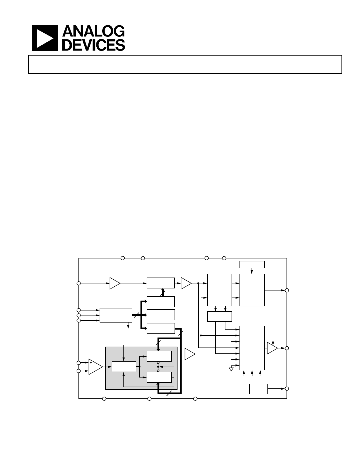
The ADF411x family of frequency synthesizers can be used to
implement local oscillators (LO) in the upconversion and
downconversion sections of wireless receivers and transmitters.
They consist of a low noise digital phase frequency detector
(PFD), a precision charge pump, a programmable reference
divider, programmable A and B counters, and a dual-modulus
prescaler (P/P + 1). The A (5-bit) and B (13-bit) counters, in
conjunction with the dual-modulus prescaler (P/P + 1),
implement an N divider (N = BP + A). In addition, the 14-bit
reference counter (R counter) allows selectable REF
at the PFD input. A complete phase-locked loop (PLL) can be
implemented if the synthesizer is used with an external loop
filter and voltage controlled oscillator (VCO).
All of the on-chip registers are controlled via a simple 3-wire
interface. The devices operate with a power supply ranging
from 2.7 V to 5.5 V and can be powered down when not in use.
FUNCTIONAL BLOCK DIAGRAM
DV
DD
DD
CPGND
P
frequencies
IN
ADF4116/ADF4117/ADF4118
REF
IN
CLK
DATA
LE
A
RF
IN
RF
B
IN
Rev. D
Information furnished by Analog Devices is believed to be accurate and reliable. However, no
responsibility is assumed by Anal og Devices for its use, nor for any infringements of patents or ot her
rights of third parties that may result from its use. Specifications subject to change without notice. No
license is granted by implication or otherwise under any patent or patent rights of Analog Devices.
Trademarks and registered trademarks are the property of their respective owners.
21-BIT
INPUT REGISTER
SD
FROM
FUNCTION LATCH
PRESCALER
P/P + 1
19
OUT
N = BP + A
14-BIT
R COUNTER
R COUNTER
LATCH
FUNCTION
LATCH
A, B COUNTER
LATCH
13
13-BIT
B COUNTER
LOAD
LOAD
5-BIT
A COUNTER
14
5
REFERENCE
PHASE
FREQUENCY
DETECTOR
LOCK
DETECT
18
AV
DD
SD
OUT
DGNDAGNDCE
CHARGE
PUMP
MUX
M3 M2 M1
FL
SWITCH
CP
HIGH Z
MUXOUT
O
FL
O
Figure 1.
One Technology Way, P.O. Box 9106, Norwood, MA 02062-9106, U.S.A.
Tel: 781.329.4700 www.analog.com
Fax: 781.461.3113 ©2000–2007 Analog Devices, Inc. All rights reserved.
00392-001

ADF4116/ADF4117/ADF4118
TABLE OF CONTENTS
Features.............................................................................................. 1
Applications....................................................................................... 1
General Description ......................................................................... 1
Functional Block Diagram .............................................................. 1
Revision History ............................................................................... 2
Specifications..................................................................................... 3
Timing Characteristics ................................................................ 5
Absolute Maximum Ratings............................................................ 6
ESD Caution.................................................................................. 6
Pin Configuration and Function Descriptions............................. 7
Typical Performance Characteristics ............................................. 8
Circuit Description......................................................................... 12
Reference Input Section............................................................. 12
RF Input Stage............................................................................. 12
Prescaler (P/P + 1)...................................................................... 12
A Counter and B Counter......................................................... 12
R Counter ....................................................................................12
Phase Frequency Detector (PFD) and Charge Pump............ 13
MUXOUT and Lock Detect...................................................... 13
Input Shift Register..................................................................... 13
REVISION HISTORY
4/07—Rev. C to Rev. D
Changes to REF
Changes to Table 4............................................................................ 7
Changes to Figure 35...................................................................... 22
Changes to Ordering Guide.......................................................... 25
11/05—Rev. B to Rev. C
Changes to Table 1............................................................................ 3
Changes to Table 2............................................................................ 5
Changes to Table 3............................................................................ 6
Changes to Table 4............................................................................ 7
Changed OSC 3B1-13M0 to FOX801BH-130............................ 21
Changes to Ordering Guide.......................................................... 25
Characteristics Section..................................... 3
IN
Latch Summaries........................................................................ 14
Latch Maps.................................................................................. 15
Function Latch................................................................................ 19
Counter Reset ............................................................................. 19
Power-Down ............................................................................... 19
MUXOUT Control..................................................................... 19
Phase Detector Polarity ............................................................. 19
Charge Pump Three-State......................................................... 19
Fastlock Enable Bit..................................................................... 19
Fastlock Mode Bit....................................................................... 19
Timer Counter Control............................................................. 19
Initialization Latch..................................................................... 20
Device Programming After Initial Power-Up........................ 20
Applications Information.............................................................. 21
Local Oscillator for the GSM Base Station Transmitter........ 21
Shutdown Circuit ....................................................................... 21
Direct Conversion Modulator .................................................. 21
Interfacing ................................................................................... 24
Outline Dimensions....................................................................... 25
Ordering Guide .......................................................................... 25
9/04—Rev. A to Rev. B
Changes to Specifications.................................................................3
Changes to Ordering Guide.......................................................... 25
3/01—Rev. 0 to Rev. A
4/00—Rev. 0: Initial Version
Rev. D | Page 2 of 28

ADF4116/ADF4117/ADF4118
SPECIFICATIONS
AVDD = DVDD = 3 V ± 10%, 5 V ± 10%; AVDD ≤ VP ≤ 6.0 V; AGND = DGND = CPGND = 0 V; TA = T
noted; dBm referred to 50 Ω.
MIN
to T
, unless otherwise
MAX
Table 1.
Parameter B Version
1
Y Version2Unit Test Conditions/Comments
RF CHARACTERISTICS
RF Input Sensitivity −15 to 0 −10 to 0 dBm min to max AV
−10 to 0 −10 to 0 dBm min to max AV
RF Input Frequency
= 3 V
DD
= 5 V
DD
Figure 26 for input circuit
See
ADF4116 80 to 550 MHz min to max
45 to 550 MHz min to max
Input level = −8 dBm; for lower frequencies,
ensure slew rate (SR) > 36 V/μs
ADF4117 0.1 to 1.2 GHz min to max
ADF4118 0.1 to 3.0 0.1 to 3.0 GHz min to max Input level = −10 dBm
0.2 to 3.0 GHz min to max Input level = −15 dBm
, DV
, DV
DD
DD
= 3 V
= 5 V
Maximum Allowable Prescaler
Output Frequency
3
165
200
165
200
MHz max
MHz max
AV
AV
DD
DD
REFIN CHARACTERISTICS
Reference Input Frequency 5 to 100 5 to 100 MHz min to max For f < 5 MHz, ensure SR > 100 V/μs
Reference Input Sensitivity
4, 5
0.4 to AVDD 0.4 to AVDD V p-p min to max AVDD = 3.3 V, biased at AVDD/2
0.7 to AVDD 0.7 to AVDD V p-p min to max For f ≥ 10 MHz, AVDD = 5 V, biased at AVDD/2
REFIN Input Capacitance 10 10 pF max
REFIN Input Current ±100 ±100 μA max
PHASE DETECTOR FREQUENCY5 55 55 MHz max
CHARGE PUMP
I
Sink/Source
CP
High Value 1 1 mA typ
Low Value 250 250 μA typ
Absolute Accuracy 2.5 2.5 % typ
ICP Three-State Leakage Current 3 25 nA max
1 16 nA typ
Sink and Source Current Matching 3 3 % typ 0.5 V ≤ VCP ≤ VP − 0.5
ICP vs. VCP 2 2 % typ 0.5 V ≤ VCP ≤ VP − 0.5
ICP vs. Temperature 2 2 % typ VCP = VP/2
LOGIC INPUTS
V
, Input High Voltage 0.8 × DVDD 0.8 × DVDD V min
INH
V
, Input Low Voltage 0.2 × DVDD 0.2 × DVDD V max
INL
I
, Input Current ±1 ± 1 μA max
INH/IINL
CIN, Input Capacitance 10 10 pF max
Reference Input Current ±100 ± 100 μA max
LOGIC OUTPUTS
VOH, Output High Voltage DVDD − 0.4 DVDD − 0.4 V min IOH = 500 μA
VOL, Output Low Voltage 0.4 0.4 V max IOL = 500 μA
Rev. D | Page 3 of 28

ADF4116/ADF4117/ADF4118
Parameter B Version
1
Y Version2Unit Test Conditions/Comments
POWER SUPPLIES
AVDD 2.7 to 5.5 2.7 to 5.5 V min to V max
DVDD AVDD AVDD
VP AVDD to 6.0 AVDD to 6.0 V min to V max AVDD ≤ VP ≤ 6.0 V
IDD (AIDD + DIDD)
6
ADF4116 5.5 mA max 4.5 mA typical
ADF4117 5.5 mA max 4.5 mA typical
ADF4118 7.5 7.5 mA max 6.5 mA typical
IP 0.4 0.4 mA max TA = 25°C
Low-Power Sleep Mode 1 1 μA typ
NOISE CHARACTERISTICS
ADF4118 Normalized Phase Noise
7
Floor
−213 −213 dBc/Hz typ
Phase Noise Performance8 @ VCO output
ADF4116 540 MHz Output
ADF4117 900 MHz Output
ADF4118 900 MHz Output
9
10
10
−89 −89 dBc/Hz typ @ 1 kHz offset and 200 kHz PFD frequency
−87 −87 dBc/Hz typ @ 1 kHz offset and 200 kHz PFD frequency
−90 −90 dBc/Hz typ @ 1 kHz offset and 200 kHz PFD frequency
ADF4117 836 MHz Output11 −78 −78 dBc/Hz typ @ 300 Hz offset and 30 kHz PFD frequency
ADF4118 1750 MHz Output12 −85 −85 dBc/Hz typ @ 1 kHz offset and 200 kHz PFD frequency
ADF4118 1750 MHz Output13 −65 −65 dBc/Hz typ @ 200 Hz offset and 10 kHz PFD frequency
ADF4118 1960 MHz Output14 −84 −84 dBc/Hz typ @ 1 kHz offset and 200 kHz PFD frequency
Spurious Signals
ADF4116 540 MHz Output
ADF4117 900 MHz Output
ADF4118 900 MHz Output
10
10
10
−88/−99 −88/−99 dBc typ @ 200 kHz/400 kHz and 200 kHz PFD frequency
−90/−104 −90/−104 dBc typ @ 200 kHz/400 kHz and 200 kHz PFD frequency
−91/−100 −91/−100 dBc typ @ 200 kHz/400 kHz and 200 kHz PFD frequency
ADF4117 836 MHz Output11 −80/−84 −80/−84 dBc typ @ 30 kHz/60 kHz and 30 kHz PFD frequency
ADF4118 1750 MHz Output
ADF4118 1750 MHz Output
12
13
−88/−90 −88/−90 dBc typ @ 200 kHz/400 kHz and 200 kHz PFD frequency
−65/−73 −65/−73 dBc typ @ 10 kHz/20 kHz and 10 kHz PFD frequency
ADF4118 1960 MHz Output14 −80/−86 −80/−86 dBc typ @ 200 kHz/400 kHz and 200 kHz PFD frequency
1
Operating temperature range for the B version is −40°C to +85°C.
2
Operating temperature range for the Y version is −40°C to +125°C.
3
This is the maximum operating frequency of the CMOS counters.
4
AC coupling ensures AVDD/2 bias. See Figure 35 for typical circuit.
5
Guaranteed by design.
6
TA = 25°C; AVDD = DVDD = 3 V; RFIN for ADF4116 = 540 MHz; RFIN for ADF4117, ADF4118 = 900 MHz.
7
The synthesizer phase noise floor is estimated by measuring the in-band phase noise at the output of the VCO, PN
: PN
= PN
divider value) and 10logF
8
The phase noise is measured with the EVAL-ADF411xEB and the HP8562E Spectrum Analyzer. The spectrum analyzer provides the REFIN for the synthesizer
= 10 MHz @ 0 dBm).
(f
REFOUT
9
f
= 10 MHz; f
REFIN
10
f
= 10 MHz; f
REFIN
11
f
= 10 MHz; f
REFIN
12
f
= 10 MHz; f
REFIN
13
f
= 10 MHz; f
REFIN
14
f
= 10 MHz; f
REFIN
PFD
SYNTH
= 200 kHz; offset frequency = 1 kHz; fRF = 540 MHz; N = 2700; loop bandwidth = 20 kHz.
PFD
= 200 kHz; offset frequency = 1 kHz; fRF = 900 MHz; N = 4500; loop bandwidth = 20 kHz.
PFD
= 30 kHz; offset frequency = 300 Hz; fRF = 836 MHz; N = 27867; loop bandwidth = 3 kHz.
PFD
= 200 kHz; offset frequency = 1 kHz; fRF = 1750 MHz; N = 8750; loop bandwidth = 20 kHz.
PFD
= 10 kHz; offset frequency = 200 Hz; fRF = 1750 MHz; N = 175000; loop bandwidth = 1 kHz.
PFD
= 200 kHz; offset frequency = 1 kHz; fRF = 1960 MHz; N = 9800; loop bandwidth = 20 kHz.
PFD
– 10logF
TOT
– 20logN.
PFD
, and subtracting 20logN (where N is the N
TOT
Rev. D | Page 4 of 28
ADF4116/ADF4117/ADF4118
A
TIMING CHARACTERISTICS
AVDD = DVDD = 3 V ± 10%, 5 V ± 10%; AVDD ≤ VP < 6.0 V; AGND = DGND = CPGND = 0 V; TA = T
Guaranteed by design, but not production tested.
Table 2.
Parameter Limit at T
MIN
to T
(B, Y Version) Unit Test Conditions/Comments
MAX
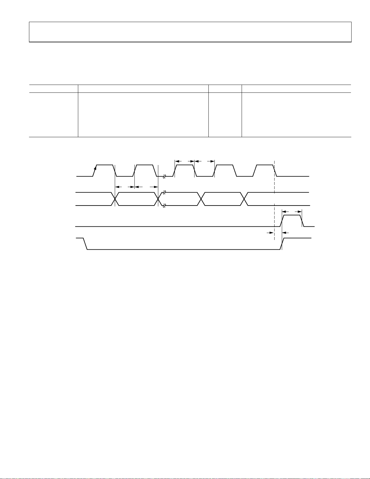
t1 10 ns min DATA to CLK setup time
t2 10 ns min DATA to CLK hold time
t3 25 ns min CLK high duration
t4 25 ns min CLK low duration
t5 10 ns min CLK to LE setup time
t6 20 ns min LE pulse width
t
4
CLK
t
3
MIN
to T
, unless otherwise noted.
MAX
t
2
DB1
(CONTROL BIT C2)
DB0 (LSB)
(CONTROL BIT C1)
t
5
t
6
00392-002
DAT
t
1
DB20 (MSB) DB19 DB2
LE
LE
Figure 2. Timing Diagram
Rev. D | Page 5 of 28
ADF4116/ADF4117/ADF4118
ABSOLUTE MAXIMUM RATINGS
TA = 25°C, unless otherwise noted.
Table 3.
Parameter Rating
AVDD to GND1 −0.3 V to +7 V
AVDD to DVDD −0.3 V to +0.3 V
VP to GND1 −0.3 V to +7 V
VP to AVDD −0.3 V to +5.5 V
Digital I/O Voltage to GND1 −0.3 V to VDD + 0.3 V
Analog I/O Voltage to GND1 −0.3 V to VP + 0.3 V
REFIN, RFINA, RFINB to GND1 −0.3 V to VDD + 0.3 V
RFINA to RFINB ±320 mV
Operating Temperature Range
Industrial (B Version) −40°C to +85°C
Extended (Y Version) −40°C to +125°C
Storage Temperature Range −65°C to +150°C
Maximum Junction Temperature 150°C
TSSOP θJA Thermal Impedance 112°C/W
Reflow Soldering
Peak Temperature 260°C
Time at Peak Temperature 40 sec
Transistor Count
CMOS 6425
Bipolar 303
1
GND = AGND = DGND = 0 V.
Stresses above those listed under Absolute Maximum Ratings
may cause permanent damage to the device. This is a stress
rating only; functional operation of the device at these or any
other conditions above those indicated in the operational
section of this specification is not implied. Exposure to absolute
maximum rating conditions for extended periods may affect
device reliability.
This device is a high performance RF integrated circuit with an
ESD rating of <2 kV, and it is ESD sensitive. Proper precautions
should be taken for handling and assembly.
ESD CAUTION
Rev. D | Page 6 of 28
ADF4116/ADF4117/ADF4118
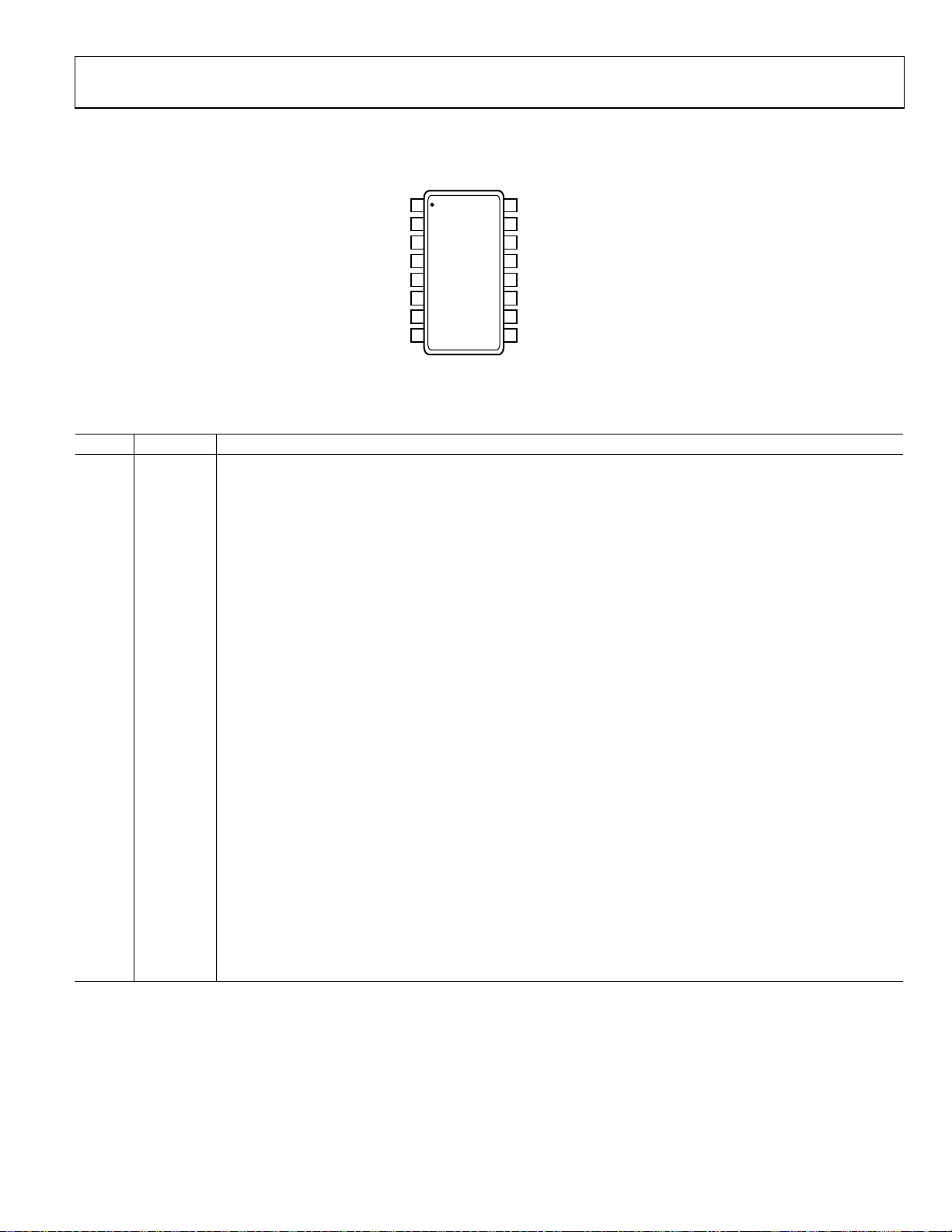
PIN CONFIGURATION AND FUNCTION DESCRIPTIONS
FL
CP
CPGND
AGND
RF
IN
RFINA
AV
REF
O
B
DD
IN
1
2
ADF4116/
3
ADF4117/
4
ADF4118
5
TOP VIEW
(Not to Scale)
6
7
8
16
15
14
13
12
11
10
9
V
P
DV
DD
MUXOUT
LE
DATA
CLK
CE
DGND
00392-003
Figure 3. Pin Configuration
Table 4. Pin Function Descriptions
Pin No. Mnemonic Description
1 FLO
Fast Lock Switch Output. This can be used to switch an external resistor to change the loop filter bandwidth
and speed up locking the PLL.
2 CP
Charge Pump Output. When enabled, this provides the ± I
to the external loop filter, which in turn drives the
CP
external VCO.
3 CPGND Charge Pump Ground. This is the ground return path for the charge pump.
4 AGND Analog Ground. This is the ground return path for the prescaler.
5 RFINB
Complementary Input to the RF Prescaler. This point should be decoupled to the ground plane with a small
bypass capacitor, typically 100 pF. See
Figure 26.
6 RFINA Input to the RF Prescaler. This small signal input is ac-coupled from the VCO.
7 AVDD
8 REFIN
Analog Power Supply. This can range from 2.7 V to 5.5 V. Decoupling capacitors to the analog ground plane
should be placed as close as possible to this pin. AV
Reference Input. This is a CMOS input with a nominal threshold of V
See
Figure 25. The oscillator input can be driven from a TTL or CMOS crystal oscillator, or it can be ac-coupled.
must have the same value as DVDD.
DD
/2 and an equivalent input resistance of 100 kΩ.
DD
9 DGND Digital Ground.
10 CE
Chip Enable. A logic low on this pin powers down the device and puts the charge pump output into three-state
mode. Taking the pin high powers up the device depending on the status of the power-down bit F2.
11 CLK
Serial Clock Input. This serial clock is used to clock in the serial data to the registers. The data is latched into the
21-bit shift register on the CLK rising edge. This input is a high impedance CMOS input.
12 DATA
Serial Data Input. The serial data is loaded MSB first with the two LSBs as the control bits. This input is a high
impedance CMOS input.
13 LE
Load Enable, CMOS Input. When LE goes high, the data stored in the shift registers is loaded into one of the four
latches, the latch being selected using the control bits.
14 MUXOUT
This multiplexer output allows either the lock detect, the scaled RF, or the scaled reference frequency to be
accessed externally.
15 DVDD
Digital Power Supply. This can range from 2.7 V to 5.5 V. Decoupling capacitors to the digital ground plane (1 μF, 1 nF)
should be placed as close as possible to this pin. For best performance, the 1 μF capacitor should be placed within 2 mm
of the pin. The placing of the 1 nF capacitor is less critical, but should still be within 5 mm of the pin.
must have the same value as AVDD.
DV
DD
16 VP
Charge Pump Power Supply. This should be greater than or equal to V
. In systems where VDD is 3 V, this supply can
DD
be set to 6 V and used to drive a VCO with a tuning range of up to 6 V.
Rev. D | Page 7 of 28
ADF4116/ADF4117/ADF4118
TYPICAL PERFORMANCE CHARACTERISTICS
PARAM-TYPE DATA-F ORMAT KEYWORD IMPEDANCE-
FREQUNIT
GHz S MA R 50
FREQ MagS11 AngS11
0.05 0.89207 –2.0571
0.10 0.8886 –4.4427
0.15 0.89022 –6.3212
0.20 0.96323 –2.1393
0.25 0.90566 –12.13
0.30 0.90307 –13.52
0.35 0.89318 –15.746
0.40 0.89806 –18.056
0.45 0.89565 –19.693
0.50 0.88538 –22.246
0.55 0.89699 –24.336
0.60 0.89927 –25.948
0.65 0.87797 –28.457
0.70 0.90765 –29.735
0.75 0.88526 –31.879
0.80 0.81267 –32.681
0.85 0.90357 –31.522
0.90 0.92954 –34.222
FREQ MagS11 AngS11
0.95 0.92087 –36.961
1.00 0.93788 –39.343
1.05 0.9512 –40.134
1.10 0.93458 –43.747
1.15 0.94782 –44.393
1.20 0.96875 –46.937
1.25 0.92216 –49.6
1.30 0.93755 –51.884
1.35 0.96178 –51.21
1.40 0.94354 –53.55
1.45 0.95189 –56.786
1.50 0.97647 –58.781
1.55 0.98619 –60.545
1.60 0.95459 –61.43
1.65 0.97945 –61.241
1.70 0.98864 –64.051
1.75 0.97399 –66.19
1.80 0.97216 –63.775
OHMS
–40
–50
–60
–70
–80
–90
–100
–110
PHASE NOISE (dBc/Hz)
–120
–130
–140
00392-004
100Hz FREQUENCY OF FSET F ROM 900MHz CARRIER 1MHz
RL= –40dBc/Hz10dB/DIVI SION RMS NOISE = 0.64°
0.64° rms
00392-007
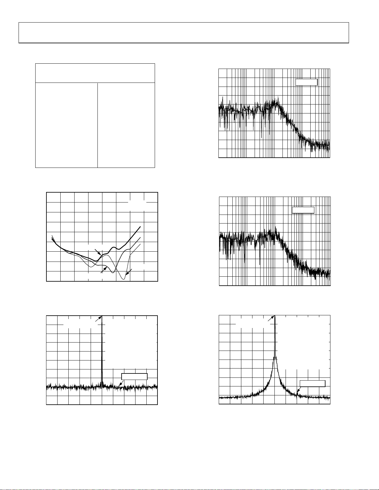
Figure 4. S-Parameter Data for the ADF4118 RF Input (Up to 1.8 GHz)
Figure 7. ADF4118 Integrated Phase Noise
(900 MHz, 200 kHz, 35 kHz, Typical Lock Time: 200 μs)
0
–5
–10
–15
–20
–25
–30
RF INPUT POW ER (dBm)
–35
–40
–45
04
TA = –40°C
= +25°C
T
A
1.0
RF INPUT FREQUENCY (GHz)
VDD = 3V
V
= 3V
P
T
= +85°C
A
00392-005
.00.5 1.5 2.0 2.5 3.0 3.5
Figure 5. Input Sensitivity (ADF4118)
–40
–50
–60
–70
–80
–90
–100
–110
PHASE NOISE (dBc/Hz)
–120
–130
–140
100Hz FREQUENCY OF FSET F ROM 900MHz CARRIER 1MH
Figure 8. ADF4118 Integrated Phase Noise
(900 MHz, 200 kHz, 20 kHz, Typical Lock Time: 400 μs)
0
–10
–20
–30
–40
–50
–60
–70
OUTPUT PO WER (dB)
–80
–90
–100
–400kHz –200kHz 900MHz 200kHz 400kHz
–10
–20
–30
–40
–50
–60
–70
OUTPUT PO WER (dB)
–80
–90
–100
0
REFERENCE
LEVEL = –4.2dBm
–2kHz –1kHz 900MHz 1kHz 2kHz
= 3V, VP = 5V
V
DD
I
= 1mA
CP
PFD FREQ UENCY = 200kHz
LOOP BANDWI DTH = 20kHz
RES. BANDWIDT H = 10Hz
VIDEO BANDWIDTH = 10Hz
SWEEP = 1.9 SECO NDS
AVERAGES = 22
–90.2dBc/Hz
00392-006
Figure 6. ADF4118 Phase Noise
(900 MHz, 200 kHz, 20 kHz)
RL= –40dBc/Hz10dB/DIVI SION RMS NOISE = 0.575°
0.575° rms
REFERENCE
LEVEL = –3.8dBm
V
= 3V, VP = 5V
DD
= 1mA
I
CP
PFD FREQ UENCY = 200kHz
LOOP BANDW IDTH = 20kHz
RES. BANDWIDT H = 1kHz
VIDEO BANDWI DTH = 1kHz
SWEEP = 2.5 SECONDS
AVERAGES = 4
Figure 9. ADF4118 Reference Spurs
(900 MHz, 200 kHz, 20 kHz)
–91.5dBc
00392-008
z
00392-009
Rev. D | Page 8 of 28
ADF4116/ADF4117/ADF4118
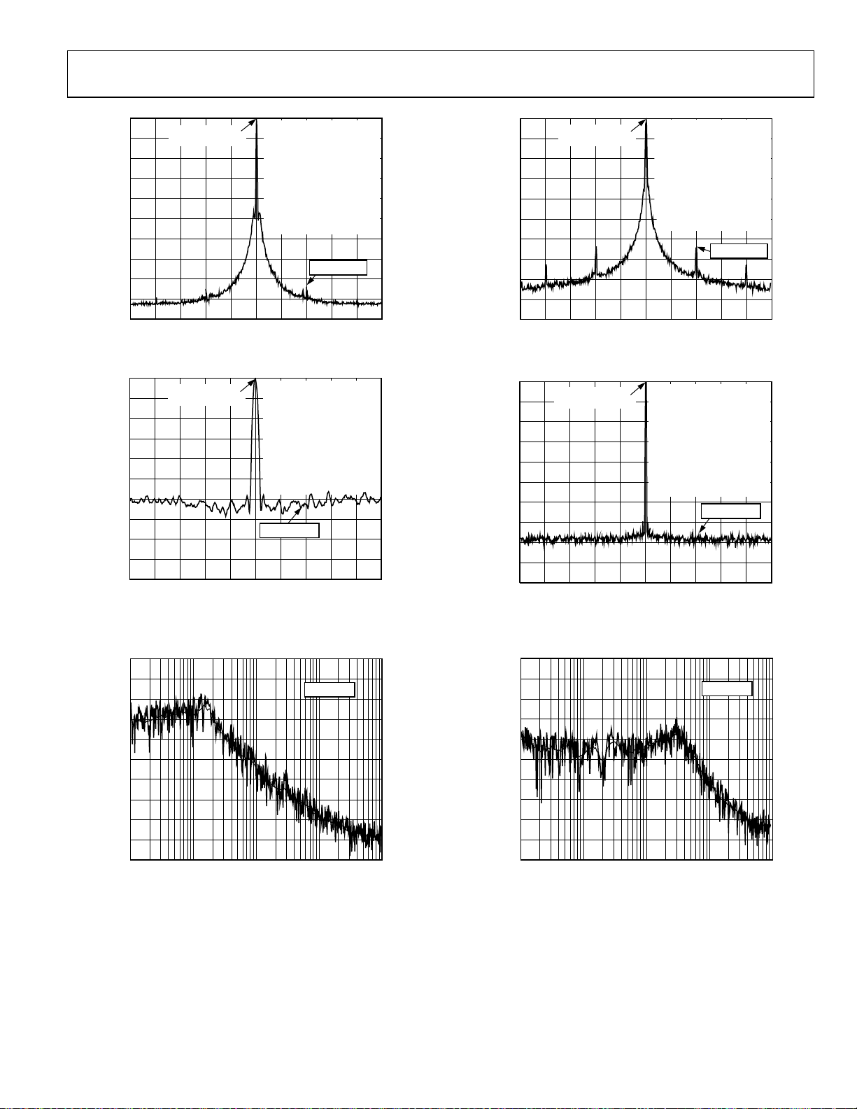
–10
–20
–30
–40
–50
–60
–70
OUTPUT POW ER (dB)
–80
–90
–100
0
REFERENCE
LEVEL = –4.2dBm
–400kHz –200kHz 900MHz 200kHz 400kHz
V
= 3V, VP = 5V
DD
= 1mA
I
CP
PFD FREQ UENCY = 200kHz
LOOP BANDW IDTH = 35kHz
RES. BANDWIDTH = 1kHz
VIDEO BANDWI DTH = 1kHz
SWEEP = 2.5 SECONDS
AVERAGES = 10
–90.67dBc
Figure 10. ADF4118 Reference Spurs
(900 MHz, 200 kHz, 35 kHz)
OUTPUT PO WER (dB)
–100
0
–10
–20
–30
–40
–50
–60
–70
–80
–90
REFERENCE
LEVEL = –7.0dBm
–400kHz –200kHz 1750MHz 200kHz 400kHz
V
= 3V, VP = 5V
DD
= 1mA
I
CP
PFD FREQUENCY = 30kHz
LOOP BANDW IDTH = 5kHz
RES. BANDWIDT H = 10kHz
VIDEO BANDWI DTH = 10kHz
SWEEP = 477ms
AVERAGES = 25
–71.5dBc/Hz
Figure 11. ADF4118 Phase Noise
(1750 MHz, 30 kHz, 3 kHz)
–40
–50
–60
–70
–80
–90
–100
–110
PHASE NOISE ( dBc/Hz)
–120
–130
–140
100Hz FREQUENCY OF FSET F ROM 1.75GHz CARRIER 1MHz
RL = –40dBc/Hz10dB/DIVI SION RMS NOI SE = 2.0°
2.0° rms
Figure 12. ADF4118 Integrated Phase Noise
(1750 MHz, 30 kHz, 3 kHz)
00392-010
00392-011
00392-012
OUTPUT PO WER (dB)
–100
0
–10
–20
–30
–40
–50
–60
–70
–80
–90
REFERENCE
LEVEL = –7.0dBm
–60kHz –30k Hz 1750MHz 30kHz 60kHz
V
= 3V, VP = 5V
DD
I
= 5mA
CP
PFD FREQ UENCY = 30kHz
LOOP BANDWI DTH = 5kHz
RES. BANDWIDTH = 300Hz
VIDEO BANDWIDTH = 300Hz
SWEEP = 4.2ms
AVERAGES = 20
–72.3dBc
Figure 13. ADF4118 Reference Spurs
(1750 MHz, 30 kHz, 3 kHz)
–10
–20
–30
–40
–50
–60
–70
OUTPUT PO WER (dB)
–80
–90
–100
0
REFERENCE
LEVEL = –10.3dBm
–2kHz –1kHz
VVDD = 3V, VP = 5V
= 1mA
I
CP
PFD FREQUENCY = 1MHz
LOOP BANDW IDTH = 100kHz
RES. BANDWIDT H = 10Hz
VIDEO BANDWI DTH = 10Hz
SWEEP = 1.9 SECONDS
AVERAGES = 26
–85.2dBc/Hz
2800MHz
1kHz 2kHz
Figure 14. ADF4118 Phase Noise
(2800 MHz, 1 MHz, 100 kHz)
10dB/DIVI SION RL = –40dBc/Hz RMS NOISE = 1. 552°
–40
–50
–60
–70
–80
–90
–100
–110
PHASE NOISE (dBc/Hz)
–120
–130
–140
100Hz FREQUENCY OFFS ET FROM 2.8GHz CARRIE R 1MHz
1.55° rms
Figure 15. ADF4118 Integrated Phase Noise
(2800 MHz, 1 MHz, 100 kHz)
00392-013
00392-014
00392-015
Rev. D | Page 9 of 28

ADF4116/ADF4117/ADF4118
–
–
–
–
–10
–20
–30
–40
–50
–60
–70
OUTPUT PO WER (dB)
–80
–90
–100
0
REFERENCE
LEVEL = –9.3dBm
–2MHz –1M Hz 1MHz 2MHz
VDD = 3V, VP= 5V
= 1mA
I
CP
PFD FREQUENCY = 1MHz
LOOP BANDW IDTH = 100kHz
RES. BANDWIDT H = 3kHz
VIDEO BANDWI DTH = 3kHz
SWEEP = 1. 4 SECONDS
AVERAGES = 4
2800MHz
Figure 16. ADF4118 Reference Spurs
(2800 MHz, 1 MHz, 100 kHz)
130
–135
–140
–145
–150
–155
–160
PHASE NOISE (dBc/Hz)
–165
–170
–175
1 10000100 1000
10
PHASE DETECTO R FREQUENCY (kHz)
Figure 17. ADF4118 Phase Noise (Referred to CP Output) vs.
PFD Frequency
60
–70
–77.3dBc
VDD = 3V
VP = 5V
VDD = 3V
V
= 5V
P
60
VDD = 3V
V
= 5V
P
–70
–80
–90
FIRST REF ERENCE SPUR (dBc)
00392-016
–100
–20 0 20 40 60 80 100
–40
TEMPERATURE ( °C)
00392-019
Figure 19. ADF4118 Reference Spurs vs. Temperature
(900 MHz, 200 kHz, 20 kHz)
5
–5
–15
–25
–35
–45
–55
–65
–75
FIRST REF ERENCE SPUR (dBc)
–85
–95
00392-017
–105
0
1
234
TUNING VOLTAGE
Figure 20. ADF4118 Reference Spurs (200 kHz) vs. V
VDD = 3V
V
= 5V
P
TUNE
00392-020
5
(900 MHz, 200 kHz, 20 kHz)
60
–70
VDD = 3V
V
= 5V
P
–80
–80
PHASE NOISE ( dBc/Hz)
–90
–100
–20 0 20 40 60 80 100
–40
TEMPERATURE ( °C)
Figure 18. ADF4118 Phase Noise vs. Temperature
(900 MHz, 200 kHz, 20 kHz)
00392-018
PHASE NOISE (dBc/Hz)
–90
020406080
TEMPERATURE ( °C)
Figure 21. ADF4118 Phase Noise vs. Temperature
(836 MHz, 30 kHz, 3 kHz)
00392-021
100
Rev. D | Page 10 of 28

ADF4116/ADF4117/ADF4118
–
60
–70
–80
–90
FIRST REF ERENCE SPUR (dBc)
–100
0
20 40 60 80 100
TEMPERATURE (°C)
Figure 22. ADF4118 Reference Spurs vs. Temperature
(836 MHz, 30 kHz, 3 kHz)
3.0
2.5
2.0
(mA)
1.5
DD
DI
1.0
VDD = 3V
V
= 5V
P
00392-022
1.2
1.0
0.8
0.6
0.4
0.2
0
(mA)
CP
I
–0.2
–0.4
–0.6
–0.8
–1.0
–1.2
0.5 1.5 2.0 2.5 3.0 3.5 4.5 5.0
01.0
VCP (V)
VP = 5V
I
SETTING: 1mA
CP
4.0
00392-024
Figure 24. Charge Pump Output Characteristics
0.5
0
0
50 100 150 200
PRESCALER OUTPUT FREQUENCY (MHz)
00392-023
Figure 23. DIDD vs. Prescaler Output Frequency
Rev. D | Page 11 of 28

ADF4116/ADF4117/ADF4118
(
[
×+×
=
CIRCUIT DESCRIPTION
REFERENCE INPUT SECTION
The reference input stage is shown in Figure 25. SW1 and SW2
are normally closed switches; SW3 is normally open. When
power-down is initiated, SW3 is closed and SW1 and SW2 are
opened. This ensures that there is no loading of the REF
IN
pin
on power-down.
POWE R-DOWN
CONTROL
100kΩ
NC
REF
IN
NC
SW1
Figure 25. Reference Input Stage
SW2
SW3
NO
BUFFER
TO R COUNTER
00392-025
RF INPUT STAGE
The RF input stage is shown in Figure 26. It is followed by a
2-stage limiting amplifier to generate the CML clock levels
needed for the prescaler.
1.6V
AV
DD
500Ω500Ω
AGND
00392-026
RFINA
RF
IN
BIAS
GENERATOR
B
Figure 26. RF Input Stage
PRESCALER (P/P + 1)
The dual-modulus prescaler (P/P + 1), along with the A counter
and B counter, enables the large division ratio, N, to be realized
(N = PB + A). The dual-modulus prescaler takes the CML clock
from the RF input stage and divides it down to a manageable
frequency for the CMOS A counter and CMOS B counter. The
prescaler is programmable. It can be set in software to 8/9 for the
ADF4116 and to 32/33 for the ADF4117 and ADF4118. It is based
on a synchronous 4/5 core.
A COUNTER AND B COUNTER
The A CMOS counter and B CMOS counter combine with the
dual-modulus prescaler to allow a wide ranging division ratio in
the PLL feedback counter. The counters are specified to work
when the prescaler output is 200 MHz or less.
Pulse Swallow Function
The A counter and B counter, in conjunction with the dualmodulus prescaler, make it possible to generate output
frequencies that are spaced only by the reference frequency
divided by R. The equation for the VCO frequency is as follows:
VCO
)
REFIN
RfABPf
/
]
where:
is the output frequency of external voltage controlled
f
VCO
oscillator (VCO).
P is the preset modulus of dual-modulus prescaler.
B is the preset divide ratio of binary 13-bit counter (3 to 8191).
A is the preset divide ratio of binary 5-bit swallow counter (0 to 31).
f
is the output frequency of the external reference frequency
REFIN
oscillator.
R is the preset divide ratio of binary 14-bit programmable
reference counter (1 to 16,383).
R COUNTER
The 14-bit R counter allows the input reference frequency to be
divided down to produce the input clock to the phase frequency
detector (PFD). Division ratios from 1 to 16,383 are allowed.
FROM RF
INPUT STAGE
MODULUS
CONTROL
N = BP + A
13-BIT
B COUNTER
PRESCALER
P/P + 1
Figure 27. A Counter and B Counter
LOAD
LOAD
5-BIT
A COUNTER
TO PFD
00392-027
Rev. D | Page 12 of 28

ADF4116/ADF4117/ADF4118
V
A
PHASE FREQUENCY DETECTOR (PFD) AND CHARGE PUMP
The PFD takes inputs from the R counter and N counter and
produces an output proportional to the phase and frequency
difference between them.
the PFD. The PFD includes a fixed delay element that sets the
width of the antibacklash pulse. This is typically 3 ns. This pulse
ensures that there is no dead zone in the PFD transfer function
and gives a consistent reference spur level.
HI
R DIVIDER
HI
N DIVIDER
R DIVIDER
N DIVIDER
CP OUTPUT
Figure 28. PFD Simplified Schematic and Timing (In Lock)
CLR1
CLR2
Figure 28 is a simplified schematic of
UP
Q1D1
U1
DELAY
DOWN
Q2D2
U2
U3
CPGND
P
CHARGE
PUMP
CP
00392-028
MUXOUT AND LOCK DETECT
The output multiplexer on the ADF411x family allows the user
to access various internal points on the chip. The state of
MUXOUT is controlled by M3, M2, and M1 in the function
latch.
Figure 33 shows the full truth table. Figure 29 shows the
MUXOUT section in block diagram form.
DV
DD
NALOG LO CK DETECT
DIGITAL LOCK DET ECT
R COUNTER OUT PUT
N COUNTER OUT PUT
SDOUT
CONTROLMUX
MUXOUT
DGND
Figure 29. MUXOUT Circuit
Lock Detect
MUXOUT can be programmed for both digital lock detect and
analog lock detect.
Digital lock detect is active high. It is set high when the phase
error on three consecutive phase detector cycles is less than
15 ns. It stays set high until a phase error greater than 25 ns is
detected on any subsequent PD cycle.
The N channel, open-drain, analog lock detect should be
operated with an external pull-up resistor of 10 kΩ nominal.
When lock is detected, it is high with narrow low going pulses.
INPUT SHIFT REGISTER
The ADF411x family digital section includes a 21-bit input shift
register, a 14-bit R counter, and an 18-bit N counter, comprising
a 5-bit A counter and a 13-bit B counter. Data is clocked into
the 21-bit shift register on each rising edge of CLK. The data is
clocked in MSB first. Data is transferred from the shift register
to one of four latches on the rising edge of LE. The destination
latch is determined by the state of the two control bits (C2, C1)
in the shift register. These are the two LSBs, DB1 and DB0, as
shown in the timing diagram in
these bits is shown in
Figure 34. Ta b le 5 summarizes how the
latches are programmed.
Figure 2. The truth table for
00392-029
Table 5. Programming Data Latches
Control Bits
C2 C1 Data Latch
0 0 R Counter
0 1 N Counter (A and B)
1 0 Function Latch
1 1 Initialization Latch
Rev. D | Page 13 of 28

ADF4116/ADF4117/ADF4118
LATCH SUMMARIES
REFERENCE COUNTER LATCH
TEST
LOCK
DETECT
PRECISION
DB20 DB19 DB18 DB17 DB16 DB15 DB14 DB13 DB12 DB11 DB9 DB8 DB7 DB6 DB5 DB4 DB3 DB2 DB1 DB0DB10
LDP T4 T3 T2 T1 R14 R13 R12 R11 R10 R8 R7 R6 R5 R4 R3 R2 R1 C2 ( 0) C1 (0)R9
MODE BITS
14-BIT REFE RENCE COUNTER, R
AB COUNTER LATCH
CP GAIN
DB20 DB19 DB18 DB17 DB16 DB15 DB14 DB13 DB12 DB 11 DB9 DB8 DB7 DB6 DB5 DB4 DB3 DB2 DB1 DB0DB10
G1 B13 B12 B11 B10 B9 B8 B7 B6 B5 B3 B2 B1 A5 A4 A3 A2 A1 C2 ( 0) C1 (1)B4
13-BIT B COUNT ER 5-BIT A COUNTER
FUNCTION LATCH
RESERVED
DOWN 2
POWER-
RESERVED
DB19 DB18 DB17 DB16 DB15 DB14 DB13 DB12 DB 11 DB9 DB8 DB7 DB6 DB5 DB4 DB3 DB2 DB1 DB0DB10
DB20
PD2X
XXX
TIMER COUNTER
CONTROL
TC4 TC3 TC2 TC1 F6 F4 F3 F2 M3 M2 M1 PD1 F1 C2 (1) C1 (0)
MODE
FAS TLO CK
X
CONTROL
BITS
CONTRO L
BITS
CP
STATE
PHASE
THREE-
ENABLE
RESERVED
FAS TLO CK
DETECTOR
MUXOUT
CONTROL
POLARITY
DOWN 1
POWER-
CONTRO L
BITS
RESET
COUNTER
INITIALIZATION LATCH
RESERVED
DOWN 2
POWER-
RESERVED
DB20 DB19 DB18 DB17 DB16 DB15 DB14 DB13 DB12 DB 11 DB9 DB8 DB7 DB6 DB5 DB4 DB3 DB2 DB1 DB0DB10
X
XXX
PD2 TC4 TC3 TC2 TC1 F6 F4 F 3 F2 M 3 M2 M1 PD1 F 1 C2 (1) C1 (1)
TIMER COUNTER
CONTROL
MODE
FAS TLO CK
RESERVED
X
CP
STATE
PHASE
THREE-
ENABLE
FAS TLO CK
DETECTOR
Figure 30. ADF411x family Latch Summary
Rev. D | Page 14 of 28
MUXOUT
CONTROL
POLARITY
DOWN 1
POWER-
CONTROL
BITS
RESET
COUNTER
00392-030

ADF4116/ADF4117/ADF4118
LATCH MAPS
TEST
LOCK
DETECT
PRECISION
DB20 DB19 DB18 DB17 DB16 DB15 DB14 DB13 DB12 DB11 DB9 DB8 DB7 DB6 DB5 DB4 DB3 DB2 DB1 DB0DB10
LDP T4 T3 T 2 T1 R14 R13 R12 R11 R10 R8 R7 R6 R5 R4 R3 R2 R1 C2 (0) C1 (0)R9
MODE BITS
TEST MODE BITS SHOULD
BE SET TO 0000 FOR
NORMAL OPERAT ION
14-BIT REFERE NCE COUNTER, R
R14
0
0
0
0
•
•
•
1
1
1
1
R13
0
0
0
0
•
•
•
1
1
1
1
R12
CONTROL
BITS
••••••••••
0
••••••••••
0
••••••••••
0
••••••••••
0
••••••••••
•
••••••••••
•
••••••••••
•
••••••••••
1
••••••••••
1
••••••••••
••••••••••
1
1
••••••••••
R3 R2 R1 DIVIDE RATIO
0
0
1
0
1
0
0
1
•
•
•
•
•
•
0
1
0
1
1
1
1
1
1
0
1
0
•
•
•
0
1
0
1
1
2
3
4
•
•
•
163 80
163 81
163 82
163 83
OPERATIONLDP
3 CONSECUTIVE CYCLES OF PHASE DELAY LESS THAN
0
15ns MUST OCCUR BEFORE LO CK DETECT IS SET.
5 CONSECUTIVE CYCLES OF PHASE DELAY LESS THAN
1
15ns MUST OCCUR BEFORE LO CK DETECT IS SET.
Figure 31. Reference Counter Latch Map
00392-031
Rev. D | Page 15 of 28

ADF4116/ADF4117/ADF4118
CP GAIN
13-BIT B COUNTE R 5-BIT A COUNTER
DB20 DB19 DB18 DB17 DB16 DB15 DB14 DB13 DB12 DB11 DB9 DB8 DB7 DB6 DB5 DB4 DB3 DB2 DB1 DB0DB10
G1 B13 B12 B11 B10 B9 B8 B7 B6 B5 B3 B2 B1 A5 A4 A3 A2 A1 C2 (0) C1 (1)B4
ADF4116
ADF4117/ADF4118
CONTROL
BITS
A5
X
X
•
•
X
X
A5
0
0
0
•
•
1
1
1
A4
X
X
•
•
X
X
A4
0
0
0
•
•
1
1
1
A3
0
0
•
•
1
1
A3
0
0
0
•
•
1
1
1
A2
0
0
•
•
1
1
A2
0
0
1
•
•
0
1
1
A1
0
1
•
•
0
1
A1
0
1
0
•
•
1
0
1
A COUNTER
DIVIDE RATIO
0
1
•
•
6
7
A COUNTER
DIVIDE RATIO
0
1
2
•
•
29
30
31
••••••••••
B13
0
0
0
0
•
•
•
1
1
1
1
CURRENT SETTI NGSLDP
250µA
0
1
1mA
B12
0
0
0
0
•
•
•
1
1
1
1
B11
0
••••••••••
0
••••••••••
0
••••••••••
0
••••••••••
•
••••••••••
•
••••••••••
•
••••••••••
1
••••••••••
1
••••••••••
1
••••••••••
1
••••••••••
B3 B2 B1 B COUNTER DIVIDE RATI O
0
0
0
1
•
•
•
1
1
1
1
0
1
1
0
•
•
•
0
0
1
1
1
0
1
0
•
•
•
0
1
0
1
NOT ALLO WED
NOT ALLO WED
3
4
•
•
•
8188
8189
8190
8191
N = BP + A, P IS P RESCALER VALUE. B MUST BE GREATER
THAN OR EQUAL T O A. FO R CONTINUOUS LY ADJACENT
VALUES OF N
X FREF
, N
MIN
IS (P2 – P).
00392-032
Figure 32. A Counter/B Counter Latch Map
Rev. D | Page 16 of 28

ADF4116/ADF4117/ADF4118
RESERVED
DOWN 2
POWER-
RESERVED
DB19 DB18 DB17 DB16 DB15 DB14 DB13 DB12 DB11 DB9 DB8 DB7 DB6 DB5 DB4 DB3 DB2 DB1 DB0DB10
DB20
PD2X
XXX
CE PIN PD2 PD1 MODE
ASYNCHRONOUS POWER-DOWN
X
X
0
NORMAL OPERAT ION
0
X
1
ASYNCHRONOUS POWER-DOWN
1
0
1
SYNCHRONOUS POW ER-DOWN
1
1
1
TC4
TIMER COUNTER
CONTROL
TC4 TC3 TC2 TC1 F6 F4 F3 F2 M3 M2 M1 PD1 F1 C2 (1) C1 (0)
F4
0
1
1
TC3
0
0
0
0
0
0
0
0
1
1
1
1
1
1
1
1
0
0
0
0
1
1
1
1
0
0
0
0
1
1
1
1
TC2
0
0
1
1
0
0
1
1
0
0
1
1
0
0
1
1
TC1
0
1
0
1
0
1
0
1
0
1
0
1
0
1
0
1
MODE
RESERVED
FASTLOCK
X
F6
FASTLOCK MODE
X
FASTLOCK DISABLED
0
FASTLOCK MODE 1
1
FASTLOCK MODE 2
TIMEOUT
(PFD CYCLES)
3
7
11
15
19
23
27
31
35
39
43
47
51
55
59
63
CP
STATE
THREE-
F3
0
1
PHASE
DETECT OR
F2
0
1
CHARGE PUMP
OUTPUT
NORMAL
THREE-STAT E
ENABLE
FASTLOCK
MUXOUT
CONTROL
POLARITY
M2
M3
0
0
0
0
1
0
1
0
0
1
0
1
1
1
1
1
PHASE DETECTOR
POLARITY
NEGATIVE
POSITIVE
DOWN 1
POWER-
COUNTER
F1
0
NORMAL
R, A, B COUNTERS
1
HELD IN RESET
M1
0
THREE-STATE OUTPUT
DIGITAL LOCK DETECT
1
(ACTIVE HIGH)
N DIVIDER OUTPUT
0
AV
1
0
1
0
1
DD
R DIVIDER OUTPUT
ANALOG LO CK DETECT
(N CHANNEL OPEN DRAIN)
SERIAL DATA O UTPUT
(INVERSE POLARITY OF
SERIAL DATA I NPUT)
DGND
Figure 33. Function Latch Map
CONTROL
BITS
RESET
COUNTER
OPERATIO N
OUTPUT
00392-033
Rev. D | Page 17 of 28

ADF4116/ADF4117/ADF4118
RESERVED
DOWN 2
POWER-
RESERVED
DB20 DB19 DB18 DB17 DB16 DB15 DB14 DB13 DB12 DB11 DB9 DB8 DB7 DB6 DB5 DB4 DB3 DB2 DB1 DB0DB10
X
CE PIN PD2 PD1 MODE
X
0
X
1
0
1
1
1
XXX
PD2 TC4 T C3 TC2 TC1 F6 F4 F3 F2 M3 M2 M1 PD1 F1 C2 (1) C1 (1)
ASYNCHRONOUS POWER-DOWN
X
NORMAL OPERATION
0
ASYNCHRONOUS POWER-DOWN
1
SYNCHRONOUS POWER-DOWN
1
TC4
0
0
0
0
0
0
0
0
1
1
1
1
1
1
1
1
TIMER COUNT ER
CONTRO L
TC3
0
0
0
0
1
1
1
1
0
0
0
0
1
1
1
1
TC2
F4
0
1
1
TC1
0
0
1
1
0
0
1
1
0
0
1
1
0
0
1
1
0
1
0
1
0
1
0
1
0
1
0
1
0
1
0
1
Figure 34. Initialization Latch Map
MODE
FAST LOCK
RESERVED
X
F6
FASTLOCK MODE
FASTLOCK DISABLED
X
FASTLOCK MODE 1
0
FASTLOCK MODE 2
1
TIMEOUT
(PFD CYCLES)
3
7
11
15
19
23
27
31
35
39
43
47
51
55
59
63
CP
STATE
PHASE
THREE-
ENABLE
FAST LOCK
F3
0
1
DETECTOR
F2
0
1
CHARGE PUMP
OUTPUT
NORMAL
THREE-STATE
MUXOUT
CONTROL
POLARITY
M2
M3
0
0
0
0
1
0
1
0
0
1
0
1
1
1
1
1
PHASE DETECTOR
POLARITY
NEGATIVE
POSITIVE
DOWN 1
POWER-
F1
0
1
M1
0
THREE-STATE OUTPUT
DIGITAL LOCK DETECT
1
(ACTIVE HIG H)
N DIVIDER OUTPUT
0
AV
1
DD
R DIVIDER OUTPUT
0
ANALOG LO CK DETECT
1
(N CHANNEL OPEN DRAIN)
SERIAL DATA OUTPUT
(INVERSE POL ARITY OF
0
SERIAL DATA INPUT)
1
DGND
CONTROL
RESET
COUNTER
OPERATION
OUTPUT
BITS
COUNTER
NORMAL
R, A, B COUNTERS
HELD IN RESET
00392-034
Rev. D | Page 18 of 28

ADF4116/ADF4117/ADF4118
FUNCTION LATCH
With C2 and C1 set to 1 and 0, respectively, the on-chip
function latch is programmed.
format for programming the function latch.
Figure 33 shows the input data
COUNTER RESET
DB2 (F1) is the counter reset bit. When this bit is set to 1, the R
counter, A counter, and B counter are reset. For normal operation,
this bit should be set to 0. On power-up, the F1 bit needs to be
disabled, for the N counter to resume counting in “close”
alignment with the R counter. (The maximum error is one
prescaler cycle.)
POWER-DOWN
DB3 (PD1) and DB19 (PD2) on the ADF411x family provide
programmable power-down modes. They are enabled by the
CE pin.
When the CE pin is low, the device is immediately disabled
regardless of the states of PD2 and PD1.
In programmed asynchronous power-down, the device powers
down immediately after latching a 1 into the PD1 bit, with the
condition that PD2 is loaded with a 0.
In programmed synchronous power-down, the device powerdown is gated by the charge pump to prevent unwanted
frequency jumps. Once power-down is enabled by writing a 1
into the PD1 bit (on condition that a 1 is also loaded to PD2),
the device goes into power-down after the first successive
charge pump event.
When a power-down is activated (either synchronous or
asynchronous mode including CE pin-activated power-down),
the following events occur:
• All active dc current paths are removed.
• The R counter, N counter, and timeout counter are forced
to their load state conditions.
• The charge pump is forced into three-state mode.
• The digital clock detect circuitry is reset.
• The RF
• The oscillator input buffer circuitry is disabled.
• The input register remains active and capable of loading
and latching data.
input is debiased.
IN
MUXOUT CONTROL
The on-chip multiplexer is controlled by DB6 (M3), DB5 (M2),
and DB4 (M1) on the ADF411x family.
truth table.
Figure 33 shows the
PHASE DETECTOR POLARITY
DB7 (F2) of the function latch sets the phase detector polarity.
When the VCO characteristics are positive, DB7 should be set
to 1. When they are negative, it should be set to 0.
CHARGE PUMP THREE-STATE
The DB8 (F3) bit puts the charge pump into three-state mode
when programmed to 1. It should be set to 0 for normal operation.
FASTLOCK ENABLE BIT
DB9 (F4) of the function latch is the fastlock enable bit. Fastlock
is enabled only when DB9 is set to 1.
FASTLOCK MODE BIT
DB11 (F6) of the function latch is the fastlock mode bit. When
fastlock is enabled, this bit determines which fastlock mode is
used. If the fastlock mode bit is 0, Fastlock Mode 1 is selected; if
the fastlock mode bit is 1, Fastlock Mode 2 is selected.
If fastlock is not enabled (DB9 = 0), DB11 (ADF4116)
determines the state of the FL
that programmed to DB11.
output. FLO state is the same as
O
Fastlock Mode 1
In the ADF411x family, the output level of FLO is programmed
to a low state, and the charge pump current is switched to the
high value (1 mA). FL
filter and to ensure stability while in fastlock by altering the
loop bandwidth.
The device enters fastlock by having a 1 written to the CP Gain
bit in the N register. The device exits fastlock by having a 0
written to the CP Gain bit in the N register.
is used to switch a resistor in the loop
O
Fastlock Mode 2
In the ADF411x family, the output level of FLO is programmed
to a low state, and the charge pump current is switched to the
high value (1 mA). FL
filter and to ensure stability while in fastlock by altering the
loop bandwidth.
The device enters fastlock by having a 1 written to the CP gain
bit in the N register. The device exits fastlock under the control
of the timer counter. After the timeout period determined by
the value in TC4 to TC1, the CP Gain bit in the N register is
automatically reset to 0, and the device reverts to normal mode
instead of fastlock.
is used to switch a resistor in the loop
O
TIMER COUNTER CONTROL
In the ADF411x family, the user has the option of switching
between two charge pump current values to speed up locking to
a new frequency.
When using the fastlock feature with the ADF411x family, the
following should be noted:
• The user must make sure that fastlock is enabled. Set DB9
to 1. The user must also choose which fastlock mode to use.
Rev. D | Page 19 of 28

ADF4116/ADF4117/ADF4118
• Fastlock Mode 2 uses the values in the timer counter to
determine the timeout period before reverting to normal
mode operation after fastlock. Fastlock Mode 2 is chosen
by setting DB11 to 1.
• The user must also decide how long to keep the high
current (1 mA) active before reverting to low current
(250 μA). This is controlled by the timer counter control
bits, DB14 to DB11 (TC4 to TC1), in the function latch.
The truth table is given in
Figure 33.
• To program a new output frequency, program the A counter
and B counter latch with new values for A and B. At the
same time, set the CP Gain bit to a 1, which sets the charge
pump to 1 mA for a period of time determined by TC4 to
TC1. When this time is up, the charge pump current
reverts to 250 μA. At the same time, the CP Gain bit in the
A counter and B counter latch is reset to 0 and is ready for
the next time that the user wants to change the frequency.
INITIALIZATION LATCH
When C2 and C1 are both set to 1, the initialization latch is
programmed. This is essentially the same as the function latch
that is programmed when C2, C1 = 1, 0.
However, when the initialization latch is programmed, an
additional internal reset pulse is applied to the R counter and
N counter. This pulse ensures that the N counter is at a load
point when the N counter data is latched and that the device
begins counting in close phase alignment.
If the latch is programmed for synchronous power-down (CE
pin is high; PD1 bit is high; PD2 bit is low), the internal pulse
also triggers this power-down. The prescaler reference and the
oscillator input buffer are unaffected by the internal reset pulse,
so close phase alignment is maintained when counting resumes.
When the first N counter data is latched after initialization, the
internal reset pulse is again activated. However, successive
N counter loads do not trigger the internal reset pulse.
DEVICE PROGRAMMING AFTER INITIAL POWER-UP
After initial power-up, the device can be programmed by the
initialization latch method, the CE pin method, or the counter
reset method.
Initialization Latch Method
1. Apply V
2. Program the initialization latch (11 in 2 LSBs of input
word). Make sure that F1 bit is programmed to 0.
3. Do an R load (00 in 2 LSBs).
DD
.
4. Do an N load (01 in 2 LSBs).
When the initialization latch is loaded, the following occurs:
• The function latch contents are loaded.
• An internal pulse resets the R, N, and timeout counters to
load state conditions and also three-states the charge pump.
Note that the prescaler band gap reference and the oscillator
input buffer are unaffected by the internal reset pulse, allowing
close phase alignment when counting resumes.
• Latching the first N counter data after the initialization
word activates the same internal reset pulse. Successive
N loads do not trigger the internal reset pulse unless there
is another initialization.
CE Pin Method
1. Apply V
DD
.
2. Bring CE low to put the device into power-down. This is an
asynchronous power-down in that it happens immediately.
3. Program the function latch (10).
4. Program the R counter latch (00).
5. Program the N counter latch (01).
6. Bring CE high to take the device out of power-down.
The R counter and N counter resume counting in close alignment.
Note that after CE goes high, a duration of 1 μs may be required
for the prescaler band gap voltage and oscillator input buffer
bias to reach a steady state.
CE can be used to power up and power down the device to check
for channel activity. The input register does not need to be reprogrammed each time the device is disabled and enabled, as long
as it is programmed at least once after V
is initially applied.
CC
Counter Reset Method
1. Apply V
DD
.
2. Do a function latch load (10 in 2 LSBs). As part of this,
load 1 to the F1 bit. This enables the counter reset.
3. Do an R counter load (00 in 2 LSBs).
4. Do an N counter load (01 in 2 LSBs).
5. Do a function latch load (10 in 2 LSBs). As part of this,
load 0 to the F1 bit. This disables the counter reset.
This sequence provides the same close alignment as the initialization method. It offers direct control over the internal reset.
Note that counter reset holds the counters at load point and
three-states the charge pump, but it does not trigger synchronous power-down. The counter reset method requires an extra
function latch load compared to the initialization latch method.
Rev. D | Page 20 of 28

ADF4116/ADF4117/ADF4118
APPLICATIONS INFORMATION
LOCAL OSCILLATOR FOR THE GSM BASE STATION TRANSMITTER
Figure 35 shows the ADF4117/ADF4118 being used with a
VCO to produce the LO for a GSM base station transmitter.
The reference input signal is applied to the circuit at F
in this case, is terminated in 50 Ω. A typical GSM system has a
13 MHz TCXO driving the reference input without a 50 Ω
termination. To have a channel spacing of 200 kHz (the GSM
standard), the reference input must be divided by 65, using the
on-chip reference divider of the ADF4117/ADF1118.
The charge pump output of the ADF4117/ADF1118 (Pin 2)
drives the loop filter. In calculating the loop filter component
values, a number of items need to be considered. In this example,
the loop filter was designed so that the overall phase margin for
the system is 45°. Other PLL system specifications include:
= 1 mA
K
D
K
= 12 MHz/V
V
Loop bandwidth = 20 kHz
= 200 kHz
F
REF
N = 4500
Extra reference spur attenuation = 10 dB
All of these specifications are needed and are used to produce
the loop filter component values shown in
Figure 36.
The loop filter output drives the VCO, which, in turn, is fed back
to the RF input of the PLL synthesizer; it also drives the RF
output terminal. A T-circuit configuration provides 50 Ω
matching between the VCO output, the RF output, and the
RF
terminal of the synthesizer.
IN
In a PLL system, it is important to know when the system is in
locked mode. In
Figure 35, this is accomplished by using the
MUXOUT signal from the synthesizer. The MUXOUT pin can
be programmed to monitor various internal signals in the
synthesizer. One of these is the LD or lock-detect signal.
REFIN
and,
SHUTDOWN CIRCUIT
The attached circuit in Figure 36 shows how to shut down both
the ADF411x family and the accompanying VCO. The ADG702
switch goes open-circuit when a Logic 1 is applied to the IN
input. The low cost switch is available in both SOT-23 and
MSOP packages.
DIRECT CONVERSION MODULATOR
In some applications, a direct conversion architecture can be
used in base station transmitters.
combination available from Analog Devices, Inc. to implement
this solution.
The circuit diagram shows the AD9761 being used with the
AD8346. The use of dual integrated DACs, such as the AD9761
with specified ±0.02 dB and ±0.004 dB gain and offset matching
characteristics, ensures minimum error contribution (over
temperature) from this portion of the signal chain.
The local oscillator is implemented by using the ADF4117/
ADF4118. In this case, the FOX801BH-130 provides the stable
13 MHz reference frequency. The system is designed for
200 kHz channel spacing and an output center frequency of
1960 MHz. The target application is a WCDMA base station
transmitter. Typical phase noise performance from this LO is
−85 dBc/Hz at a 1 kHz offset. The LO port of the AD8346 is
driven in single-ended fashion. LOIN is ac-coupled to ground
with the 100 pF capacitor, and LOIP is driven through the accoupling capacitor from a 50 Ω source. An LO drive level between
−6 dBm and −12 dBm is required. The circuit in
typical level of −8 dBm.
The RF output is designed to drive a 50 Ω load, but it must be
ac-coupled as shown in
Figure 37. If the I and Q inputs are
driven in quadrature by 2 V p-p signals, the resulting output
power is approximately −10 dBm.
Figure 37 shows the
Figure 37 gives a
Rev. D | Page 21 of 28

ADF4116/ADF4117/ADF4118
V
RF
18Ω
18Ω
FREQUENCY.
OUT
OUT
00392-035
F
REFIN
1000pF
51Ω*
SPI-COMPAT IBLE SERI AL BUS
1000pF
V
DD
71516
AVDDDV
REF
IN
8
ADF4117/
ADF4118
CE
MUXOUT
CLK
DATA
LE
CPGND
AGND
34 9
DD
CP
FL
RFINA
RF
IN
DGND
V
P
100pF
V
P
2
0.15nF
1
O
10kΩ
14
LOCK
DETECT
100pF
6
5
B
100pF
DECOUPLING CAPACITORS ON AVDD,DVDD, AND VPOF THE
ADF4117/ADF4118 AND ON V
OMITTE D FROM THE DIAGRAM F OR CLARIT Y.
3.3kΩ
27kΩ
1.5nF
51Ω**
*TO BE USED WHEN GENERATOR SOURCE IMPEDANCE I S 50Ω.
**OPTIONAL MATCHING RESISTOR DEP ENDING ON RF
V
CC
VCO190-902T
620pF
OF THE VCO190-920T HAVE BEEN
CC
100pF
18Ω
Figure 35. Local Oscillator for GSM Base Station
P
F
REFIN
V
DD
71516
AVDDDV
8
REF
IN
ADF4116/
ADF4117/
ADF4118
CPGND
AGND
349
POWER-DOW N CONTROL
V
CE
DD
P
DGND
FL
RFINA
RF
IN
CP
O
2
1
10kΩ
100pF
6
5
B
100pF
LOOP
FILTER
51Ω
DECOUPLING CAPACITORS AND I NTERFACE SIGNALS HAVE
BEEN OMITT ED FROM T HE DIAGRAM FO R CLARITY.
Figure 36. Local Oscillator Shutdown Circuit
V
S
IN
ADG702
DGND
V
CC
VCO
GND
DD
100pF
100pF
18Ω
18Ω
18Ω
RF
OUT
00392-036
Rev. D | Page 22 of 28

ADF4116/ADF4117/ADF4118
0.1µF
MODULATED
DIGITAL
DATA
FOX801BH-130
TCXO
SERIAL
DIGITAL
INTERFACE
REFIO
AD9761
TxDAC
FS ADJ
2kΩ
REF
IN
ADF4118
IOUTA
IOUTB
QOUTA
QOUTB
CP
RFINARFINB
680pF
LOW-PASS
FILTER
LOW-PASS
FILTER
10kΩ
1kΩ
6.8nF
18pF
VCO190-1960T
IBBP
IBBP
AD8346
QBBP
QBBP
LOIN LOIP
100pF
18Ω
100pF
18Ω
100pF
18Ω
VOUT
100pF
RF
OUT
100pF
100pF
51Ω
POWER SUPPL Y CONNECTIONS AND DECOUPLI NG CAPACITO RS
ARE OMITT ED FROM DIAGRAM FO R CLARI TY.
00392-037
Figure 37. Direct Conversion Transmitter Solution
Rev. D | Page 23 of 28

ADF4116/ADF4117/ADF4118
INTERFACING
The ADF411x family has a simple SPI®-compatible serial interface for writing to the device. CLK, DATA, and LE control the
data transfer. When LE (latch enable) goes high, the 24 bits that
are clocked into the input register on each rising edge of CLK
are transferred to the appropriate latch. See
timing diagram and
Tabl e 5 for the latch truth table.
The maximum allowable serial clock rate is 20 MHz. This means
that the maximum update rate possible for the device is 833 kHz
or one update every 1.2 μs. This is more than adequate for
systems that have typical lock times in hundreds of microseconds.
ADuC812 Interface
Figure 38 shows the interface between the ADF411x family and
the ADuC812 MicroConverter®. Since the ADuC812 is based
on an 8051 core, this interface can be used with any 8051-based
microcontroller. The MicroConverter is set up for SPI master
mode with CPHA = 0. To initiate the operation, the I/O port
driving LE is brought low. Each latch of the ADF411x family
needs a 24-bit word. This is accomplished by writing three 8-bit
bytes from the MicroConverter to the device. When the third
byte has been written, the LE input should be brought high to
complete the transfer.
SCLOCK
ADuC812
Figure 38. ADuC812 to ADF411x family Interface
MOSI
I/O PORTS
Figure 2 for the
CLK
DATA
ADF4116/
LE
ADF4117/
ADF4118
CE
MUXOUT
(LOCK DETECT )
00392-038
On first applying power to the ADF411x family, it requires three
writes (one each to the R counter latch, the N counter latch, and
the initialization latch) for the output to become active.
I/O port lines on the ADuC812 are also used to control powerdown (CE input) and to detect lock (MUXOUT configured as
lock detect and polled by the port input).
When operating in the mode described, the maximum SCLOCK
rate of the ADuC812 is 4 MHz. This means that the maximum
rate at which the output frequency can be changed is 166 kHz.
ADSP-21xx Interface
Figure 39 shows the interface between the ADF411x family and
the ADSP-21xx digital signal processor. The ADF411x family
needs a 21-bit serial word for each latch write. The easiest way
to accomplish this using the ADSP-21xx family is to use the
autobuffered transmit mode of operation with alternate framing.
This provides a means for transmitting an entire block of serial
data before an interrupt is generated.
SCLK
ADSP-21xx
Figure 39. ADSP-21xx to ADF411x family Interface
DT
TFS
I/O FLAGS
CLK
DATA
ADF4116/
LE
ADF4117/
ADF4118
CE
MUXOUT
(LOCK DE TECT)
00392-039
Set up the word length for 8 bits and use three memory
locations for each 24-bit word. To program each 21-bit latch,
store the three 8-bit bytes, enable the autobuffered mode, and
write to the transmit register of the DSP. This last operation
initiates the autobuffer transfer.
Rev. D | Page 24 of 28

ADF4116/ADF4117/ADF4118
OUTLINE DIMENSIONS
5.10
5.00
4.90
16
4.50
4.40
4.30
PIN 1
0.15
0.05
0.65
BSC
COPLANARITY
COMPLIANT TO JEDEC STANDARDS MO-153AB
Figure 40. 16-Lead Thin Shrink Small Outline Package [TSSOP]
0.10
0.30
0.19
9
81
1.20
MAX
SEATING
PLANE
6.40
BSC
0.20
0.09
8°
0°
0.75
0.60
0.45
(RU-16)
Dimensions shown in millimeters
ORDERING GUIDE
Model Temperature Range Package Description Package Option
ADF4116BRU
ADF4116BRU-REEL
ADF4116BRU-REEL7
ADF4116BRUZ
1
ADF4116BRUZ-REEL
ADF4116BRUZ-REEL7
ADF4117BRU
ADF4117BRU-REEL
ADF4117BRU-REEL7
ADF4117BRUZ
ADF4117BRUZ-RL
ADF4117BRUZ-RL7
1
1
1
ADF4118BRU
ADF4118BRU-REEL
ADF4118BRU-REEL7
ADF4118BRUZ
ADF4118BRUZ-RL
ADF4118BRUZ-RL7
ADF4118YRUZ
ADF4118YRUZ-RL
ADF4118YRUZ-RL7
1
1
1
1
1
1
EVAL-ADF4118EBZ1
EVAL-ADF411XEBZ1
1
Z = RoHS Compliant Part.
−40°C to +85°C
−40°C to +85°C
−40°C to +85°C
−40°C to +85°C
1
−40°C to +85°C
1
−40°C to +85°C
−40°C to +85°C
−40°C to +85°C
−40°C to +85°C
−40°C to +85°C
−40°C to +85°C
−40°C to +85°C
−40°C to +85°C
−40°C to +85°C
−40°C to +85°C
−40°C to +85°C
−40°C to +85°C
−40°C to +85°C
−40°C to +125°C 16-Lead Thin Shrink Small Outline Package (TSSOP) RU-16
−40°C to +125°C 16-Lead Thin Shrink Small Outline Package (TSSOP) RU-16
−40°C to +125°C 16-Lead Thin Shrink Small Outline Package (TSSOP) RU-16
1
1
16-Lead Thin Shrink Small Outline Package (TSSOP) RU-16
16-Lead Thin Shrink Small Outline Package (TSSOP) RU-16
16-Lead Thin Shrink Small Outline Package (TSSOP) RU-16
16-Lead Thin Shrink Small Outline Package (TSSOP) RU-16
16-Lead Thin Shrink Small Outline Package (TSSOP) RU-16
16-Lead Thin Shrink Small Outline Package (TSSOP) RU-16
16-Lead Thin Shrink Small Outline Package (TSSOP) RU-16
16-Lead Thin Shrink Small Outline Package (TSSOP) RU-16
16-Lead Thin Shrink Small Outline Package (TSSOP) RU-16
16-Lead Thin Shrink Small Outline Package (TSSOP) RU-16
16-Lead Thin Shrink Small Outline Package (TSSOP) RU-16
16-Lead Thin Shrink Small Outline Package (TSSOP) RU-16
16-Lead Thin Shrink Small Outline Package (TSSOP) RU-16
16-Lead Thin Shrink Small Outline Package (TSSOP) RU-16
16-Lead Thin Shrink Small Outline Package (TSSOP) RU-16
16-Lead Thin Shrink Small Outline Package (TSSOP) RU-16
16-Lead Thin Shrink Small Outline Package (TSSOP) RU-16
16-Lead Thin Shrink Small Outline Package (TSSOP) RU-16
Evaluation Board
Evaluation Board
Rev. D | Page 25 of 28

ADF4116/ADF4117/ADF4118
NOTES
Rev. D | Page 26 of 28

ADF4116/ADF4117/ADF4118
NOTES
Rev. D | Page 27 of 28

ADF4116/ADF4117/ADF4118
NOTES
Purchase of licensed I2C components of Analog Devices or one of its sublicensed Associated Companies conveys a license for the purchaser under the Philips I2C Patent
Rights to use these components in an I
2
C system, provided that the system conforms to the I2C Standard Specification as defined by Philips.
© 2000–2007 Analog Devices, Inc. All rights reserved. Trademarks and
registered trademarks are the property of their respective owners.
D00392-0-4/07(D)
Rev. D | Page 28 of 28
 Loading...