

High Voltage
V
VDDA
V
FEATURES
High voltage charge pump (15 V)
2.7 V to 5.5 V power supply
200 MHz to 4.0 GHz frequency range
Pin compatible with ADF4110, ADF4111, ADF4112, ADF4113
ADF4106, and ADF4002 synthesizers
Two selectable charge pump currents
Digital lock detect
Power-down mode
Loop filter design possible with ADIsimPLL™
APPLICATIONS
Applications using high voltage VCOs
IF/RF local oscillator (LO) generation in base stations
Point-to-point radio LO generation
Clock for analog-to-digital and digital-to-analog converters
Wireless LANs, PMR
Communications test equipment
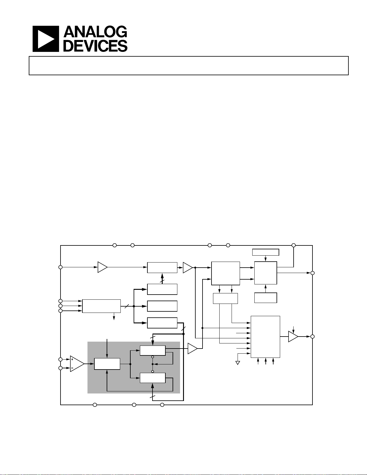
Charge Pump, PLL Synthesizer
ADF4113HV
GENERAL DESCRIPTION
The ADF4113HV is an integer-N frequency synthesizer with a
high voltage charge pump (15 V). The synthesizer is designed
for use with voltage controlled oscillators (VCOs) that have
high tuning voltages (up to 15 V). Active loop filters are often
used to achieve high tuning voltages, but the ADF4113HV
charge pump can drive a high voltage VCO directly with a
passive-loop filter. The ADF4113HV can be used to implement
local oscillators in the upconversion and downconversion
sections of wireless receivers and transmitters. It consists of a
low noise digital phase frequency detector (PFD), a precision
high voltage charge pump, a programmable reference divider,
programmable A and B counters, and a dual-modulus prescaler
(P/P + 1).
A simple 3-wire interface controls all of the on-chip registers.
The devices operate with a power supply ranging from 2.7 V to
5.5 V and can be powered down when not in use.
REF
CLK
DATA
RFINA
RF
IN
FUNCTIONAL BLOCK DIAGRAM
D
DD
IN
24-BIT
LE
B
INPUT REGISTER
SD
FROM
FUNCTION
LATCH
PRESCALER
P/P + 1
22
OUT
N=BP+A
R COUNTER
R COUNTER
FUNCTION
A, B COUNT ER
13-BIT
B COUNTER
LOAD
LOAD
6-BIT
A COUNTER
14-BIT
14
LATCH
LATCH
LATCH
19
13
P
CPGND
PHASE
FREQUENCY
DETECTOR
LOCK
DETECT
SD
AV
OUT
REFERENCE
CHARGE
PUMP
CURRENT
SETTING
DD
MUX
M3 M2 M1
ADF4113HV
6
R
SET
HIGH Z
CP
MUXOUT
CE AGND DGND
06223-001
Figure 1.
Rev. A
Information furnished by Analog Devices is believed to be accurate and reliable. However, no
responsibility is assumed by Analog Devices for its use, nor for any infringements of patents or other
rights of third parties that may result from its use. Specifications subject to change without notice. No
license is granted by implication or otherwise under any patent or patent rights of Analog Devices.
Trademarks and registered trademarks are the property of their respective owners.
One Technology Way, P.O. Box 9106, Norwood, MA 02062-9106, U.S.A.
Tel: 781.329.4700 www.analog.com
Fax: 781.461.3113 ©2007–2008 Analog Devices, Inc. All rights reserved.

ADF4113HV
TABLE OF CONTENTS
Features .............................................................................................. 1
Prescaler (P/P + 1) ........................................................................9
Applications ....................................................................................... 1
Functional Block Diagram .............................................................. 1
Revision History ............................................................................... 2
Specifications ..................................................................................... 3
Timing Characteristics ................................................................ 4
Absolute Maximum Ratings ............................................................ 5
Transistor Count ........................................................................... 5
Thermal Resistance ...................................................................... 5
ESD Caution .................................................................................. 5
Pin Configurations and Function Descriptions ........................... 6
Typical Performance Characteristics ............................................. 7
Circuit Description ........................................................................... 9
Reference Input Section ............................................................... 9
RF Input Stage ............................................................................... 9
A and B Counters ..........................................................................9
R Counter .......................................................................................9
Phase Frequency Detector (PFD) and Charge Pump ............ 10
Muxout and Lock Detect ........................................................... 10
Input Shift Register .................................................................... 10
Function Latch ............................................................................ 13
Applications ..................................................................................... 15
Using a Digitial-to-Analog Converter to Drive
the R
Pin .................................................................................. 15
SET
Interfacing ................................................................................... 15
PCB Design Guidelines for Chip Scale Package .................... 16
Outline Dimensions ....................................................................... 17
Ordering Guide .......................................................................... 17
REVISION HISTORY
9/08—Rev. 0 to Rev. A
Changes to Figure 22 ...................................................................... 13
1/07—Revision 0: Initial Version
Rev. A | Page 2 of 20

ADF4113HV
SPECIFICATIONS
AVDD = DVDD = 3 V ± 10%, 5 V ± 10%; 13.5 V < VP ≤ 16.5 V; AGND = DGND = CPGND = 0 V; R
T
= T
to T
A
MIN
, unless otherwise noted. Operating temperature range for B version: −40°C to +85°C.
MAX
Table 1.
1
Parameter B Version B Chips
Unit Test Conditions/Comments
RF CHARACTERISTICS (3 V)
RF Input Sensitivity −15/0 −15/0 dBm min/max
RF Input Frequency 0.2/3.7 0.2/3.7 GHz min/max For lower frequencies, ensure SR > 130 V/s
Prescaler Output Frequency
2
165 165 MHz max
RF CHARACTERISTICS (5 V)
RF Input Sensitivity −10/0 −10/0 dBm min/max
RF Input Frequency 0.2/3.7 0.2/3.7 GHz min/max For lower frequencies, ensure SR > 130 V/µs
0.2/4.0 0.2/4.0 GHz min/max Input level = −5 dBm
Prescaler Output Frequency 200 200 MHz max
REFIN CHARACTERISTICS
REFIN Input Frequency 5/150 5/150 MHz min/max For f < 5 MHz, ensure SR > 100 V/µs
Reference Input Sensitivity 0.4/AVDD 0.4/AVDD V p-p min/max AVDD = 3.3 V, biased at AVDD/2
1.0/AVDD 1.0/AVDD V p-p min/max For f ≥ 10 MHz, AVDD = 5 V, biased at AVDD/2
REFIN Input Capacitance 10 10 pF max
REFIN Input Current ±100 ±100 µA max
PHASE DETECTOR FREQUENCY 5 5 MHz max
CHARGE PUMP
I
Sink/Source R
CP
= 4.7 kΩ
SET
High Value 640 640 A typ
Low Value 80 80 µA typ
Absolute Accuracy 2.5 2.5 % typ
R
Range 3.9/10 3.9/10 kΩ typ
SET
ICP Three-State Leakage Current 5 5 nA max
Sink and Source Current Matching 3 3 % typ 1 V ≤ VCP ≤ VP – 1 V
ICP vs. VCP 1.5 1.5 % typ 1 V ≤ VCP ≤ VP – 1 V
ICP vs. Temperature 2 2 % typ VCP = VP/2
LOGIC INPUTS
V
, Input High Voltage 0.8 × DVDD 0.8 × DVDD V min
INH
V
, Input Low Voltage 0.2 × DVDD 0.2 × DVDD V max
INL
I
, Input Current ±1 ±1 µA max
INH/IINL
CIN, Input Capacitance 10 10 pF max
LOGIC OUTPUTS
VOH, Output High Voltage DVDD − 0.4 DVDD − 0.4 V min IOH = 500 µA
VOL, Output Low Voltage 0.4 0.4 V max IOL = 500 µA
POWER SUPPLIES
AVDD 2.7/5.5 2.7/5.5 V min/V max
DVDD AVDD AVDD
VP 13.5/16.5 13.5/16.5 V min/V max
5
I
(AIDD + DIDD) 16 11 mA max 11 mA typical
DD
IP 0.25 0.25 mA max TA = 25°C
Low Power Sleep Mode 1 1 µA typ
NOISE CHARACTERISTICS
= PN
− 10logf
TOT
6
−212 −212 dBc/Hz typ
− 20logN.
PFD
Normalized Phase Noise Floor
1
The B chip specifications are given as typical values.
2
This is the maximum operating frequency of the CMOS counters. The prescaler value should be chosen to ensure that the RF input is divided down to a frequency that
is less than this value.
3
AC coupling ensures AVDD/2 bias.
4
Guaranteed by characterization.
5
TA = 25oC; AVDD = DVDD = 5.5 V; P = 16; RFIN = 900 MHz.
6
The synthesizer phase noise floor is estimated by measuring the in-band phase noise at the output of the VCO, PN
value) and 10logf
: PN
PFD
SYNTH
= 4.7 kΩ; dBm referred to 50 Ω;
SET
3
, and subtracting 20logN (where N is the N divider
TOT
3, 4
Rev. A | Page 3 of 20
ADF4113HV
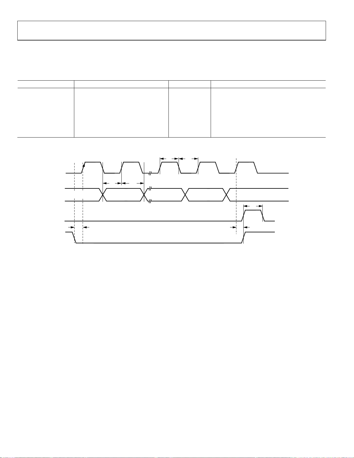
TIMING CHARACTERISTICS
Guaranteed by design but not production tested. AVDD = DVDD = 3 V ± 10%, 5 V ± 10%; 13.5 V ≤ VP ≤ 16.5 V;
AGND = DGND = CPGND = 0 V; R
Table 2.
Parameter Limit at T
t1 20 ns min LE setup time
t2 10 ns min DATA to CLK setup time
t3 10 ns min DATA to CLK hold time
t4 25 ns min CLK high duration
t5 25 ns min CLK low duration
t6 10 ns min CLK to LE setup time
t7 20 ns min LE pulse width
Timing Diagram
CLK
= 4.7 kΩ; TA = T
SET
to T
MIN
(B Version) Unit Test Conditions/Comments
MAX
MIN
to T
, unless otherwise noted.
MAX
t
4
t
5
DATA
t
2
DB23 (MSB) DB22 DB2
LE
t
1
LE
t
3
DB1
(CONTROL BIT C2)
DB0 (LSB)
(CONTROL BIT C1)
t
7
t
6
06223-002
Figure 2. Timing Diagram
Rev. A | Page 4 of 20
ADF4113HV
ABSOLUTE MAXIMUM RATINGS
TA = 25°C, unless otherwise noted.
Table 3.
Parameter Rating
AVDD to GND1 −0.3 V to +7 V
AVDD to DVDD −0.3 V to +0.3 V
VP to GND −0.3 V to +18 V
Digital I/O Voltage to GND −0.3 V to VDD + 0.3 V
Analog I/O Voltage to GND −0.3 V to VP + 0.3 V
REFIN, RFINA, RFINB to GND −0.3 V to VDD + 0.3 V
RFINA to RFINB ±320 mV
Operating Temperature Range
Industrial (B Version) −40°C to +85°C
Storage Temperature Range −65°C to +150°C
Maximum Junction Temperature 150°C
Lead Temperature, Soldering
Vapor Phase (60 sec) 215°C
Infrared (15 sec) 220°C
1
GND = AGND = DGND = 0 V.
Stresses above those listed under Absolute Maximum Ratings
may cause permanent damage to the device. This is a stress
rating only; functional operation of the device at these or any
other conditions above those indicated in the operational
section of this specification is not implied. Exposure to absolute
maximum rating conditions for extended periods may affect
device reliability.
TRANSISTOR COUNT
The transistor count is 12,150 (CMOS) and 348 (bipolar).
THERMAL RESISTANCE
Table 4. Thermal Resistance
Package Type θJA Unit
TSSOP 150.4 °C/W
LFCSP (Paddle Soldered) 122 °C/W
LFCSP (Paddle Not Soldered) 216 °C/W
ESD CAUTION
This device is a high performance RF integrated circuit with an
ESD rating of <1 kV, and it is ESD sensitive. Proper precautions
should be taken for handling and assembly.
Rev. A | Page 5 of 20
ADF4113HV
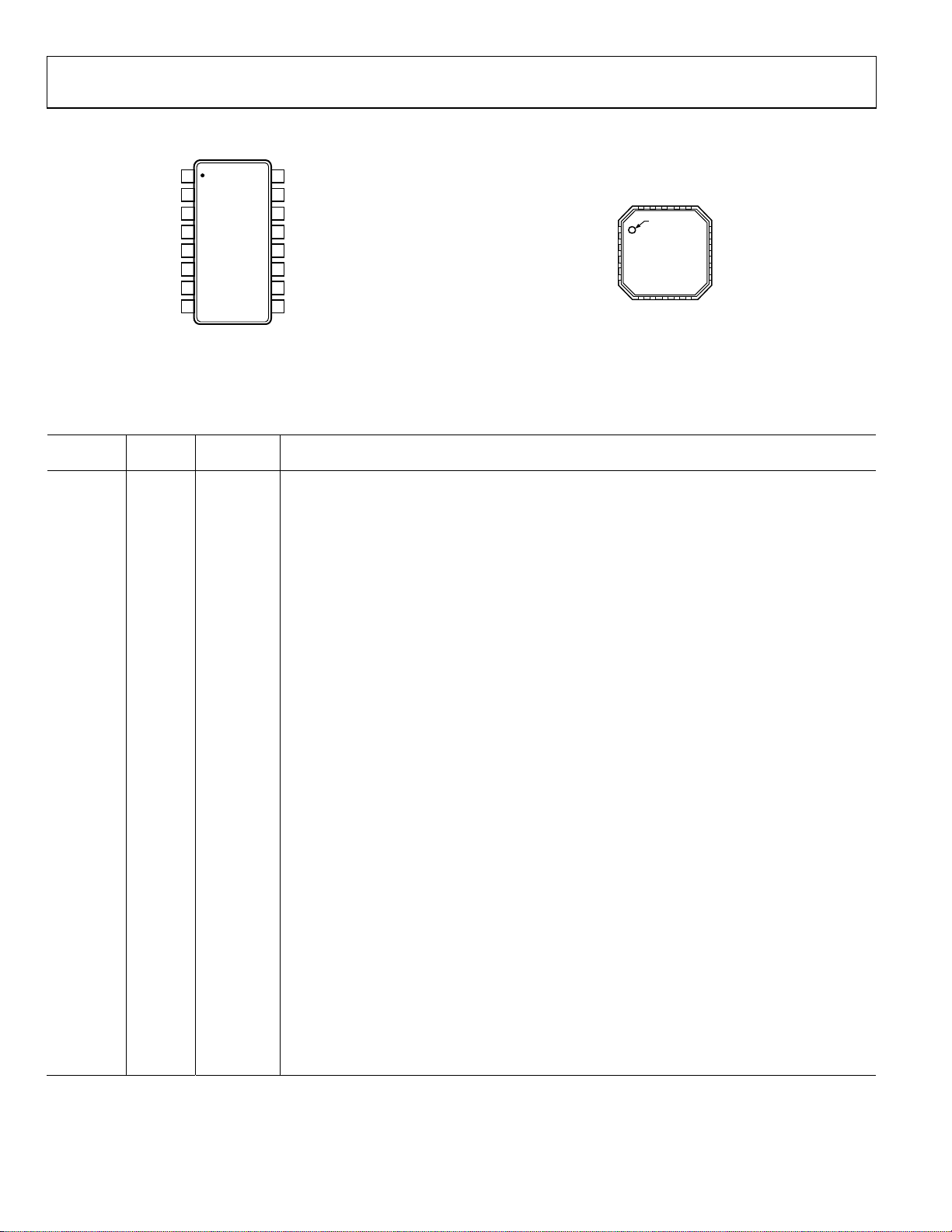
C
PIN CONFIGURATIONS AND FUNCTION DESCRIPTIONS
DD
DD
SET
1
R
SET
2
CP
3
PGND
AGND
R
R
AV
REF
FIN
FIN
B
A
DD
IN
ADF4113HV
TOP VIEW
4
(Not to Scale)
5
6
7
8
Figure 3. TSSOP Pin Configuration
16
15
14
13
12
11
10
9
V
P
DV
DD
MUXOUT
LE
DATA
CLK
CE
DGND
1CPGND
2AGND
3AGND
4RF
B
IN
5RF
A
IN
6223-003
Figure 4. LFCSP Pin Configuration
Table 5. Pin Function Descriptions
TSSOP
Pin No.
1 19 R
2 20 CP
LFCSP
Pin No. Mnemonic Description
SET
Connecting a resistor between this pin and CPGND sets the maximum charge pump output current.
The nominal voltage potential at the R
I
and R
SET
is I
CP
Charge Pump Output. When enabled, this pin provides ±I
CPmax
= 3/R
. Therefore, with R
SET
pin is 0.56 V for the ADF4113HV. The relationship between
SET
= 4.7 kΩ, I
SET
CPmax
CP
drives the external VCO.
3 1 CPGND Charge Pump Ground. CPGND is the ground return path for the charge pump.
4 2, 3 AGND Analog Ground. This is the ground return path of the prescaler.
5 4 RFINB
Complementary Input to the RF Prescaler. This point should be decoupled to the ground plane with
a small bypass capacitor, typically 100 pF.
6 5 RFINA Input to the RF Prescaler. This small-signal input is ac-coupled from the VCO.
7 6, 7 AVDD
Analog Power Supply. The power supply can range from 2.7 V to 5.5 V. Decoupling capacitors to the
analog ground plane should be placed as close as possible to this pin. AVDD must be the same value
.
as DV
DD
8 8 REFIN
Reference Input. This pin is a CMOS input with a nominal threshold of V
input resistance of 100 kΩ. This input can be driven from a TTL or CMOS crystal oscillator, or can be
ac-coupled.
9 9, 10 DGND Digital Ground.
10 11 CE
Chip Enable. A Logic low on this pin powers down the device and puts the charge pump output
into three-state mode. Taking the pin high powers up the device depending on the status of the
Power-Down Bit PD1.
11 12 CLK
Serial Clock Input. This serial clock is used to clock in the serial data to the registers. The data is
latched into the 24-bit shift register on the CLK rising edge. This input is a high impedance CMOS
input.
12 13 DATA
Serial Data Input. The serial data is loaded MSB first with the two LSBs being the control bits. This
input is a high impedance CMOS input.
13 14 LE
Load Enable, CMOS Input. When LE goes high, the data stored in the shift registers is loaded into
one of the four latches; the latch is selected using the control bits.
14 15 MUXOUT
Multiplexer Output. This multiplexer output allows either the lock detect, the scaled RF, or the
scaled reference frequency to be externally accessed.
15 16, 17 DVDD
Digital Power Supply. This can range from 2.7 V to 5.5 V. Decoupling capacitors to the digital ground
plane (1µF, 1nF) should be placed as close as possible to this pin. For best performance, the 1 µF
capacitor should be placed within 2 mm of the pin. The placing of the 1nF capacitor is less critical
16 18 VP
but should still be within 5 mm of the pin. DV
Charge Pump Power Supply. V
can range from 13.5 V to 16.5 V and should be decoupled
P
must have the same value as AVDD.
DD
appropriately.
P
DV
R
CP
DV
V
16
17
19
20
18
PIN 1
INDICATO R
ADF4113HV
TOP VIEW
(Not to Scale)
8
6
7
DD
DD
AV
AV
REF
15 MUXO UT
14 LE
13 DATA
12 CLK
11 CE
9
10
IN
DGND
DGND
= 640 A.
to the external loop filter; in turn, this
/2, and an equivalent
DD
06223-004
Rev. A | Page 6 of 20

ADF4113HV
–
–
TYPICAL PERFORMANCE CHARACTERISTICS
Loop bandwidth = 25 kHz, reference = 10 MHz reference from Agilent E4440A PSA, VCO = Sirenza VCO190-1500T(Y), evaluation
board = EVAL-ADF4113HVEBZ1.
FREQ
PARAM
–UNIT
–TYPE
GHz S MA R 50
FREQ MAGS11 ANGS11
0.05 0. 89207 –2.0571
0.10 0. 8886 –4.4427
0.15 0. 89022 –6.3212
0.20 0. 96323 –2.1393
0.25 0. 90566 –12.13
0.30 0. 90307 –13.52
0.35 0. 89318 –15.746
0.40 0. 89806 –18.056
0.45 0. 89565 –19.693
0.50 0. 88538 –22.246
0.55 0. 89699 –24.336
0.60 0. 89927 –25.948
0.65 0. 87797 –28.457
0.70 0. 90765 –29.735
0.75 0. 88526 –31.879
0.80 0. 81267 –32.681
0.85 0. 90357 –31.522
0.90 0. 92954 –34.222
0.95 0. 92087 –36.961
1.00 0. 93788 –39.343
DATA
–FORMAT
KEYWORD IMPEDANCE
FREQ MAGS11 ANGS11
1.05 0.9512 –40.134
1.10 0.93458 –43 .747
1.15 0.94782 –44 .393
1.20 0.96875 –46 .937
1.25 0.92216 –49 .6
1.30 0.93755 –51 .884
1.35 0.96178 –51 .21
1.40 0.94354 –53 .55
1.45 0.95189 –56 .786
1.50 0.97647 –58 .781
1.55 0.98619 –60 .545
1.60 0.95459 –61 .43
1.65 0.97945 –61 .241
1.70 0.98864 –64 .051
1.75 0.97399 –66 .19
1.80 0.97216 –63 .775
–OHMS
06223-005
Figure 5. S-Parameter Data for the ADF4113HV RF Input (Up to 1.8 GHz)
5
–5
–15
–25
–35
–45
–55
POWER (dB)
–65
–75
–85
–95
1.00G
0.25M
–1.25M
–1.00M
–0.75M
–0.50M
–0.25M
FREQUENCY (Hz)
0.50M
Figure 8. Reference Spurs (RF = 1000 MHz, PFD = 1 MHz)
1MHz
–92.428dBc
0.75M
1.00M
06223-043
1.25M
0
–5
–10
–15
–20
–25
–30
RF INPUT PO WER (dBm)
–35
–40
–45
06
1k 2k 3k 4k 5k
+85°C
+25°C
–40°C
RF INPUT FREQ UENCY (MHz)
06223-027
k
70
–80
–90
–100
–110
CARRIER POWER: –0.88dBm
–120
–130
–140
PHASE NOISE ( dBc/Hz)
–150
–160
–170
100 1M
Figure 6. Input Sensitivity
(RF = 1800 MHz, PFD= 1 MHz, V
70
–80
–90
–100
–110
CARRIER POWER: –5.09dBm
–120
–130
–140
PHASE NOISE ( dBc/Hz)
–150
–160
–170
100 1M
1kHz
–91.08dBc/Hz
1k 10k 100k
FREQUENCY OFFSET (Hz)
Figure 7. Integrated Phase Noise
(RF = 1000 MHz, PFD = 1 MHz, V
= 1.8 V, RMS Noise = 0.93°)
TUNE
06223-042
0
–10
–20
–30
–40
–50
–60
POWER (dB)
–70
–80
–90
–100
–1.25M
–1.00M
Figure 10. Reference Spurs (RF = 1800 MHz, PFD = 1 MHz)
Rev. A | Page 7 of 20
1kHz
–86.33dBc/Hz
1k 10k 100k
FREQUENCY OFFSET (Hz)
Figure 9. Integrated Phase Noise
= 13.1 V, RMS Noise = 1.16°)
TUNE
1.00G
–0.75M
–0.50M
–0.25M
FREQUENCY (Hz)
0.25M
1MHz
–87.264dBc
0.50M
0.75M
1.00M
06223-040
06223-041
1.25M

ADF4113HV
–
0
–20
–40
–60
–80
–100
FIRST REF ERENCE SPUR LEVEL (dBc)
–120
2468101214
01
TUNING VOL TAGE (V)
Figure 11. PFD Spurs (1 MHz) vs. V
50
–60
–70
TUNE
VDD = 3V
V
= 15V
P
06223-044
6
VDD = 3V
V
= 15V
P
800
600
400
200
0
–200
–400
CHARGE PUMP CURRENT (µ A)
–600
–800
01
1234567891011121314
VCP(V)
06223-026
5
Figure 13. Charge Pump Output Characteristics
PHASE NOISE (dBc/Hz)
–80
–90
–200 20406080
–40 100
TEMPERATURE ( °C)
06223-045
Figure 12. Phase Noise vs. Temperature
(RF = 1500 MHz, PFD = 1 MHz)
Rev. A | Page 8 of 20

ADF4113HV
CIRCUIT DESCRIPTION
REFERENCE INPUT SECTION
The reference input stage is shown in Figure 14. SW1 and SW2
are normally closed switches (NC in Figure 14). SW3 is normally
open (NO in Figure 14). When power-down is initiated, SW3 is
closed and SW1 and SW2 are opened. This ensures that there is
no loading of the REF
REF
IN
pin on power-down.
IN
POWER-DOW N
CONTROL
100kΩ
NC
NC
SW1
SW2
BUFFER
SW3
NO
Figure 14. Reference Input Stage
TO R COUNTER
06223-014
RF INPUT STAGE
The RF input stage is shown in Figure 15. It is followed by a
two-stage limiting amplifier to generate the current-mode logic
(CML) clock levels needed for the prescaler.
500Ω
1.6V
500Ω
AV
DD
RFINA
RF
IN
BIAS
GENERATOR
B
A AND B COUNTERS
The A and B CMOS counters combine with the dual-modulus
prescaler to allow a wide ranging division ratio in the PLL
feedback counter. The counters are specified to work when the
prescaler output is 200 MHz or less (for AV
with an RF input frequency of 2.5 GHz, a prescaler value of
16/17 is valid but a value of 8/9 is not.
Pulse Swallow Function
The A and B counters, in conjunction with the dual-modulus
prescaler, make it possible to generate output frequencies that
are spaced only by the reference frequency divided by R. The
equation for the VCO frequency is
f
= [(P × B) + A]f
VCO
REFIN
/R
where:
f
= output frequency of external voltage controlled
VCO
oscillator (VCO).
P = preset modulus of dual-modulus prescaler.
B = preset divide ratio of binary 13-bit counter (3 to 8191).
A = preset divide ratio of binary 6-bit swallow counter (0 to 63).
f
= output frequency of the external reference frequency
REFIN
oscillator.
R = preset divide ratio of binary 14-bit programmable reference
counter (1 to 16,383).
= 5 V). Thus,
DD
AGND
06223-015
Figure 15. RF Input Stage
PRESCALER (P/P + 1)
Together with the A and B counters, the dual-modulus prescaler
(P/P + 1) enables the large division ratio, N, to be realized by
N = BP + A
The dual-modulus prescaler, operating at CML levels, takes the
clock from the RF input stage and divides it down to a manageable
frequency for the CMOS A and CMOS B counters. The prescaler is programmable; it can be set in software to 8/9, 16/17,
32/33, or 64/65. It is based on a synchronous 4/5 core.
FROM RF
INPUT STAGE
N=BP+A
PRESCALER
MODULUS
CONTROL
P/P + 1
13-BIT B
COUNTER
LOAD
LOAD
6-BIT A
COUNTER
TO PFD
6223-016
Figure 16. A and B Counters
R COUNTER
The 14-bit R counter allows the input reference frequency to be
divided down to produce the reference clock to the phase frequency detector (PFD). Division ratios from 1 to 16,383 are
allowed.
Rev. A | Page 9 of 20

ADF4113HV
V
V
ANA
PHASE FREQUENCY DETECTOR (PFD) AND CHARGE PUMP
The PFD takes inputs from the R counter and N counter and
produces an output proportional to the phase and frequency
difference between them. Figure 17 is a simplified schematic.
The PFD includes a programmable delay element that controls
the width of the antibacklash pulse. This pulse ensures that
there is no dead zone in the PFD transfer function and minimizes phase noise and reference spurs. Two bits in the reference
counter latch, ABP2 and ABP1, control the width of the pulse.
See Figure 20. The only recommended setting for the antibacklash pulse width is 7.2 ns.
P
CHARGE
PUMP
UP
HIGH
R DIVIDER
HIGH
N DIVIDER
R DIVIDER
N DIVIDER
CP OUTPUT
Figure 17. PFD Simplified Schematic and Timing (in Lock)
Q1D1
U1
CLR1
PROGRAMMABLE
ABP1 ABP2
CLR2
Q2D2
U2
DELAY
DOWN
U3
CPGND
CP
MUXOUT AND LOCK DETECT
The output multiplexer on the ADF4113HV allows the user to
access various internal points on the chip. The state of MUXOUT
is controlled by M3, M2, and M1 in the function latch. Figure 22
shows the full truth table (function latch map). Figure 18 shows
the MUXOUT section in block diagram form.
D
DD
LOG LOCK DETECT
DIGITAL LOCK DETECT
R COUNTER OUTPUT
N COUNTER OUTPUT
SDOUT
CONTROLMUX
DGND
MUXOUT
06223-018
Figure 18. MUXOUT Circuit
Lock Detect
MUXOUT can be programmed for two types of lock detect:
digital lock detect and analog lock detect.
Digital lock detect is active high. When LDP in the AB counter
latch is set to 0, digital lock detect is set high when the phase
error on five consecutive phase detector (PD) cycles is less than
10 ns. With LDP set to 1, five consecutive cycles of less than
3 ns are required to set the lock detect. It stays high until a phase
error greater than 25 ns is detected on any subsequent PD cycle.
Operate the N-channel, open-drain, analog lock detect with a
10 kΩ nominal external pull-up resistor. When lock has been
detected, this output is high with narrow low-going pulses.
INPUT SHIFT REGISTER
The ADF4113HV digital section includes a 24-bit input shift
register, a 14-bit R counter, and a 19-bit N counter comprising
a 6-bit A counter and a 13-bit B counter. Data is clocked into
the 24-bit shift register on each rising edge of CLK, MSB first.
Data is transferred from the shift register to one of three latches
on the rising edge of LE. The destination latch is determined by
the state of the two control bits (C2, C1) in the shift register.
These are the two LSBs, DB1 and DB0, as shown in Figure 2.
6223-017
The truth table for these bits is shown in Tabl e 6. Figure 19
shows a summary of how the latches are programmed.
Table 6. C2, C1 Truth Table
Control Bits
C2 C1 Data Latch
0 0 R counter
0 1 N counter (A and B)
1 0 Function latch (including prescaler)
Rev. A | Page 10 of 20

ADF4113HV
Latch Summary
REFERENCE COUNTER LATCH
ANTI-
BACKLASH
RESERVED 14-BIT REFERE NCE COUNTER
DB23 DB22 DB21 DB20 DB19 DB18 DB17 DB16 DB15 DB14 DB13 DB12 DB11 DB10 DB9 DB8 DB7 DB6 DB5 DB4 DB3 DB2 DB1 DB0
000000ABP2ABP1R14R13R12R11R10R9R8R7R6R5R4R3R2R1C2(0)C1(0)
PULSE
WIDTH
N COUNTER LATCH
RE-
SERVEDLDPREC
DB23 DB22 DB21 DB20 DB19 DB18 DB17 DB16 DB15 DB14 DB13 DB12 DB11 DB10 DB9 DB8 DB7 DB6 DB5 DB4 DB3 DB2 DB1 DB0
0 L1 0 B13 B12 B11 B10 B9 B8 B7 B6 B5 B4 B3 B2 B1 A6 A5 A4 A3 A2 A1 C2(0) C1(1)
RE-
SERVED
13-BIT B COUNT ER 6-BIT A COUNTER
FUNCTION LATCH
CONTROL
BITS
CONTROL
BITS
PRE-
SCALER
VALUE RESERVED
DB23 DB22 DB21 DB20 DB19 DB18 DB17 DB16 DB15 DB14 DB13 DB12 DB11 DB10 DB9 DB8 DB7 DB6 DB5 DB4 DB3 DB2 DB1 DB0
P2P10000CP3CP2CP1000000F4F3M3M2M1F2F1C2(1)C1(0)
Reference Counter Latch Map
RESERVED
DB23 DB22 DB21 DB20 DB19 DB18 DB17 DB16 DB15 DB14 DB13 DB12 DB11 DB10 DB9 DB8 DB7 DB6 DB5 DB4 DB3 DB2 DB1 DB0
000000ABP2ABP1R14R13R12R11R10R9R8R7R6R5R4R3R2R1C2(0)C1(0)
THESE BITS MUST BE SET AS
INDICATED FOR NORMAL OPERATION
ABP2 ABP1
1 0 7.2ns (ONLY ALLOWED
CURRENT
SETTING RESERVED
ANTI-
BACKLASH
PULSE
WIDTH
ANTI-BACKLASH
PULSE WIDTH
SETTING)
CP THREE-
STATEPDPOLARITY
Figure 19. Latch Summary Tables
14-BIT REFERE NCE COUNTER
R14 R13 R12 .......... R3 R2 R1 DIVIDE RATIO
0 0 0 .......... 0 0 1 1
0 0 0 .......... 0 1 0 2
0 0 0 .......... 0 1 1 3
0 0 0 .......... 1 0 0 4
. . . .......... . . . .
. . . .......... . . . .
. . . .......... . . . .
1 1 1 .......... 1 0 0 16380
1 1 1 .......... 1 0 1 16381
1 1 1 .......... 1 1 0 16382
1 1 1 .......... 1 1 1 16383
Figure 20. Reference Counter Latch Bit Map
MUXOUT
CONTRO L
CONTROL
COUNTER
RESET
BITS
CONTROL
BITS
06223-019
06223-020
POWER
DOWN
Rev. A | Page 11 of 20

ADF4113HV
AB Counter Latch Map
RE-
SERVEDLDPREC
RE-
DB23 DB22 DB21 DB20 DB19 DB18 DB17 DB16 DB15 DB14 DB13 DB12 DB11 DB10 DB9 DB8 DB7 DB6 DB5 DB4 DB3 DB2 DB1 DB0
0 1 0 B13 B12 B11 B10 B9 B8 B7 B6 B5 B4 B3 B2 B1 A6 A5 A4 A3 A2 A1 C2(0) C1(1)
L2 LOCK DETECT PRECISION
0 10ns
13ns
SERVED
B13 B12 B11 B3 B2 B1 B COUNTER DIVIDE RATIO
0 0 0 .......... 0 0 0 NOT ALLOWED
0 0 0 .......... 0 0 1 NOT ALLOWED
0 0 0 .......... 0 1 0 NOT ALLOWED
0 0 0 .......... 1 1 1 3
. . . .... ...... . . . .
. . . .... ...... . . . .
. . . .... ...... . . . .
1 1 1 .......... 1 0 0 8188
1 1 1 .......... 1 0 1 8189
1 1 1 .......... 1 1 0 8190
1 1 1 .......... 1 1 1 8191
13-BIT B COUNT ER 6-BIT A COUNTER
A6 A5 A2 A1 A COUNTER DIVIDE RAT IO
0 0 .......... 0 0 0
0 0 .......... 0 1 1
0 0 .......... 0 0 2
0 0 .......... 1 1 3
. . .......... . . .
. . .......... . . .
. . .......... . . .
1 1 .......... 0 1 61
1 1 .......... 1 0 62
1 1 .......... 1 1 63
Figure 21. B Counter Latch Map
CONTRO L
BITS
06223-021
Rev. A | Page 12 of 20

ADF4113HV
Function Latch Map
PRE-
SCALER
VALUE RESERVED
DB23 DB22 DB21 DB20 DB19 DB18 DB17 DB16 DB15 DB14 DB13 DB12 DB11 DB10 DB9 DB8 DB7 DB6 DB5 DB4 DB3 DB2 DB1 DB0
P2P10000CP3CP2CP1000000F4F3M3M2M1F2F1C2(1)C1(0)
CPI3 CPI2 CPI1
00080
111640
P2 P1 PRESCALER VALUE
008/9
0116/17
1032/33
1164/65
CURRENT
SETTING RESERVED
ICP (µA)
4.7kΩ
F4
0NORMAL
1 THREE-STATE
CP THREE-
STATEPDPOLARITY
CHARGE PUMP
OUTPUT
PHASE DETECTO R
F3
POLARITY
1 POSITIVE
0NEGATIVE
M3 M2 M1 O UTPUT
0 0 0 THREE-ST ATE OUTPUT
0 0 1 DIGITAL LOCK DETECT
0 1 0 N DIVIDER O UTPUT
011DV
1 0 0 R DIVIDER O UTPUT
1 0 1 ANALOG L OCK DETECT
1 1 0 SERIAL DAT A OUTPUT
1 1 1 DGND
MUXOUT
CONTRO L
(ACTIVE HIG H)
DD
POWER
PD1 OPERATIO N
0NORMAL
1POWER DOWN
CONTRO L
DOWN
BITS
COUNTER
RESET
COUNTER
F1
OPERATION
0NORMAL
R, A, B COUNTERS
1
HELD IN RESET
Figure 22. Function Latch Map
06223-022
FUNCTION LATCH
The on-chip function latch is programmed with C2 and C1 set
to 1,0, respectively. Figure 22 shows the input data format for
programming the function latch.
Counter Reset
DB2 (F1) is the counter reset bit. When DB2 is 1, the R counter
and the AB counters are reset. For normal operation, this bit
should be 0. Upon powering up, the F1 bit must be disabled,
and the N counter resumes counting in close alignment with
the R counter. (The maximum error is one prescaler cycle.)
Power-Down
DB3 (F2) in the function latch provides a software power-down
for the ADF4113HV. The device powers down immediately
after latching a 1 into Bit F2.
When the CE pin is low, the device immediately powers down
regardless of the state of the power-down bit (F2).
When a power-down is activated (either through software or
a CE pin activated power-down), the following events occur:
• All active dc current paths are removed.
• The R, N, and timeout counters are forced to their load
state conditions.
• The charge pump is forced into three-state mode.
• The digital clock detect circuitry is reset.
Rev. A | Page 13 of 20
• The RF
A and RFINB inputs are debiased.
IN
• The reference input buffer circuitry is disabled.
• The input register remains active and capable of loading
and latching data.
MUXOUT Control
The on-chip multiplexer is controlled by M3, M2, and M1 on
the ADF4113HV. Figure 22 shows the truth table.
Charge Pump Currents
CPI3, CPI2, and CPI1 program the current setting for the
charge pump. The truth table is given in Figure 22.
Prescaler Value
P2 and P1 in the function latch set the prescaler values. The
prescaler value should be chosen so that the prescaler output
frequency is always less than or equal to 200 MHz. Thus, with
an RF frequency of 2 GHz, a prescaler value of 16/17 is valid,
but a value of 8/9 is not.
PD Polarity
This bit sets the phase detector polarity bit. See Figure 22.
CP Three-State
This bit controls the CP output pin. With the bit set high, the
CP output is put into three-state. With the bit set low, the CP
output is enabled.

ADF4113HV
DEVICE PROGRAMMING AFTER INITIAL
POWER-UP
After initial power-up of the device, there are two ways to
program the device.
CE Pin Method
1. Apply V
2. Bring CE low to put the device into power-down. This is an
asynchronous power-down in that it happens immediately.
3. Program the function latch (10). Program the R counter
latch (00). Program the AB counter latch (01).
4. Bring CE high to take the device out of power-down. The R
and AB counters resume counting in close alignment.
After CE goes high, a duration of 1 μs is sometimes required for
the prescaler band gap voltage and oscillator input buffer bias to
reach steady state.
CE can be used to power the device up and down to check for
channel activity. The input register does not need to be repro-
DD
.
grammed each time the device is disabled and enabled as long
as it has been programmed at least once after V
was initially
DD
applied.
Counter Reset Method
1. Apply V
DD
.
2. Conduct a function latch load (10 in 2 LSBs). As part of
this, load 1 to the F1 bit. This enables the counter reset.
3. Conduct an R counter load (00 in 2 LSBs).
4. Conduct an AB counter load (01 in 2 LSBs).
5. Conduct a function latch load (10 in 2 LSBs). As part of
this, load 0 to the F1 bit. This disables the counter reset.
This sequence provides the same close alignment as the initialization method. It offers direct control over the internal reset.
Note that counter reset holds the counters at load point and
three-states the charge pump, but does not trigger synchronous
power-down.
Rev. A | Page 14 of 20

ADF4113HV
APPLICATIONS
RF
OUT
100pF
2
FREF
8
IN
REF
CP
IN
ADF4113HV
CE
CLK
DATA
MUXOUT
LE
1
R
SET
12-BIT
RFINA
RF
IN
2.7kΩ
AD5320
V-OUT DAC
SPI-COMPAT IBLE SERIAL BUS
Figure 23. Driving the R
LOCK
14
DETECT
100pF
6
5
B
100pF
NOTES
1. POWE R SUPPLY CONNECTIONS AND DECOUPLING
CAPACITORS ARE O MITTED FOR CLARIT Y.
SET
USING A DIGITIAL-TO-ANALOG CONVERTER TO
DRIVE THE R
A digital-to-analog converter (DAC) can be used to drive the
pin of the ADF4113HV, thus increasing the level of control
R
SET
over the charge pump current (I
wideband applications where the sensitivity of the VCO varies
over the tuning range. To compensate for this, I
to maintain good phase margin and ensure loop stability. See
Figure 23 for this configuration.
SET
PIN
). This can be advantageous in
CP
can be varied
CP
INTERFACING
The ADF4113HV has a simple SPI®-compatible serial interface
for writing to the device. CLK, DATA, and LE control the data
transfer. When latch enable (LE) goes high, the 24 bits that have
been clocked into the input register on each rising edge of CLK
are transferred to the appropriate latch. See Figure 2 for the
timing diagram and Tabl e 6 for the latch truth table.
The maximum allowable serial clock rate is 20 MHz. This
means that the maximum update rate possible for the device
is 833 kHz, or one update every 1.2 μs. This rate is more than
adequate for systems that have typical lock times in the
hundreds of microseconds.
ADuC812 Interface
Figure 24 shows the interface between the ADF4113HV and the
ADuC812 MicroConverter®. Because the ADuC812 is based on
an 8051 core, this interface can be used with any 8051-based
Rev. A | Page 15 of 20
VCO
INPUT OUTPUT
GND
51Ω
LOOP
FILTER
Pin with a Digital-to-Analog Converter
microcontroller. The MicroConverter is set up for SPI master
mode with CPHA = 0. To initiate the operation, the I/O port
driving LE is brought low. Each latch of the ADF4113HV needs
a 24-bit word. This is accomplished by writing three 8-bit bytes
from the MicroConverter to the device. When the third byte
has been written, the LE input should be brought high to
complete the transfer.
I/O port lines on the ADuC812 are also used to control powerdown (CE input), and to detect lock (MUXOUT configured as
lock detect and polled by the port input).
When the ADuC812 is operating in the SPI master mode, the
maximum SCLOCK rate of the ADuC812 is 4 MHz. This
means that the maximum rate at which the output frequency
can be changed is 166 kHz.
SCLOCK
ADuC812
I/O PORTS
Figure 24. ADuC812 to ADF4113HV Interface
MOSI
100pF
18Ω
18Ω
18Ω
06223-023
CLK
DATA
LE
ADF4113HV
CE
MUXOUT
(LOCK DETECT)
06223-024

ADF4113HV
ADSP-21xx Interface
Figure 25 shows the interface between the ADF4113HV and the
ADSP-21xx digital signal processor. The ADF4113HV needs a
24-bit serial word for each latch write. The easiest way to
accomplish this using the ADSP-21xx family is to use the auto
buffered transmit mode of operation with alternate framing.
This provides a means for transmitting an entire block of serial
data before an interrupt is generated.
SCLK
ADSP-21xx
Figure 25. ADSP-21xx to ADF4113HV Interface
DT
TFS
I/O FLAGS
Set up the word length for eight bits and use three memory
locations for each 24-bit word. To program each 24-bit latch,
store the three 8-bit bytes, enable the auto buffered mode, and
then write to the transmit register of the DSP. This last operation initiates the autobuffer transfer.
CLK
DATA
ADF4113HV
LE
CE
MUXOUT
(LOCK DETECT)
06223-025
PCB DESIGN GUIDELINES FOR CHIP SCALE PACKAGE
The lands on the chip scale package (CP-20-1) are rectangular.
The printed circuit board pad for these should be 0.1 mm
longer than the package land length, and 0.05 mm wider than
the package land width. The land should be centered on the pad
to ensure that the solder joint size is maximized.
The bottom of the chip scale package has a central thermal pad.
The thermal pad on the printed circuit board should be at least
as large as this exposed pad. On the printed circuit board, provide
a clearance of at least 0.25 mm between the thermal pad and the
inner edges of the pad pattern. This ensures that shorting is
avoided.
Thermal vias can be used on the printed circuit board thermal
pad to improve thermal performance of the package. If vias are
used, they should be incorporated in the thermal pad at a 1.2 mm
pitch grid. The via diameter should be between 0.3 mm and
0.33 mm, and the via barrel should be plated with 1 oz. copper
to plug the via.
The user should connect the printed circuit board thermal pad
to AGND.
Rev. A | Page 16 of 20

ADF4113HV
R
OUTLINE DIMENSIONS
0.60
MAX
0.60
MAX
0.75
0.55
0.35
COPLANARITY
0.08
16
15
11
10
PIN 1
INDICATOR
20
1
5
6
0.30
0.23
0.18
2.25
2.10 SQ
1.95
0.25 MIN
PIN 1
INDICATO
1.00
0.85
0.80
SEATING
PLANE
12° MAX
BSC SQ
0.50
BSC
4.00
TOP
VIEW
0.80 MAX
0.65 TYP
0.20
REF
3.75
BCS SQ
0.05 MAX
0.02 NOM
COMPLIANT TO JEDEC STANDARDS MO-220-VGGD-1
Figure 26. 20-Lead Lead Frame Chip Scale Package [LFCSP_VQ]
4 mm x 4 mm Body, Very Thin Quad
(CP-20-1)
Dimensions shown in millimeters
5.10
5.00
4.90
0.15
0.05
4.50
4.40
4.30
PIN 1
16
0.65
BSC
COPLANARITY
COMPLIANT TO JEDEC STANDARDS MO-153-AB
0.10
0.30
0.19
9
81
1.20
MAX
SEATING
PLANE
6.40
BSC
0.20
0.09
8°
0°
0.75
0.60
0.45
Figure 27. 16-Lead Thin Shrink Small Outline Package [TSSOP]
(RU-16)
Dimensions shown in millimeters
ORDERING GUIDE
Model Temperature Range Package Description Package Option
ADF4113HVBRUZ
ADF4113HVBRUZ-RL
ADF4113HVBRUZ-RL7
ADF4113HVBCPZ
ADF4113HVBCPZ-RL
ADF4113HVBCPZ-RL7
EVAL-ADF4113HVEB1Z
1
Z = RoHS Compliant Part.
1
−40°C to +85°C 16-Lead Thin Shrink Small Outline Package [TSSOP] RU-16
1
−40°C to +85°C 16-Lead Thin Shrink Small Outline Package [TSSOP] RU-16
1
−40°C to +85°C 16-Lead Thin Shrink Small Outline Package [TSSOP] RU-16
1
−40°C to +85°C 20-Lead Lead Frame Chip Scale Package [LFCSP_VQ] CP-20-1
1
−40°C to +85°C 20-Lead Lead Frame Chip Scale Package [LFCSP_VQ] CP-20-1
1
−40°C to +85°C 20-Lead Lead Frame Chip Scale Package [LFCSP_VQ] CP-20-1
1
Evaluation Board
Rev. A | Page 17 of 20

ADF4113HV
NOTES
Rev. A | Page 18 of 20

ADF4113HV
NOTES
Rev. A | Page 19 of 20

ADF4113HV
NOTES
©2007–2008 Analog Devices, Inc. All rights reserved. Trademarks and
registered trademarks are the property of their respective owners.
D06223-0-9/08(A)
Rev. A | Page 20 of 20
 Loading...