

1750MHz Evaluation Board For PLL
=
FEATURES
Self-Contained Board including Synthesizer, VCO, Loop
Filter for generating frequencies of 1700MHz to
1800MHz
Designed for 20kHz Loop Bandwidth
Accompanying Software allows complete control of synthe-
sizer functions from PC
Battery Operated: Choice of 3V or 5V supplies
Typical Phase Noise Performance of -86dBc/Hz @ 1kHz
offset
BLOCK DIAGRAM
9V BATTERY
9V BATTERY
Frequency Synthesizer
EV AL-ADF4113EB2
GENERAL DESCRIPTION
This board is designed to allow the user to evaluate the
performance of the ADF4113 Frequency Synthesizer for
PLL's (Phase Locked Loops). The block diagram of the
board is shown below. It contains the ADF4113 synthesizer, a pc connector, SMA connector for the reference
input, power supplies and RF output. There is also a
loop filter (20kHz bandwidth) and a VCO on board. A
cable is included with the board to connect to a pc
printer port.
The package also contains windows software to allow
easy programming of the synthesizer.
V
V
DD
VCO
VCO 1
(Var i-L )
VCO 190-1750T
SMA
Socket
EVAL-ADF4113EB2
PC CONNECTOR
PC CONNECTOR
POWER SWITCH
ON OFF
ADF4 113
TCXO
TCXO
Vectron
AD7706
AD7706
V
P
CE
REF
IN
Information furnished by Analog Devices is believed to be accurate and reliable.
However, no responsibility is assumed by Analog Devices for its use, nor for any
infringements of patents or other rights of third parties which may result from its use.
No license is granted by implication or otherwise under any patent or patent rights of
Analog Devices.
REV.PrA 01/00
© Analog Devices, Inc., 1999
One Technology Way, P.O. Box 9106, Norwood, MA 02062-9106, U.S.A.
Tel: 781-329-4700 Fax: 781-326-8703
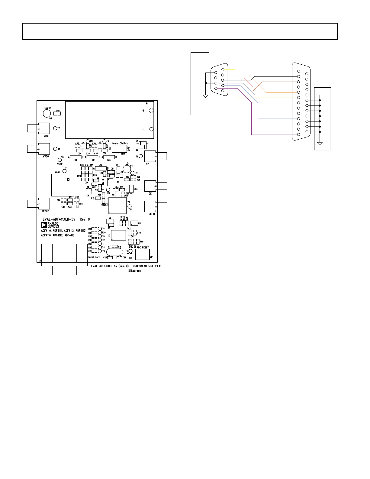
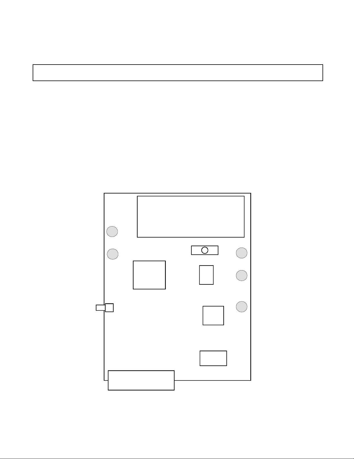
Hardware Description
The evaluation board comes with a cable for connecting to
the printer port of a PC. The silk screen and cable diagram for
the evaluation board are shown below. The board schematic is
shown on pages 3 and 4.
EV AL-ADF4113EB2
EVAL-ADF411X
EVAL-ADF421X
1
6
2
7
3
8
4
9
5
9 Way
Female D-Type
To
ADF411X
ADF421X
Evaluation
Board
Brown - DATA
Figure 2. PC Cable Diagram
Loop component values shown in the circuit diagram are
for 1750MHz RF output, 5mA CP current, VCO1901750T, 200kHz channel spacing and 20kHz loop bandwidth.
Black - CLK
Red - LE
Orange - CE
White - GND
Yellow
Blue
Purple
1
14
2
15
3
16
4
17
5
18
6
19
7
20
8
21
9
22
10
23
11
24
12
25
13
25 Way Male
D-Type
To
PC Printer Port
PC
Figure 1. Evaluation Board Silkscreen
The board is powered from a single 9V battery. The power
supply ciruitry allows the user to choose either 3V or 5V for
the ADF4113 V
default settings are 3V for the ADF4113 V
ADF4113 V
to note that the ADF4113 V
ADF4113 V
and VP, and for the VCO supply. The
DD
and for the VCO supply. It is very important
P
. This can damage the device.
P
should never exceed the
DD
and 5V for the
DD
All components necessary for LO generation are onboard. The 10 MHz TCXO from Vectron provides the
necessary Reference Input. The PLL is made up of the
ADF4113, passive loop filter (20kHz bandwidth) and the
VCO 190-1750 from Vari-L. The output is available at
RFOUT through a standard SMA connector. If the user
wishes they may use their own power supplies and reference input. In this case, they need to insert SMA connectors to as shown on the silkscreen and block diagram.
The AD7706 A/D converter is used to monitor the power
supply voltage and current consumption of the ADF4113.
This helps the user pick the optimum synthesizer settings for
power consumption and also provides an alert if the battery
voltage is too low to sustain the required 3V or 5V for the
board supply.
–2–
REV.PrA 01/00

EV AL-ADF4113EB2
Figure 3. Evaluation Board Circuit Diagram (Page 1)
–3–
REV.PrA 01/00

EV AL-ADF4113EB2
Figure 4. Evaluation Board Circuit Diagram (Page 2)
–4–
REV.PrA 01/00

Software Description
EV AL-ADF4113EB2
The software comes on a CD marked "ADF4xxx evaluation software". If the user double clicks on “setup.exe” on
the CD, then the install wizard installs the software. Follow the on-screen directions. The software will be installed in a default directory called
“C:\ProgramFiles\Analog Devices\ADF4XXX_rev0”.
The installation will create a shortcut under Analog Devices by default. The program can be run by clicking on
ADF4XXX_rev0.
On running the software a panel appears which asks the
user to choose the device to progam. Select the ADF4113.
The front panel will appear with some arbitrary values.
The evaluation board can be setup exactly by clicking
"Eval Board" near the top right corner of the panel. From
the following menu select ADF4113EB2.
This will program the device to the recommended settings
for the setup (i.e. charge pump current, prescaler, polarity
etc.) The user can adjust any of the settings by clicking
with the left mouse button on that feature and adjusting it
accordingly. The drop-down menus contain options to
examine the various test-modes or to set the configuration
options.
There is also a facility to monitor the Supply and Charge
Pump Voltage as well as the Device Current. To get the
most up to date reading just click on the "UpdateVoltage
and Current Display Button".
Figure 5. Software Front Panel
–5–
REV.PrA 01/00

EV AL-ADF4113EB2
Re ference Designat or De scri ption Ma nufactur er PCB DECAL VAL UE
Table 1. Bill of Materials for the EVAL-ADF4113EB2
U1 ADF4113BRU ADI TSSOP-16 ADF4113BRU
U2 AD7706BR ADI SO16WB AD7706BR
U3 AD780AR ADI SO8NB AD780AR
U4 ADP3300ART-5 ADI SOT23-6 ADP3300ART-5
U5 ADP3300ART-3 ADI SOT23-6 ADP3300ART-3
VCO1 VCO190-1750 Vari- L ( A ca l Elect . = Dis ti ) VCO190-1750
Y1 4.9152MHz Crystal
Y2 10 MHz TCXO
D1 SD103C Schottky Diode General Semiconductor DO35 SD103C
D2 IN4001 D035 FEC 365-117
D3 Red Low Power LED Visha LED FEC 657-130
D4 Green Low Power LED (Do Not Insert) Visha LED FEC 657-141
C1 C41 0.1uF Multi Layer Ceramic Capacitor Murata Case 0603 FEC 499-675
C2 10uF 6.3V Tantalum Capacitor AVX CAP\TAJ_B FEC 197-014
C3 C26 C27 C28 100pF Mul ti Layer Ceramic Capacitor Murata Case 0603 FEC 499-122
C4 C31 22uF 6.3V Tantalum Capacitor AVX CAP\TAJ_A FEC 197-038
C5 C7 C11 0.1uF Multi Layer Ceramic Capacitor Murata Case 0805 FEC 317-627
C6 C8 C9 C12 C3 10pF Multi Layer Ceramic Capacitor Murata Case 0603 FEC 499-110
C13 C14 1nF Multi Layer Ceramic Capacitor Murata Case 0603 FEC 317-202
C21 C22 33pF Multi Layer Ceramic Capacitor Murata Case 0603 FEC 498-555
C23 1nF Multi Layer Ceramic Capacitor Murata Case 0805
C24 10nF Multi Layer Ceramic Capacitor Murata Case 0805
C25 82pF Multi Layer Ceramic Capacitor Murata Case 0805
C33 C36 C40 10nF Multi Layer Ceramic Capacitor Murata Case 0603 FEC 499-146
C34 C37 1uF 16V Tantalum Capacitor AVX CAP\TAJ_A FEC 498-701
C35 C38 4.7uF 10V Tantalum Capacitor AVX CAP\TAJ_A FEC 498-658
C39 C42 10uF 6.3V Tantalum Capacitor AVX CAP\TAJ_A FEC 197-014
Ve ctro n Inter national
Ve ctro n Inter national
HC49 low profile VXA1-1011
T-118
R1 20r 5% Resistor (Surface Mount) Multicomp Case 0805 FEC 771-132
R2 R5 R6 R7 R8 R9 R10 330r 1% Resistor (Surface Mount) Multicomp Case 0603 FEC 911-143
R3 3k3 1% Resistor (Surface Mount) Multicomp Case 0603 FEC 911-290
R4 4k7 1% Resistor (Surface Mount) Multicomp Case 0603 FEC 911-318
R11 R25 Do Not Insert Case 0805
R18 1M 1% Resistor (Surface Mount) Multicomp Case 0603 FEC 911-598
R19 3k9 1% Resistor (Surface Mount) Case 0805
R20 20k 1% Resistor (Surface Mount) Case 0805
R21 R22 R23 18r 1% Resistor (Surface Mount) Multicomp Case 0603 FEC 911-021
R24 51r 1% Resistor (Surface Mount) Multicomp Case 0603
R27 R28 R29 10k 1% Resistor (Surface Mount) Multicomp Case 0603 FEC 911-355
R30 R31 R32 R33 R40 R41 100k 0.1% Resistor (Surface Mount) Meggitt Case 0603 FEC 911-471
R36 R37 330K 1% Res istor (Surface Mount) Multicomp Case 0603 FEC 911-537
R38 R39 0r 1% Resistor (Surface Mount) Multicomp Case 0603 FEC 772-227
R12 0r 1% Resistor - Do Not Insert Multicomp Case 0603 FEC 772-227
R42 4k7 1% Resistor (Surface Mount) Multicomp Case 0805 FEC 911-938
SW1 Push Button Switch Omron SW \PB-SMALL FEC 176-986
SW2 SPDT Switch - (Washable) Apem SW_SIP-3P FEC 150-559
T1-15 T19-21 Red Testpoint W Hughes TESTPOINT FEC-240-345
J1 9 PIN D-TYPE MALE (HORIZ) McMurdo DCON9M FEC 150-750
J2 J3 J4 J5 J6 Do Not Insert SMA
J7 GOLD 50Ω SMA SOCKET Pasterna SMA PE4118
LK1 LK4 LK5 3 pin header Harwin SIP-3P FEC 512-047
LK2-B Wire Lin
LK3 2 pin header Harwin SIP-2P FEC 512-035
LK1 LK3-5 Shorting Shunt Harwin FEC 150-410
P1 Pair PCB snap-on battery connector Keystone BATT_PP3 FEC 723-988
P1 9V PP3 Batter Duracell FEC 908-526
Each Corner Rubber Stick-On Feet 3M FEC 148-922
EVAL-ADF411XEB1 PCB ADI
Parts Free issued by ADI.
Leave position blank - Do not insert.
–6–
REV.PrA 01/00
 Loading...