

Page 1
V
A
Energy Metering IC with On-Chip Fault and
FEATURES
High accuracy, active energy measurement IC supports
IEC 62053-21
Less than 0.1% error over a dynamic range of 1000 to 1
Supplies active power on the frequency outputs, F1 and F2
High frequency output CF is intended for calibration and
supplies instantaneous active power
Continuous monitoring of the phase and neutral current
allows fault detection in 2-wire distribution systems
Current channel input level best suited for shunt and current
transformer sensors
Uses the larger of the two currents (phase or neutral) to bill,
even during a fault condition
Continuous monitoring of the voltage and current inputs
allows missing neutral detection
Uses one current input (phase or neutral) to bill when
missing neutral is detected
Two logic outputs (FAULT and REVP) can be used to indicate
a potential miswiring, fault, or missing neutral condition
Direct drive for electromechanical counters and 2-phase
stepper motors (F1 and F2)
Proprietary ADCs and DSP provide high accuracy over large
variations in environmental conditions and time
Reference 2.5 V ± 8% (drift 30 ppm/°C typical) with external
overdrive capability
Single 5 V supply, low power
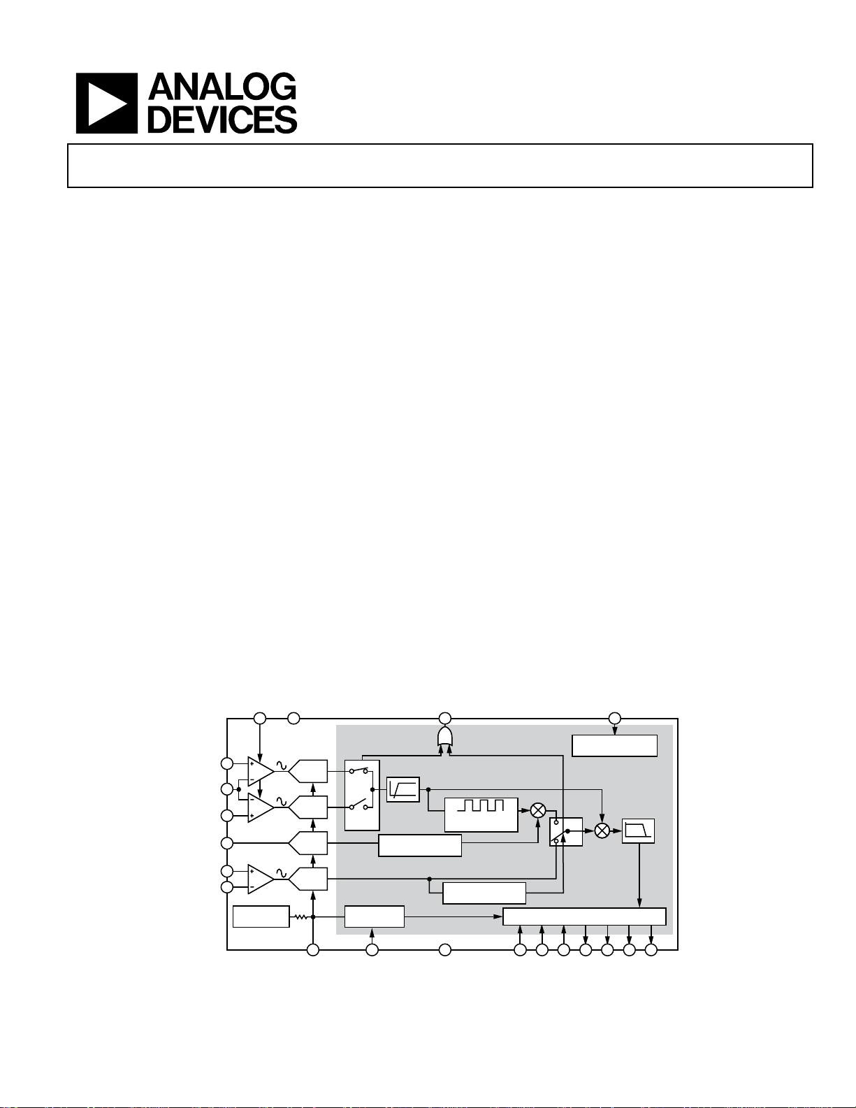
FUNCTIONAL BLOCK DIAGRAM
AGND FAULT
PG
13
V
2
V
V
MISCAL
V
V
1A
4
1N
3
1B
7
6
2P
5
2N
2.5V
REFERENCE
3kΩ
ADC
ADC
ADC
ADC
A > B
B > A
A ≠ B
MISSING NEUTRAL
INTERNAL
OSCILLATOR
HPF
GAIN ADJUST
Missing Neutral Detection
ADE7761B
GENERAL DESCRIPTION
The ADE7761B is a high accuracy, fault-tolerant, electrical energy
measurement IC intended for use with 2-wire distribution systems.
The part specifications surpass the accuracy requirements as
quoted in the IEC 62053-21 standard. The only analog circuitry
used on the ADE7761B is in the ADCs and reference circuit.
All other signal processing (such as multiplication and filtering)
is carried out in the digital domain. This approach provides
superior stability and accuracy over extremes in environmental
conditions and over time. The ADE7761B incorporates a fault
detection scheme similar to the
monitoring both phase and neutral currents. A fault is indicated
when the currents differ by more than 6.25%.
The ADE7761B incorporates a missing neutral detection scheme
by continuously monitoring the input voltage. When a missing
neutral condition is detected (no voltage input), the ADE7761B
continues billing based on the active current signal (see the
Missing Neutral Mode section). The missing neutral condition
is indicated when the FAULT pin goes high. The ADE7761B
supplies average active power information on the low frequency
outputs, F1 and F2. The CF logic output gives instantaneous
active power information.
The ADE7761B includes a power supply monitoring circuit on
the V
supply pin. Internal phase matching circuitry ensures
DD
that the voltage and current channels are matched. An internal
no-load threshold ensures that the ADE7761B does not exhibit
any creep when there is no load.
15 18
SUPPLY MONITOR
SIGNAL PROCESSING
ZERO-CROSSING
DETECTIO N
MISSING NE UTRAL
DETECTIO N
DIGITAL -TO-FREQUENCY CONVERT ER
ADE7751 by continuously
DD
POWER
ADE7761B
BLOCK
LPF
9 14 17 10 11 12
IN/OUT
16 18 19 20
F1F2CFREVPS0S1SCFDGNDRCLKINREF
06797-001
Figure 1.
Rev. 0
Information furnished by Analog Devices is believed to be accurate and reliable. However, no
responsibility is assumed by Anal og Devices for its use, nor for any infringements of patents or ot her
rights of third parties that may result from its use. Specifications subject to change without notice. No
license is granted by implication or otherwise under any patent or patent rights of Analog Devices.
Trademarks and registered trademarks are the property of their respective owners.
One Technology Way, P.O. Box 9106, Norwood, MA 02062-9106, U.S.A.
Tel: 781.329.4700 www.analog.com
Fax: 781.461.3113 ©2007 Analog Devices, Inc. All rights reserved.
Page 2

ADE7761B
TABLE OF CONTENTS
Features.............................................................................................. 1
General Description......................................................................... 1
Functional Block Diagram ..............................................................1
Revision History ...............................................................................2
Specifications..................................................................................... 3
Timing Characteristics ................................................................ 4
Absolute Maximum Ratings............................................................ 5
Performance Issues That May Affect Billing Accuracy........... 5
ESD Caution.................................................................................. 5
Pin Configuration and Function Descriptions............................. 6
Typical Performance Characteristics............................................. 8
Test Circuit ........................................................................................9
Terminology.................................................................................... 10
Theory of Operation ......................................................................11
Power Supply Monitor............................................................... 11
Analog Inputs .............................................................................11
Internal Oscillator...................................................................... 12
Analog-to-Digital Conversion.................................................. 13
Active Power Calculation.......................................................... 14
Digital-to-Frequency Conversion............................................ 16
Transfer Function....................................................................... 16
Fault Detection ...........................................................................17
Missing Neutral Mode............................................................... 18
Applications Information.............................................................. 21
Interfacing to a Microcontroller for Energy Measurement.. 21
Selecting a Frequency for an Energy Meter Application ......21
Negative Power Information..................................................... 22
Outline Dimensions....................................................................... 23
Ordering Guide .......................................................................... 23
REVISION HISTORY
8/07—Revision 0: Initial Version
Rev. 0 | Page 2 of 24
Page 3

ADE7761B
SPECIFICATIONS
VDD = 5 V ± 5%, AGND = DGND = 0 V, on-chip reference, on-chip oscillator, T
Table 1.
Parameter Value Unit Test Conditions/Comments
ACCURACY
Measurement Error
1
2
0.1 % of reading, typ Over a dynamic range of 1000 to 1
Phase Error Between Channels
PF = 0.8 Capacitive ±0.05 Degrees, max Phase lead 37°
PF = 0.5 Inductive ±0.05 Degrees, max Phase lag 60°
AC Power Supply Rejection
2
Output Frequency Variation 0.01 %, typ V1A = V1B = V2P = ±100 mV rms
DC Power Supply Rejection
2
Output Frequency Variation 0.01 %, typ V1A = V1B = V2P = ±100 mV rms
FAU LT D ETEC TION
2, 3
See the Fault Detection section
Fault Detection Threshold
Inactive Input ≠ Active Input 6.25 %, typ V1A or V1B active
Input Swap Threshold
Inactive Input ≠ Active Input 6.25 % of larger, typ V1A or V1B active
Accuracy Fault Mode Operation
V1A Active, V1B = AGND 0.1 % of reading, typ Over a dynamic range of 1000 to 1
V1B Active, V1A = AGND 0.1 % of reading, typ Over a dynamic range of 1000 to 1
Fault Detection Delay 3 Seconds, typ
Swap Delay 3 Seconds, typ
MISSING NEUTRAL MODE
2, 4
See the Missing Neutral Detection section
Missing Neutral Detection Threshold
V2P − V2N 59.4 mV peak, min
Accuracy Missing Neutral Mode
V1A Active, V1B = V2P = AGND 0.1 % of reading, typ Over a dynamic range of 500 to 1
V1B Active, V1A = V2P = AGND 0.1 % of reading, typ Over a dynamic range of 500 to 1
Missing Neutral Detection Delay 3 Seconds, typ
ANALOG INPUTS V1A − V1N, V1B − V1N, V2P − V2N
Maximum Signal Levels ±660 mV peak, max Differential input
660 mV peak, max Differential input MISCAL − V2N
Input Impedance (DC) 790 kΩ, min
Bandwidth (−3 dB) 7 kHz, typ
ADC Offset Error
2
15 mV, typ Uncalibrated error, see the Terminology section for details
Gain Error ±4 %, typ External 2.5 V reference
Gain Error Match
2
±3 %, typ External 2.5 V reference
REFERENCE INPUT
REF
Input Voltage Range 2.7 V, max 2.5 V + 8%
IN/OUT
2.3 V, min 2.5 V − 8%
Input Impedance 3 kΩ, min
Input Capacitance 10 pF, max
ON-CHIP REFERENCE
Reference Error ±200 mV, max
Temperature Coefficient 30 ppm/°C, typ
Current Source 10 µA, max Specification assures that V
ON-CHIP OSCILLATOR
Oscillator Frequency 450 kHz
Oscillator Frequency Tolerance ±12 % of reading, typ
Temperature Coefficient 30 ppm/°C, typ
MIN
to T
= −40°C to +85°C.
MAX
is within ±8%
REF
Specification achieved with 25 ppm/°C max resistor on the
RCLKIN pin
Rev. 0 | Page 3 of 24
Page 4
ADE7761B
Parameter Value Unit Test Conditions/Comments
LOGIC INPUTS
PGA, SCF, S1, and S0
Input High Voltage, V
Input Low Voltage, V
Input Current, IIN ±3 µA, max Typical 10 nA, VIN = 0 V to VDD
Input Capacitance, CIN 10 pF, max
LOGIC OUTPUTS
CF, REVP, and FAULT
Output High Voltage, VOH 4 V, min VDD = 5 V ± 5%
Output Low Voltage, VOH 1 V, max VDD = 5 V ± 5%
F1 and F2
Output High Voltage, VOH 4 V, min VDD = 5 V ± 5%, I
Output Low Voltage, VOH 1 V, max VDD = 5 V ± 5%, I
POWER SUPPLY For specified performance
VDD 4.75 V, min 5 V − 5%
5.25 V, max 5 V + 5%
IDD 3.65 mA, max
1
See plots in the Typical Performance Characteristics section.
2
See the Terminology section for explanation of specifications.
3
See the Fault Detection section for explanation of fault detection functionality.
4
See the Missing Neutral Detection section for explanation of missing neutral detection functionality.
5
Sample tested during initial release and after any redesign or process change that might affect this parameter.
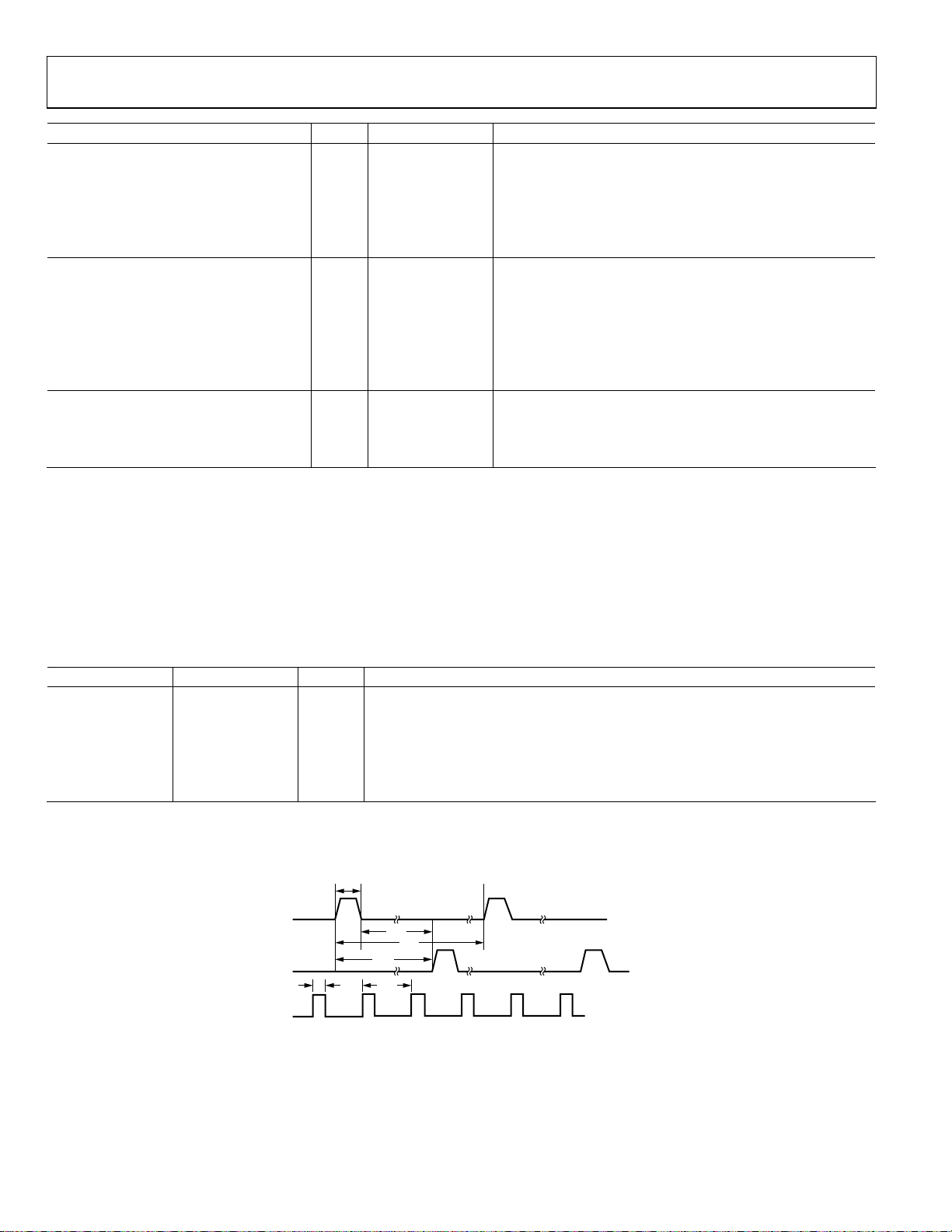
TIMING CHARACTERISTICS
VDD = 5 V ± 5%, AGND = DGND = 0 V, on-chip reference, on-chip oscillator, T
initial release and after any redesign or process change that might affect this parameter. See
5
2.4 V, min VDD = 5 V ± 5%
INH
0.8 V, max VDD = 5 V ± 5%
INL
5
to T
MIN
= 10 mA
SOURCE
= 10 mA
SINK
= −40°C to +85°C. Sample tested during
MAX
Figure 2.
Table 2.
Parameter Value Unit Test Conditions/Comments
1
t
1
120 ms F1 and F2 pulse width (logic high)
t2 See Table 8 sec Output pulse period (see the Transfer Function section)
t3 1/2 t2 sec Time between F1 falling edge and F2 falling edge
1
t
4
90 ms CF pulse width (logic high)
t5 See Table 8 sec CF pulse period (see the Transfer Function section)
t6 CLKIN/4 sec Minimum time between F1 pulse and F2 pulse
1
The pulse widths of F1, F2, and CF are not fixed for higher output frequencies. See the Transfer Function section.
Timing Diagram
t
1
F1
t
6
t
2
t
F2
t
4
CF
3
t
5
06797-002
Figure 2. Timing Diagram for Frequency Outputs
Rev. 0 | Page 4 of 24
Page 5
ADE7761B
ABSOLUTE MAXIMUM RATINGS
TA = 25°C, unless otherwise noted.
Table 3.
Parameter Rating
VDD to AGND −0.3 V to +7 V
Analog Input Voltage to AGND
V
, V1B, V1N, V2N, V2P, MISCAL
1A
Reference Input Voltage to AGND −0.3 V to VDD + 0.3 V
Digital Input Voltage to DGND −0.3 V to VDD + 0.3 V
Digital Output Voltage to DGND −0.3 V to VDD + 0.3 V
Operating Temperature Range
Industrial −40°C to +85°C
Storage Temperature Range −65°C to +150°C
Junction Temperature 150°C
20-Lead SSOP, Power Dissipation 450 mW
θJA Thermal Impedance 112°C/W
Lead Temperature, Soldering
Vapor Phase (60 sec) 215°C
Infrared (15 sec) 220°C
Stresses above those listed under Absolute Maximum Ratings
may cause permanent damage to the device. This is a stress
rating only; functional operation of the device at these or any
other conditions above those indicated in the operational
section of this specification is not implied. Exposure to absolute
maximum rating conditions for extended periods may affect
device reliability.
−6 V to +6 V
PERFORMANCE ISSUES THAT MAY AFFECT BILLING ACCURACY
The ADE7761B provides pulse outputs, CF, F1, and F2, that are
intended to be used for the billing of active energy. Pulses are
generated at these outputs in two different situations.
Case 1
When the analog input V2P − V2N complies with the conditions
described in
proportional to active power and can be used to bill active energy.
Case 2
When the analog input V2P − V2N does not comply with the
conditions described in
measure active energy but a quantity proportional to kiloamperehours (kAh). This quantity is used to generate pulses on the
same CF, F1, and F2. This situation is indicated when the
FAULT pin is high.
Analog Devices, Inc., cautions users of the ADE7761B about the
following:
• Billing active energy in Case 1 is consistent with the under-
standing of the quantity represented by pulses on the CF, F1,
and F2 outputs (watthour).
• Billing active energy while the ADE7761B is in Case 2 must
be decided knowing that the entity measured by the ADE7761B
in this case is ampere-hour and not watthour. Users should
be aware of this limitation and decide if the ADE7761B is
appropriate for their application.
Figure 34, the CF, F1, and F2 frequencies are
Figure 34, the ADE7761B does not
ESD CAUTION
Rev. 0 | Page 5 of 24
Page 6
ADE7761B
PIN CONFIGURATION AND FUNCTION DESCRIPTIONS
1
V
DD
2
V
1A
3
V
1B
V
4
1N
V
5
ADE7761B
MISCAL
REF
V
AGND
IN/OUT
SCF
2N
2P
6
7
8
9
10
TOP VIEW
(Not to Scale)
Figure 3. Pin Configuration (SSOP)
Table 4. Pin Function Descriptions
Pin No. Mnemonic Description
1 VDD
Power Supply. This pin provides the supply voltage for the digital circuitry in the ADE7761B. The supply voltage
should be maintained at 5 V ± 5% for specified operation. This pin should be decoupled with a 10 µF capacitor
in parallel with a ceramic 100 nF capacitor.
2, 3 V1A, V1B
Analog Inputs for Channel V1 (Current Channel). These inputs are fully differential voltage inputs with maximum
differential input signal levels of ±660 mV with respect to V
at these pins is ±1 V with respect to AGND. Both inputs have internal ESD protection circuitry, and an overvoltage
of ±6 V can also be sustained on these inputs without risk of permanent damage.
4 V1N
Negative Input for Differential Voltage Inputs, V
to AGND. The input has internal ESD protection circuitry, and an overvoltage of ±6 V can also be sustained on this
input without risk of permanent damage. The input should be directly connected to the burden resistor and held
5 V2N
at a fixed potential, that is, AGND. See the
Negative Input for Differential Voltage Inputs, V
Analog Inputs section.
respect to AGND. The input has internal ESD protection circuitry, and an overvoltage of ±6 V can also be sustained
on this input without risk of permanent damage. The input should be held at a fixed potential, that is, AGND. See
the
Analog Inputs section.
6 V2P
Analog Input for Channel V2 (Voltage Channel). This input is a fully differential voltage input with maximum
differential input signal levels of ±660 mV with respect to V
this pin is ±1 V with respect to AGND. This input has internal ESD protection circuitry, and an overvoltage of ±6 V
can also be sustained on this input without risk of permanent damage.
7 MISCAL
Analog Input for Missing Neutral Calibration. This pin can be used to calibrate the CF, F
missing neutral condition. This input is a fully differential voltage input with maximum differential input signal
levels of 660 mV with respect to V2N for specified operation. The maximum signal level at this pin is ±1 V with respect
to AGND. This input has internal ESD protection circuitry, and an overvoltage of ±6 V can also be sustained on this
input without risk of permanent damage.
8 AGND
Analog Ground. This pin provides the ground reference for the analog circuitry in the ADE7761B, that is, ADCs and
reference. This pin should be tied to the analog ground plane of the PCB. The analog ground plane is the ground
reference for all analog circuitry such as antialiasing filters and current and voltage transducers. For good noise
suppression, the analog ground plane should be connected to the digital ground plane only at the DGND pin.
9 REF
IN/OUT
This pin provides access to the on-chip voltage reference. The on-chip reference has a nominal value of
2.5 V ± 8% and a typical temperature coefficient of 30 ppm/°C. An external reference source can also be
connected at this pin. In either case, this pin should be decoupled to AGND with a 1 F ceramic capacitor and
100 nF ceramic capacitor.
10 SCF
Select Calibration Frequency. This logic input is used to select the frequency on the Calibration Output CF.
Table 7 shows how the calibration frequencies are selected.
11, 12 S1, S0
These logic inputs are used to select one of four possible frequencies for the digital-to-frequency conversion.
This offers the designer greater flexibility when designing the energy meter. See the
Energy Meter Application
section.
13 PGA This logic input is used to select the gain for the analog inputs, V1A and V1B. The possible gains are 1 and 16.
14 RCLKIN
To enable the internal oscillator as a clock source on the chip, a precise low temperature drift resistor at
a nominal value of 6.2 kΩ must be connected from this pin to DGND.
20
F1
19
F2
18
CF
17
DGND
16
REVP
15
FAULT
14
RCLKIN
13
PGA
12
S0
11
S1
and V1B. The maximum signal level at this pin is ±1 V with respect
1A
and MISCAL. The maximum signal level at this pin is ±1 V with
2P
06797-003
for specified operation. The maximum signal level
1N
for specified operation. The maximum signal level at
2N
, and F2 frequencies in the
1
Selecting a Frequency for an
Rev. 0 | Page 6 of 24
Page 7

ADE7761B
Pin No. Mnemonic Description
15 FAULT
16 REVP
17 DGND
18 CF
19, 20 F2, F1
This logic output goes active high when a fault or missing neutral condition occurs. A fault is defined as a
condition under which the signals on V
defined when the chip is powered up with no voltage at the input. The logic output is reset to 0 when a fault or
missing neutral condition is no longer detected. See the Fault Detection section and the Missing Neutral Mode
section.
This logic output goes logic high when negative power is detected, that is, when the phase angle between the
voltage and current signals is greater than 90°. This output is not latched and is reset when positive power is once
again detected. The output goes high or low at the same time that a pulse is issued on CF.
Digital Ground. This pin provides the ground reference for the digital circuitry in the ADE7761B, that is, multiplier,
filters, and digital-to-frequency converters. This pin should be tied to the digital ground plane of the PCB. The
digital ground plane is the ground reference for all digital circuitry, such as counters (mechanical and digital),
MCUs, and indicator LEDs. For good noise suppression, the analog ground plane should be connected to the digital
ground plane only at the DGND pin.
Calibration Frequency Logic Output. The CF logic output, active high, gives instantaneous active power information.
This output is used for operational and calibration purposes. See the
Low Frequency Logic Outputs. F1 and F2 supply average active power information. The logic outputs can be
used to directly drive electromechanical counters and 2-phase stepper motors.
and V1B differ by more than 6.25%. A missing neutral condition is
1A
Digital-to-Frequency Conversion section.
Rev. 0 | Page 7 of 24
Page 8
ADE7761B
TYPICAL PERFORMANCE CHARACTERISTICS
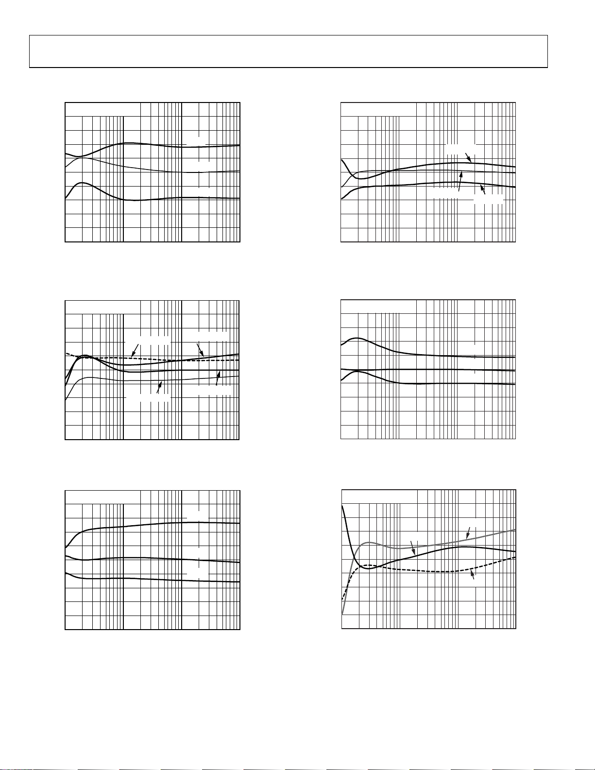
1.0
PF = 1
ON-CHIP REFE RENCE
0.8
0.6
0.4
0.2
0
–0.2
% ERROR
–0.4
–0.6
–0.8
–1.0
CURRENT (% of Fu ll Scale)
–40°C
+25°C
+85°C
06797-004
1000.1 1 10
Figure 4. Active Power Error As a Percentage of Reading
with Gain = 1 and Internal Reference
1.0
PF = 1
ON-CHIP REFE RENCE
0.8
0.6
0.4
0.2
0
–0.2
% ERROR
–0.4
–0.6
–0.8
–1.0
+85°C; PF = 0.5
+25°C; PF = 0.5
CURRENT (% of Fu ll Scale)
–40°C; PF = 0.5
+25°C; PF = 1
1000.1 1 10
06797-005
Figure 5. Active Power Error As a Percentage of Reading
over Power Factor with Gain = 1 and Internal Reference
1.0
PF = 1, GAIN = 16
ON-CHIP REFE RENCE
0.8
0.6
0.4
0.2
0
–0.2
% ERROR
–0.4
–0.6
–0.8
–1.0
CURRENT (% of Fu ll Scale)
–40°C
+25°C
+85°C
1000.1 1 10
06797-006
Figure 6. Active Power Error As a Percentage of Reading
with Gain = 16 and Internal Reference
1.0
GAIN = 16
ON-CHIP REFERENCE
0.8
0.6
0.4
0.2
0
–0.2
% ERROR
–0.4
–0.6
–0.8
–1.0
CURRENT (% of Fu ll Scale)
PF = –0.5
PF = +1
Figure 7. Active Power Error As a Percentage of Reading
over Power Factor with Gain = 16 and Internal Reference
1.0
GAIN = 16
ON-CHIP REFERENCE
0.8
0.6
0.4
0.2
0
–0.2
% ERROR
–0.4
–0.6
–0.8
–1.0
CURRENT (% of Fu ll Scale)
Figure 8. Active Power Error As a Percentage of Reading
over Power Supply with Gain = 1 and Internal Reference
1.0
ON-CHIP REFERE NCE
0.8
0.6
0.4
0.2
0
–0.2
% ERROR
–0.4
–0.6
–0.8
–1.0
–40°C
CURRENT (% of Full Scal e)
+25°C
+85°C
Figure 9. Ampere Hour Error As a Percentage of Reading
in Missing Neutral Mode with Gain = 1 and Internal Reference
5.25V
5.00V
4.75V
PF = +0.5
1000.1 1 10
06797-007
1000.1 1 10
6797-108
1000.1 1 10
06797-109
Rev. 0 | Page 8 of 24
Page 9

ADE7761B
V
V
TEST CIRCUIT
DD
+
220
40A TO 80mA
RB = 18Ω
1MΩ
10µF
I
RB
RB
33nF1kΩ
560kΩ
100kΩ
1kΩ
33nF
1kΩ
33nF
1kΩ
33nF
1kΩ
33nF
33nF
100nF
2
3
4
5
6
7
1
V
DD
V
1A
V
1B
V
1N
V
2N
V
2P
MISCAL
ADE7761B
AGND DGNDPGA
RCLKIN
REF
REVP
FAULT
SCF
IN/OUT
1713 8
10kΩ
100nF
PS2501-1
1
2
4
3
+
TO FREQ.
COUNTER
10µF
2kΩ
18
CF
19
F2
20
F1
16
2kΩ
15
6.2kΩ
14
12
S0
11
S1
10
9
06797-008
Figure 10. Test Circuit for Performance Curves
Rev. 0 | Page 9 of 24
Page 10

ADE7761B
r
e
TERMINOLOGY
Measurement Error
The error associated with the energy measurement made by the
ADE7761B is defined by
=
Percentag
⎛
⎜
⎜
⎝
Phase Error Between Channels
The high-pass filter (HPF) in the current channel has a phase
lead response. To offset this phase response and equalize the
phase response among channels, a phase correction network is
also placed in the current channel. The phase correction network
ensures a phase match between the current channels and the
voltage channels to within ±0.1° over a range of 45 Hz to
65 Hz and ±0.2° over a range of 40 Hz to 1 kHz.
Power Supply Rejection (PSR)
PSR quantifies the ADE7761B measurement error as a percentage
of reading when the power supplies are varied. For the ac PSR
measurement, a reading at nominal supplies (5 V) is taken.
A second reading is obtained with the same input signal levels
when an ac signal (175 mV rms/100 Hz) is introduced onto the
supplies. Any error introduced by this ac signal is expressed as
a percentage of reading (see the Measurement Error definition).
Erro
−
EnergyTrueADE7761BbyRegisteredEnergy
EnergyTrue
⎞
⎟
%100×
⎟
⎠
For the dc PSR measurement, a reading at nominal supplies (5 V)
is taken. A second reading is obtained with the same input signal
levels when the power supplies are varied ±5%. Any error
introduced is again expressed as a percentage of reading.
ADC Offset Error
This is the dc offset associated with the analog inputs to the ADCs.
With the analog inputs connected to AGND, the ADCs still see
a dc analog input signal. The magnitude of the offset depends on
the input gain and range selection (see the
Characteristics
the offset is removed from the current channels and the power
calculation is not affected by this offset.
Gain Error
The gain error in the ADE7761B ADCs is defined as the difference
between the measured output frequency (minus the offset) and
the ideal output frequency. It is measured with a gain of 1 in
Channel V
ideal frequency, which is obtained from the transfer function
(see the
Gain Error Match
The gain error match is defined as the gain error (minus the offset)
obtained when switching between a gain of 1 or 16. It is expressed
as a percentage of the output ADC code obtained under a gain of 1.
section). However, when HPFs are switched on,
. The difference is expressed as a percentage of the
1A
Transfer Funct ion section).
Typical Performanc e
Rev. 0 | Page 10 of 24
Page 11
ADE7761B
V
V
V
THEORY OF OPERATION
POWER SUPPLY MONITOR
The ADE7761B continuously monitors the power supply (VDD)
with its on-chip power supply monitor. If the supply is less than
4 V ± 5%, the ADE7761B goes into an inactive state; that is, no
energy is accumulated, and the CF, F1, and F2 outputs are disabled.
This is useful to ensure correct device operation at power-up
and during power-down. The power supply monitor has built-in
hysteresis and filtering that provide a high degree of immunity
to false triggering due to noisy supplies.
The power supply and decoupling for the part should be such
that the ripple at V
does not exceed 5 V ± 5%, as specified for
DD
normal operation.
DD
5V
4V
0V
ADE7761B
REVP - FAULT - CF -
F1 - F2 OUTPUTS
INACTIVE ACTIVE
Figure 11. On-Chip, Power Supply Monitoring
TIME
INACTIVE
ANALOG INPUTS
Channel V1 (Current Channel)
The voltage outputs from the current transducers are connected
to the ADE7761B at Channel V1. It has two voltage inputs, V
. These inputs are fully differential with respect to V1N.
and V
1B
However, at any one time, only one input is selected to perform
the power calculation (see the
The maximum peak differential signal on V
Fault Detection section).
− V1N and V1B − V1N
1A
is ±660 mV. However, Channel V1 has a programmable gain
amplifier (PGA) with user-selectable gains of 1 and 16 (see
Table 5). This gain facilitates easy transducer interfacing.
Table 5. Channel V1 Dynamic Range
PGA Gain Maximum Differential Signal (mV)
0 1 660
1 16 41
Figure 12 shows the maximum signal levels on V1A, V1B, and
. The maximum differential voltage is ±660 mV divided by
V
1N
the gain selection. The differential voltage signal on the inputs
must be referenced to a common mode (usually AGND).
1A
DIFFERENTIAL INPUT A
±660mV MAX PEAK
COMMON MODE
±100mV MAX
DIFFERENTIAL INPUT B
±660mV MAX PEAK V
AGND
V
CM
+660mV
GAIN
–660mV
GAIN
+ V
+ V
, V
V
1A
1B
CM
V
CM
CM
Figure 12. Maximum Signal Levels, Channel V1
Channel V2 (Voltage Channel)
The output of the line voltage transducer is connected to the
ADE7761B at this analog input. Channel V2 is a single-ended
voltage input. The maximum peak differential signal on
Channel V2 is ±660 mV with respect to V
. Figure 13 shows the
2N
maximum signal levels that can be connected to Channel V2.
+660mV + V
–660mV + V
06797-009
2
CM
V
CM
CM
DIFFERENTIAL INPUT
±660mV MAX PEAK
COMMON MODE
±100mV MAX
Figure 13. Maximum Signal Levels, Channel V2
The differential voltage V2P − V2N must be referenced to a
common mode (usually AGND). The analog inputs of the
ADE7761B can be driven with common-mode voltages of up
to 100 mV with respect to AGND. However, the best results
are achieved using a common mode equal to AGND.
MISCAL Input
The input for the power calibration in missing neutral mode
is connected to the ADE7761B at this analog input. MISCAL
is a single-ended, voltage input. It is recommended to use a dc
signal derived from the voltage reference to drive this pin. The
maximum peak differential signal on MISCAL is 660 mV with
respect to V
. Figure 14 shows the maximum signal levels that
2N
can be connected to the MISCAL pin.
MISCAL
+660mV + V
CM
V
CM
DIFFERENTIAL INPUT
±660mV MAX PEAK
COMMON MODE
±100mV MAX
Figure 14. Maximum Signal Levels, MISCAL
The differential voltage, MISCAL − V2N, must be referenced
to a common mode (usually AGND). The analog inputs of the
ADE7761B can be driven with common-mode voltages of up to
100 mV with respect to AGND. However, best results are achieved
using a common mode equal to AGND.
V1
V
V1
V
V2
V
V
CM
MISCAL
MISCAL
V
V
CM
AGND
1A
1N
1B
2P
2N
2N
06797-010
06797-011
06797-012
Rev. 0 | Page 11 of 24
Page 12
ADE7761B
V
V
A
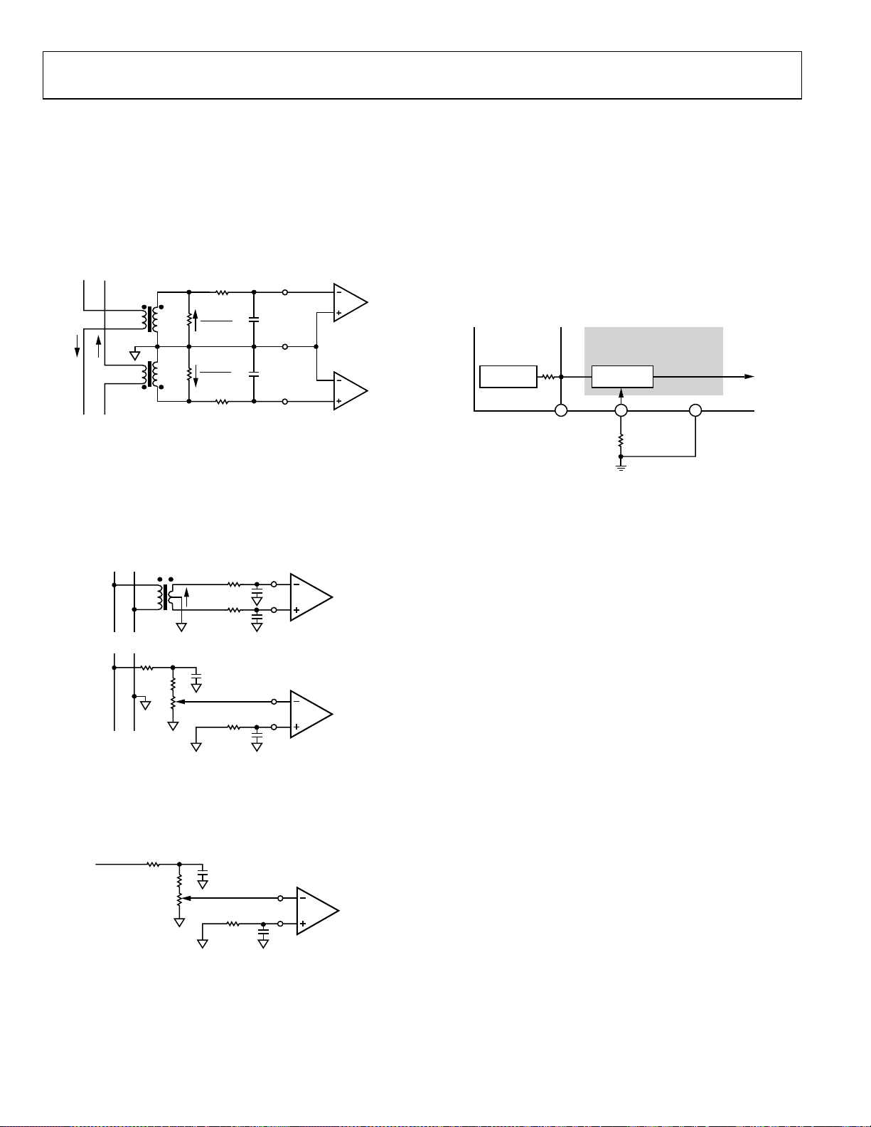
Typical Connection Diagrams
Figure 15 shows a typical connection diagram for Channel V1.
The analog inputs are used to monitor both the phase and
neutral currents. Because of the large potential difference
between the phase and neutral, two current transformers (CTs)
must be used to provide the isolation. Note that both CTs are
referenced to analog ground (AGND); therefore, the commonmode voltage is 0 V. The CT turn ratio and burden resistor (RB)
are selected to give a peak differential voltage of ±660 mV/gain.
R
±660mV
GAIN
±660mV
GAIN
R
F
F
CT
RB
INIP
AGND
RB
PHASE
CT
NEUTRAL
Figure 15. Typical Connection for Channel V1
1A
C
F
V
1N
C
F
V
1B
6797-013
Figure 16 shows two typical connections for Channel V2.
The first option uses a potential transformer (PT) to provide
complete isolation from the main voltage. In the second option,
the ADE7761B is biased around the neutral wire, and a resistor
divider is used to provide a voltage signal that is proportional to
the line voltage. Adjusting the ratio of RA and RB + VR is a
convenient way to carry out a gain calibration on the meter.
R
±660mV
R
NEUTRAL
PHASE
RA
NEUTRAL
PHASE
1
RB + VR = RF.
AGND
1
C
RB
VR
1
1
F
Figure 16. Typical Connections for Channel V2
2P
F
C
F
V
2N
F
C
F
V
2P
V
R
2N
F
C
T
06797-014
Figure 17 shows a typical connection for the MISCAL input.
The voltage reference input (REF
) is used as a dc reference
IN/OUT
to set the MISCAL voltage.
REF
RC
IN/OUT
C
RD
VR1
F
MISCAL
R
F
C
F
Figure 17. Typical Connection for MISCAL
V
2N
06797-015
Adjusting the level of MISCAL to calibrate the meter in missing
neutral mode can be done by changing the ratio of RC and
RD + VR1. When the internal reference is used, the values of RC,
RD, and VR1 must be chosen to limit the current sourced by
the internal reference sourcing current to below the specified
10 μA. Therefore, because V
internal = 2.5 V, RC + RD +
REF
VR1 > 600 kΩ.
INTERNAL OSCILLATOR
The nominal internal oscillator frequency is 450 kHz when
used with the recommended R
between RCLKIN and DGND (see
DE7761B
3kΩ
2.5V
REFERENCE
9
IN/OUT
Figure 18. Internal Oscillator Connection
The internal oscillator frequency is inversely proportional to the
value of this resistor. Although the internal oscillator operates
when used with an R
resistor value between 5 kΩ and 12 kΩ,
OSC
it is recommended that a value be chosen within the range of
the nominal value.
The output frequencies on CF, F1, and F2 are directly proportional to the internal oscillator frequency; therefore, Resistor R
must have a low tolerance and low temperature drift. A low
tolerance resistor limits the variation of the internal oscillator
frequency. A small variation of the clock frequency and, consequently, of the output frequencies from meter to meter contributes
to a smaller calibration range of the meter.
A low temperature drift resistor directly limits the variation of
the internal clock frequency over temperature. The stability of
the meter to external variation is then better ensured by design.
resistor value of 6.2 kΩ
OSC
Figure 18).
INTERNAL
OSCILLAT OR
14 17
R
OSC
DGNDRCLKINREF
06797-016
OSC
Rev. 0 | Page 12 of 24
Page 13

ADE7761B
S
S
A
A
ANALOG-TO-DIGITAL CONVERSION
The analog-to-digital conversion in the ADE7761B is carried
out using second-order, Σ-Δ ADCs.
order, Σ-Δ ADC (for simplicity). The converter is made up of
two parts: the Σ-Δ modulator and the digital low-pass filter.
ANALOG
LOW-PASS FILTER
R
C
INTEGRATOR
V
REF
Figure 19. First-Order, Σ-Δ ADC
A Σ-Δ modulator converts the input signal into a continuous
serial stream of 1s and 0s at a rate determined by the sampling
clock. In the ADE7761B, the sampling clock is equal to CLKIN.
The 1-bit DAC in the feedback loop is driven by the serial data
stream. The DAC output is subtracted from the input signal.
If the loop gain is high enough, the average value of the DAC
output (and, therefore, the bit stream) approaches that of the
input signal level. For any given input value in a single sampling
interval, the data from the 1-bit ADC is virtually meaningless.
Only when a large number of samples are averaged is a meaningful
result obtained. This averaging is carried out in the second part
of the ADC, the digital low-pass filter. By averaging a large
number of bits from the modulator, the low-pass filter can
produce 24-bit data-words that are proportional to the input
signal level.
The Σ-Δ converter uses two techniques to achieve high resolution
from what is essentially a 1-bit conversion technique. The first is
oversampling, which means that the signal is sampled at a rate
(frequency) that is many times higher than the bandwidth of
interest. For example, the sampling rate in the ADE7761B is
CLKIN (450 kHz) and the band of interest is 40 Hz to 1 kHz.
Oversampling has the effect of spreading the quantization noise
(noise due to sampling) over a wider bandwidth. With the noise
spread more thinly over a wider bandwidth, the quantization
noise in the band of interest is lowered (see
However, oversampling alone is not an efficient enough method
to improve the signal-to-noise ratio (SNR) in the band of interest.
For example, an oversampling ratio of 4 is required just to increase
the SNR by only 6 dB (1 bit). To keep the oversampling ratio at
a reasonable level, it is possible to shape the quantization noise so
the majority of the noise lies at the higher frequencies. This is what
happens in the Σ-Δ modulator; the noise is shaped by the integrator, which has a high-pass type response for the quantization
noise. The result is that most of the noise is at higher frequencies,
where it can be removed by the digital low-pass filter. This noise
shaping is also shown in
Figure 20.
Figure 19 shows a first-
MCLK
LATCHED
COMPARATOR
....10100101....
1-BIT DAC
Figure 20).
DIGITAL
LOW-PASS FILTER
1 24
NTIALIAS FILTER (RC)
IGNAL
NOISE
0 1 225 450
IGNAL
NOISE
06797-017
0 1 225 450
DIGITAL FILTER
FREQUENCY (kHz)
HIGH RESOL UTION
OUTPUT FROM
DIGITAL LFP
FREQUENCY (kHz)
Figure 20. Noise Reduction Due to Oversampling and
Noise Shaping in the Analog Modulator
SAMPLING F REQUENCY
SHAPED NOISE
06797-018
Antialias Filter
Figure 20 also shows an analog low-pass filter, RC, on input to
the modulator. This filter is present to prevent aliasing. Aliasing
is an artifact of all sampled systems, which means that frequency
components in the input signal to the ADC that are higher than
half the sampling rate of the ADC appear in the sampled signal
frequency below half the sampling rate.
Figure 21 illustrates
the effect.
NTIALIASING EFF ECTS
SAMPLING
IMAGE
FREQUENCIES
0 1 225 450
FREQUENCY (kHz)
Figure 21. ADC and Signal Processing in Current Channel or Voltage Channel
FREQUENCY
06797-019
In Figure 21, frequency components (arrows shown in black)
above half the sampling frequency (also known as the Nyquist
frequency), that is, 225 kHz, are imaged or folded back down
below 225 kHz (arrows shown in gray). This happens with all
ADCs, no matter what the architecture. In
Figure 21, only
frequencies near the sampling frequency (450 kHz) move into
the band of interest for metering (40 Hz to 1 kHz). This fact
allows the use of a very simple low-pass filter to attenuate these
frequencies (near 250 kHz) and, thereby, prevent distortion in the
band of interest. A simple RC filter (single pole) with a corner
frequency of 10 kHz produces an attenuation of approximately
33 dB at 450 kHz (see
Figure 21). This is sufficient to eliminate
the effects of aliasing.
Rev. 0 | Page 13 of 24
Page 14

ADE7761B
ACTIVE POWER CALCULATION
The ADCs digitize the voltage signals from the current and
voltage transducers. A high-pass filter in the current channel
removes any dc component from the current signal. This eliminates
any inaccuracies in the active power calculation due to offsets in
the voltage or current signals (see the
section).
The active power calculation is derived from the instantaneous
power signal. The instantaneous power signal is generated by
a direct multiplication of the current and voltage signals.
To extract the active power component (dc component), the
instantaneous power signal is low-pass filtered.
the instantaneous active power signal and shows how the active
power information can be extracted by low-pass filtering the
instantaneous power signal. This scheme correctly calculates
active power for nonsinusoidal current and voltage waveforms
at all power factors. All signal processing is carried out in the
digital domain for superior stability over temperature and time.
CH1
CH2
V × I
PGA
TIME
ADC
HPF
MULTIPLIER
ADC
INSTANTANEO US
POWER SIG NAL –p(t)
p(t) = i(t) × v(t)
WHERE:
v(t) = V × cos(ωt)
i(t) = I × cos(ωt)
V × I
p(t) =
{1 + cos (2ωt)}
2
Figure 22. Signal Processing Block Diagram
The low frequency output of the ADE7761B is generated by
accumulating this active power information. This low frequency
inherently means a long accumulation time between output
pulses. The output frequency is, therefore, proportional to the
average active power. This average active power information
can, in turn, be accumulated (for example, by a counter) to
generate active energy information. Because of its high output
frequency and, therefore, shorter integration time, the CF
output is proportional to the instantaneous active power. This is
useful for system calibration purposes that take place under
steady load conditions.
HPF and Offset Effects
Figure 22 illustrates
DIGITAL-TO-
FREQUENCY
2
DIGITAL-TO-
FREQUENCY
LPF
INSTANTANEOUS
ACTIVE POWER SIGNAL
V × I
F1
F2
CF
06797-020
Power Factor Considerations
The method used to extract the active power information from
the instantaneous power signal (by low-pass filtering) is still valid
even when the voltage and current signals are not in phase.
Figure 23 displays the unity power factor condition and a
displacement power factor (DPF = 0.5), that is, current signal
lagging the voltage by 60°.
V × I
2
V × I
2
0V
× cos(60°)
0V
INSTANTANEO US
POWER SIG NAL
CURRENT
VOLTAGE
INSTANTANEOUS
POWER SIGNAL
VOLTAGE
60°
Figure 23. Active Power Calculation over PF
INSTANTANEO US
ACTIVE POWER SIGNAL
INSTANTANEO US
ACTIVE POWER SIGNAL
CURRENT
If one assumes that the voltage and current waveforms are
sinusoidal, the active power component of the instantaneous
power signal (dc term) is given by
V × I/2) × cos(60°)
(
This is the correct active power calculation.
Nonsinusoidal Voltage and Current
The active power calculation method also holds true for
nonsinusoidal current and voltage waveforms. All voltage
and current waveforms in practical applications have some
harmonic content. Using the Fourier transform, instantaneous
voltage and current waveforms can be expressed in terms of
their harmonic content.
∞
O
∑
h
0hh
≠
(1)
)sin(2)(
thVVtv α+ω××+=
where:
v(t) is the instantaneous voltage.
V
is the average value.
O
V
is the rms value of Voltage Harmonic h.
h
α
is the phase angle of the voltage harmonic.
h
06797-021
Rev. 0 | Page 14 of 24
Page 15

ADE7761B
β
∞
O
∑
h
≠
0hh
(2)
)sin(2)(
thIIti β+ω××+=
where:
i(t) is the instantaneous current.
I
is the dc component.
O
I
is the rms value of Current Harmonic h.
h
β
is the phase angle of the current harmonic.
h
Using Equation 1 and Equation 2, the Active Power P can be
expressed in terms of its fundamental active power (P
harmonic active power (P
P = P
+ PH
1
).
H
) and
1
The HPF in Channel V1 has an associated phase response that
is compensated for on-chip.
phase error between channels with the compensation network
activated. The ADE7761B is phase compensated up to 1 kHz as
shown, which ensures a correct active harmonic power calculation
even at low power factors.
DC COMPONENT (INCLUDING ERROR TERM)
IS EXTRACTE D BY THE LPF FOR ACTIVE
V1 × I
2
1
POWE R CALCULATION
where:
P
= V1 × I1 cos(Φ1) (3)
1
= α1 − β1
Φ
1
and
∞
IVP
∑
H
2
h
=
−α=Φ
hhh
(4)
)cos(
Φ××=
hhh
As can be seen in Equation 4, a harmonic active power component
is generated for every harmonic provided that the harmonic is
present in both the voltage and current waveforms. The power
factor calculation was previously shown to be accurate in the
case of a pure sinusoid; therefore, the harmonic active power
must also correctly account for the power factor because it is
made up of a series of pure sinusoids.
Note that the input bandwidth of the analog inputs is 7 kHz
with an internal oscillator frequency of 450 kHz.
0ω
Figure 24. Effect of Channel Offsets on the Active Power Calculation
0.30
0.25
0.20
0.15
0.10
0.05
PHASE (Degrees)
0
–0.05
HPF and Offset Effects
Equation 5 shows the effect of offsets on the active power
calculation.
Figure 24 shows the effect of offsets on the active
power calculation in the frequency domain.
)()(
tItV
=×
IV
×
IV
10
11
+×
2
As shown in Equation 5 and
))cos(())cos((
tIItVV
1010
=ω×+×ω×+
0110
Figure 24, an offset on Channel V1
tIVtIV
ω××+ω××+
(5)
)cos()cos(
and Channel V2 contributes a dc component after multiplication.
Because this dc component is extracted by the LPF and used to
generate the active power information, the offsets contribute
a constant error to the active power calculation. This problem is
easily avoided in the ADE7761B with the HPF in Channel V1. By
removing the offset from at least one channel, no error component
0 100
Figure 25. Phase Error Between Channels (0 Hz to 1 kHz)
0.30
0.25
0.20
0.15
0.10
0.05
PHASE (Degrees)
0
–0.05
200 300 400 500 600 700 800 900 1000
–0.10
can be generated at dc by the multiplication. Error terms at cos(ωt)
are removed by the LPF and the digital-to-frequency conversion
Digital-to-Frequency Conversion section).
(see the
–0.10
40
45 50 55 60 65 70
Figure 26. Phase Error Between Channels (40 Hz to 70 Hz)
Figure 25 and Figure 26 show the
V1 × I
0
V0 × I
1
FREQUENCY (Rad/ s)
FREQUENCY (Hz)
FREQUENCY (Hz)
2ω
06797-022
06797-023
06797-024
Rev. 0 | Page 15 of 24
Page 16

ADE7761B
××××
DIGITAL-TO-FREQUENCY CONVERSION
As described in the Active Power Calculation section, the digital
output of the low-pass filter after multiplication contains the
active power information. However, because this LPF is not an
ideal brick wall filter implementation, the output signal also
contains attenuated components at the line frequency and its
harmonics, that is, cos(hωt), where
The magnitude response of the filter is given by
)(
=
fH
1
f
=
For a line frequency of 50 Hz, this gives an attenuation of the 2ω
(100 Hz) component of approximately −26.9 dB. The dominating
harmonic is at twice the line frequency, cos(2ωt), due to the
instantaneous power signal.
Figure 27 shows the instantaneous active power signal output of
the LPF, which still contains a significant amount of instantaneous
power information, cos(2ωt). This signal is then passed to the
digital-to-frequency converter, where it is integrated (accumulated)
over time to produce an output frequency. This accumulation of
the signal suppresses or averages out any non-dc components in
the instantaneous active power signal. The average value of a
sinusoidal signal is zero. Therefore, the frequency generated by
the ADE7761B is proportional to the average active power.
V
MULTIPLIER
I
LPF TO EXTRACT
ACTIVE POW ER
(DC TERM)
0 ω 2ω
FREQUENCY (Rad /s)
INSTANTANEO US ACTIVE PO WER SIGNAL (FREQUENCY DOMAIN)
LPF
Figure 27. Active Power to Frequency Conversion
Figure 27 also shows the digital-to-frequency conversion for
steady load conditions: constant voltage and current. As can be
Figure 27, the frequency output CF varies over time,
seen in
even under steady load conditions. This frequency variation is
primarily due to the cos(2ωt) component in the instantaneous
active power signal.
h = 1, 2, 3, …, and so on.
(6)
2
)Hz5.4/(1
F
1
DIGITAL-TO-
FREQUENCY
DIGITAL-TO-
FREQUENCY
F
1
F
2
CF
TIME
CF
FREQUENCY FREQUENCY
TIME
6797-025
The output frequency on CF can be up to 2048 times higher
than the frequency on F1 and F2. This higher output frequency
is generated by accumulating the instantaneous active power
signal over a much shorter time while converting it to a frequency.
This shorter accumulation period means less averaging of the
cos(2ωt) component. As a consequence, some of this instantaneous
power signal passes through the digital-to-frequency conversion.
This is not a problem in the application.
Where CF is used for calibration purposes, the frequency should
be averaged by the frequency counter, which removes any ripple.
If CF is being used to measure energy, such as in a microprocessorbased application, the CF output should also be averaged to calculate power. Because the F1 and F2 outputs operate at a much
lower frequency, much more averaging of the instantaneous active
power signal is carried out. The result is a greatly attenuated
sinusoidal content and a virtually ripple-free frequency output.
TRANSFER FUNCTION
Frequency Output F1 and Frequency Output F2
The ADE7761B calculates the product of two voltage signals
(on Channel V1 and Channel V2) and then low-pass filters this
product to extract active power information. This active power
information is then converted to a frequency. The frequency
information is output on F1 and F2 in the form of active high
pulses. The pulse rate at these outputs is relatively low, for
example, 0.37 Hz maximum for ac signals with S0 = S1 = 0
Table 8). This means that the frequency at these outputs
(see
is generated from active power information accumulated over
a relatively long period. The result is an output frequency that
is proportional to the average active power. The averaging of the
active power signal is implicit to the digital-to-frequency conversion. The output frequency or pulse rate is related to the input
voltage signals by
13.6
,
FrequencyFF
21
=
2
V
REF
where:
F
, F2 Frequency is the output frequency on F1 and F2 (Hz).
1
V1
is the differential rms voltage signal on Channel V1 (V).
rms
V2
is the differential rms voltage signal on Channel V2 (V).
rms
Gain is 1 or 16, depending on the PGA gain selection made
using Logic Input PGA.
V
is the reference voltage (2.5 V ± 8%) (V).
REF
f
is one of four possible frequencies selected by using Logic
1–4
Input S0 and Logic Input S1 (see
Table 6 ).
fV2V1Gain
41rmsrms
−
(7)
Rev. 0 | Page 16 of 24
Page 17

ADE7761B
×
Table 6. f
S1 S0 f
Frequency Selection
1–4
(Hz)1 f
1–4
= OSC/2n2
1−4
0 0 1.72 OSC/218
0 1 3.44 OSC/217
1 0 6.86 OSC/216
1 1 13.7 OSC/215
1
Values are generated using the nominal frequency of 450 kHz.
2
f
are a binary fraction of the master clock and, therefore, vary with the
1–4
internal oscillator frequency (OSC).
Frequency Output CF
The pulse output calibration frequency (CF) is intended for use
during calibration. The output pulse rate on CF can be up to
2048 times the pulse rate on F1 and F2. The lower the f
frequency selected, the higher the CF scaling.
Table 7 shows
1–4
how the two frequencies are related, depending on the states of
Logic Input S0, Logic Input S1, and Logic Input SCF. Because of
its relatively high pulse rate, the frequency at this logic output is
proportional to the instantaneous active power. As with F
, the frequency is derived from the output of the low-pass filter
F
2
and
1
after multiplication. However, because the output frequency is high,
this active power information is accumulated over a much shorter
time. Therefore, less averaging is carried out in the digital-tofrequency conversion. With much less averaging of the active
power signal, the CF output is much more responsive to power
fluctuations (see
Figure 22).
Table 7. Relationship Between CF and F1, F2 Frequency
Outputs
SCF S1 S0 f
(Hz) CF Frequency Output
1–4
1 0 0 1.72 128 × F1, F2
0 0 0 1.72 64 × F1, F2
1 0 1 3.44 64 × F1, F2
0 0 1 3.44 32 × F1, F2
1 1 0 6.86 32 × F1, F2
0 1 0 6.86 16 × F1, F2
1 1 1 13.7 16 × F1, F2
0 1 1 13.7 2048 × F1, F2
Example
In this example, if ac voltages of ±660 mV peak are applied to
Channel V1 and Channel V2, the expected output frequency on
CF, F1, and F2 is calculated as
Gain = 1, PGA = 0
f
= 1.7 Hz, SCF = S1 = S0 = 0
1–4
V1
= rms of 660 mV peak ac = 0.66/√2 V
rms
V2
= rms of 660 mV peak ac = 0.66/√2 V
rms
V
= 2.5 V (nominal reference value)
REF
Note that if the on-chip reference is used, actual output
frequencies may vary from device to device due to a reference
tolerance of ±8%.
,
21
CF Frequency = F
=FrequencyFF
, F2 × 64 = 23.5 Hz
1
××
××
Hz72.166.066.013.6
2
5.222
Hz367.0
=
As can be seen from these two example calculations, the maximum
output frequency for ac inputs is always half of that for dc input
signals.
Table 8 shows a complete listing of all maximum output
frequencies for ac signals.
Table 8. Maximum Output Frequencies on CF, F1, and F2 for
AC Inputs
, F2 Maximum
SCF S1 S0
F
1
Frequency (Hz),
1/t
2
CF Maximum
Frequency (Hz),
1/t
5
CF-to-F
Ratio
1 0 0 0.37 46.98 128
0 0 0 0.37 23.49 64
1 0 1 0.73 46.98 64
0 0 1 0.73 23.49 32
1 1 0 1.47 46.98 32
0 1 0 1.47 23.49 16
1 1 1 2.94 46.98 16
0 1 1 2.94 6013 2048
FAULT DETECTION
The ADE7761B incorporates a novel fault detection scheme
that warns of fault conditions and allows the ADE7761B to
continue accurate billing during a fault event. The ADE7761B
does this by continuously monitoring both the phase and neutral
(return) currents. A fault is indicated when these currents differ
by more than 6.25%. However, even during a fault, the output
pulse rate on F1 and F2 is generated using the larger of the two
currents. Because the ADE7761B looks for a difference between
the voltage signals on V
current transducers be closely matched.
On power-up, the output pulse rate of the ADE7761B is proportional to the product of the voltage signals on V
If the difference between V
6.25%, the fault indicator (FAULT) becomes active after about
1 second. In addition, if V
selects V
as the input. Fault detection is automatically disabled
1B
when the voltage signal on Channel V1 is less than 0.3% of the
full-scale input range. This eliminates false detection of a fault
due to noise at light loads.
and V1B, it is important that both
1A
and Channel V2.
1A
and V1B on power-up is greater than
1A
is greater than V1A, the ADE7761B
1B
1
Rev. 0 | Page 17 of 24
Page 18

ADE7761B
Fault with Active Input Greater Than Inactive Input
If V1A is the active current input (that is, being used for billing),
and the voltage signal on V
of V
, the fault indicator becomes active. Both analog inputs
1A
(inactive input) falls below 93.75%
1B
are filtered and averaged to prevent false triggering of this logic
output. As a consequence of the filtering, there is a time delay of
approximately 3 sec on the Logic Output FAULT after the fault
event. The FAULT logic output is independent of any activity on
the F1 or F2 outputs.
which FAULT becomes active. Because V
and it is still greater than V
is, no swap to the V
V
1A
V
1B
0V
V1B < 93.75% OF V
FAULT
<0
6.25% OF ACT IVE INPUT
Figure 28. Fault Conditions for Active Input Greater Than Inactive Input
Figure 28 shows one condition under
is the active input
1A
, billing is maintained on V1A; that
1B
input occurs. V1A remains the active input.
1B
A
B
FILTER
AND
COMPARE
AGND
V
1A
V
1A
V
1N
V
1B
1A
V
1B
>0
ACTIVE POINT – INACTIVE INPUT
FAULT
TO
MULTIPLIER
Fault with Inactive Input Greater Than Active Input
Figure 29 illustrates another fault condition. If the difference
between V
is, being used for billing), becomes greater than 6.25% of V
the FAULT indicator becomes active and a swap over to the V
input occurs. The Analog Input V
, the inactive input, and V1A, the active input (that
1B
becomes the active input.
1B
,
1B
1B
Again, a time constant of about 3 sec is associated with this swap.
does not swap back to the active channel until V1A is greater
V
1A
than V
becomes greater than 6.25% of V
cator becomes inactive as soon as V
threshold eliminates potential chatter between V
0V
, and the difference between V1A and V1B, in this order,
1B
. However, the FAULT indi-
1A
is within 6.25% of V1B. This
1A
and V1B.
1A
FAULT
A
B
FILTER
AND
COMPARE
TO
MULTIPLIER
V
1A
V
1B
AGND
V1A < 93.75% OF V
FAULT + SW AP
<0
6.25% OF INACTIVE INPUT
1B
V
1A
V
1A
V
1N
V
1B
V
1B
>0
ACTIVE POINT – INACTIVE INPUT
Figure 29. Fault Conditions for Inactive Input Greater Than Active Input
06797-026
06797-027
Calibration Concerns
Typically, when a meter is being calibrated, the voltage and current
circuits are separated, as shown in
current passes through only the phase or neutral circuit.
Figure 30. This means that
Figure 30
shows current being passed through the phase circuit. This is
the preferred option because the ADE7761B starts billing on the
input V
V
on power-up. The Phase Circuit CT is connected to
1A
in Figure 30. Because there is no current in the neutral circuit,
1A
the FAULT indicator comes on under these conditions. However,
this does not affect the accuracy of the calibration and can be
used as a means to test the functionality of the fault detection.
V
1A
C
F
V
1N
C
F
V
1B
V
2P
V
2N
TEST
CURRENT
1
RB + VR = RF.
R
IB
IB
240V rms
CT
RB
AGND
RB
RA
CT
1
C
1
RB
1
VR
PHASE
NEUTRAL
V
F
V
1A
0V
R
F
F
R
F
C
T
Figure 30. Conditions for Calibration of Channel B
If the neutral circuit is chosen for the current circuit in the
arrangement shown in
Figure 30, this may have implications for
the calibration accuracy. The ADE7761B powers up with the
input active as normal. However, because there is no current
V
1A
in the phase circuit, the signal on V
to be flagged and the active input to be swapped to V
is zero. This causes a fault
1A
(neutral).
1B
The meter can be calibrated in this mode, but the phase and
neutral CTs may differ slightly. Because under no-fault conditions
all billing is carried out using the phase CT, the meter should be
calibrated using the phase circuit. Of course, both phase and
neutral circuits can be calibrated.
MISSING NEUTRAL MODE
The ADE7761B integrates a novel fault detection scheme that
warns and allows the ADE7761B to continue to bill in case a
meter is connected to only one wire (see
operation of the ADE7761B in this mode, the V
ADE7761B must be maintained within the specified range
(5 V ± 5%). The missing neutral detection algorithm is designed
to work over a line frequency of 45 Hz to 55 Hz.
Figure 31). For correct
pin of the
DD
06797-028
Rev. 0 | Page 18 of 24
Page 19

ADE7761B
V
V1AV1NV
V
V
A
244V rms
POWER
GENERATOR
LOAD
1
RB + VR = RF.
RA
RB
VR
CT
CT
1
1
1
IB
RB
RB
R
1A
F
C
F
V
1A
V
1N
0V
C
F
V
R
1B
F
C
F
V
2P
V
R
2N
F
C
F
Figure 31. Missing Neutral System Diagram
The ADE7761B detects a missing neutral condition by continuously monitoring the voltage channel input (V
− V2N). The
2P
FAULT pin is held high when a missing neutral condition is
detected. In this mode, the ADE7761B continues to bill the energy
based on the signal level on the current channel (see
Figure 32).
The billing rate or frequency outputs can be adjusted by changing
the dc level on the MISCAL pin.
ADC
A > B
HPF
1B
MISCAL
ADC
ADC
B > A
A ≠ B
MISSING NEUTRAL
GAIN ADJ USMTENT
ZERO
CROSSING
DETECTIO N
LPF
DIGITAL-TO -
FREQUENCY
CONVERTERS
F1 F2
CF
Figure 32. Energy Calculation in Missing Neutral Mode
Important Note for Billing of Active Energy
The ADE7761B provides pulse outputs, CF, F1, and F2, that are
intended to be used for the billing of active energy. Pulses are
generated at these outputs in two different situations.
Case 1
When the analog input V
described in
Figure 34, the CF, F1, and F2 frequencies are propor-
− V2N complies with the conditions
2P
tional to active power and can be used to bill active energy.
Case 2
When the analog input V
conditions described in
− V2N does not comply with the
2P
Figure 34, the ADE7761B does not
measure active energy but a quantity proportional to kAh. This
quantity is used to generate pulses on the same CF, F1, and F2.
This situation is indicated when the FAULT pin is high.
Analog Devices cautions users of the ADE7761B about the
following:
Billing active energy in Case 1 is consistent with the under-
•
standing of the quantity represented by pulses on the CF, F1,
and F2 outputs (watthour).
Billing active energy while the ADE7761B is in Case 2 must
•
be decided knowing that the entity measured by the ADE7761B
in this case is ampere-hour and not watthour. Users should
be aware of this limitation and decide if the ADE7761B is
appropriate for their application.
Missing Neutral Detection
The ADE7761B continuously monitors the voltage input and
06797-029
detects a missing neutral condition when the voltage input peak
value is smaller than 9% of the analog full scale or when no zero
NO ZERO CROSSING ON V2OR
Figure 33).
FILTER AND
THRESHOLD
V2P – V
FS
0V
MISSING
NEUTRAL
2N
06797-031
crossings are detected on this input (see
2P
V2
AGND
|V2|
9% OF FS
V
< 9% OF FULL SCALE
PEAK
– V
V
2P
0V
2N
2N
Figure 33. Missing Neutral Detection
V2P – V
FSFS
0V
ADC
2N
The ADE7761B leaves the missing neutral mode for normal
06797-030
operation when both conditions are no longer valid; that is,
a voltage peak value of greater than 9% of full scale and zero
crossing on the voltage channel is detected (see
2P
FILTER AND
THRESHOLD
GND
V2
V
2N
|V2|
PEAK
ZERO CROSSI NG ON V2
+9% OF FS
–9% OF FS
ADC
> 9% OF FULL SCALE
AND
V2P– V
2N
FS
Figure 34. Return to Normal Mode After Missing Neutral Detection
Figure 34).
MISSING
NEUTRAL
06797-032
Rev. 0 | Page 19 of 24
Page 20

ADE7761B
×
Missing Neutral Gain Calibration
When the ADE7761B is in missing neutral mode, the energy is
billed based on the active current input signal level. The frequency
outputs in this mode can be calibrated with the MISCAL analog
input pin. In this mode, applying a dc voltage of 330 mV on
MISCAL is equivalent to applying, in normal mode, a pure sine
wave on the voltage input with a peak value of 330 mV. The
MISCAL input can vary from 0 V to 660 mV (see the
Inputs
section). When set to 0 V, the frequency outputs are
Analog
close to zero. When set to 660 mV dc, the frequency outputs are
twice that when MISCAL is at 330 mV dc. In other words,
Equation 7 can be used in missing neutral mode by replacing
V2
rms
by MISCAL
,
FrequencyFF
21
rms
/√2.
=
2
2/113.6
V
REF
(8)
××××
fMISCALVGain
41rmsrms
−
where:
F
, F2 Frequency is the output frequency on F1 and F2 (Hz).
1
Gain is 1 or 16, depending on the PGA gain selection made
using Logic Input PGA.
V1
is the differential rms voltage signal on Channel V1 (V).
rms
MISCAL
is the differential rms voltage signal on the MISCAL
rms
pin (V).
V
is the reference voltage (2.5 V ± 8%) (V).
REF
f
is one of four possible frequencies selected by using Logic
1-4
Input S0 and Logic Input S1 (see
Table 6 ).
Example
In normal mode, ac voltages of ±330 mV peak are applied to
Channel V1 and Channel V2, and then the expected output
frequency on F1 and F2 is calculated as follows:
Gain =1; PGA =0
F
= 1.7 Hz, SCF = S1 = S0 = 0
1–4
V1 = rms of 330 mV peak ac = 0.33/√2 V
V2 = rms of 330 mV peak ac = 0.33/√2 V
V
= 2.5 V (nominal reference value)
REF
Hz7.133.033.013.6
,
21
CF Frequency = F
=FrequencyFF
, F
Frequency × 64 = 5.87 Hz
1
2
××
2
5.222
××
=
Hz0917.0
In missing neutral mode, the ac voltage of ±330 mV peak is
applied to Channel V1, no signal is connected on Channel V2,
and a 330 mV dc input is applied to MISCAL. With the ADE7761B
in the same configuration as the previous example, the expected
output frequencies on CF, F1, and F2 are
Hz7.12/33.033.013.6
,
21
CF Frequency = F
=FrequencyFF
×
, F
Frequency × 64 = 5.87 Hz
1
2
×××
2
5.22
=
Hz0917.0
Rev. 0 | Page 20 of 24
Page 21

ADE7761B
APPLICATIONS INFORMATION
INTERFACING TO A MICROCONTROLLER FOR ENERGY MEASUREMENT
The easiest way to interface the ADE7761B to a microcontroller
is to use the CF high frequency output with the output frequency
scaling set to 2048 × F
and S0 = S1 = 1 (see
analog inputs, the output frequency on CF is approximately
5.5 kHz.
Figure 35 illustrates one scheme that could be used to
digitize the output frequency and carry out the necessary
averaging mentioned in the
CF
, F2. This is done by setting SCF = 0
1
Table 8). With full-scale ac signals on the
Frequency Output CF section.
FREQUENCY
RIPPLE
SELECTING A FREQUENCY FOR AN ENERGY METER APPLICATION
As shown in Ta ble 6, the user can select one of four frequencies.
This frequency selection determines the maximum frequency
on F1 and F2. These outputs are intended to be used to drive
the energy register (electromechanical or other). Because only
four different output frequencies can be selected, the available
frequency selection was optimized for a meter constant of
100 impulses/kWh with a maximum current of between 10 A
and 120 A.
maximum currents (I
cases, the meter constant is 100 impulses/kWh.
Tabl e 9 shows the output frequency for several
) with a line voltage of 240 V. In all
MAX
AVERAGE
FREQUENCY
TIME
ADE7761B
CF
1
REVP
2
FAULT
1
REVP MUST BE USED IF THE METER IS BIDI RECTIONAL OR
DIRECTION O F ENERGY F LOW I S NEEDED.
2
FAULT MUST BE USED TO RECO RD ENERGY IN F AULT CONDITION.
Figure 35. Interfacing the ADE7761B to an MCU
COUNTER
UP/DOW N
MCU
LOGIC
±10%
6797-033
As shown in Figure 35, the frequency output CF is connected to
an MCU counter or port that counts the number of pulses in a
given integration time, determined by an MCU internal timer.
The average power, proportional to the average frequency, is
PowerActiveAverageFrequencyAverage ==
Counter
Timer
The energy consumed during an integration period is
TimePowerAverageEnergy =×=×=
Counter
Time
CounterTime
For the purpose of calibration, this integration time could be
10 sec to 20 sec to accumulate enough pulses to ensure correct
averaging of the frequency. In normal operation, the integration
time could be reduced to 1 sec or 2 sec, depending on, for
example, the required update rate of a display. With shorter
integration times on the MCU, the amount of energy in each
update may still have a small amount of ripple, even under
steady load conditions. However, over a minute or more, the
measured energy has no ripple.
Table 9. F1 and F2 Frequency at 100 Impulses/kWh
I
(A) F1 and F2 (Hz)
MAX
12.5 0.083
25 0.166
40 0.266
60 0.4
80 0.533
120 0.8
The f
frequencies allow complete coverage of this range of
1–4
output frequencies on F1 and F2. When designing an energy
meter, the nominal design voltage on Channel V2 (voltage)
should be set to half-scale to allow for calibration of the meter
constant. The current channel should also be no more than halfscale when the meter sees maximum load, which accommodates
overcurrent signals and signals with high crest factors.
Table 10
shows the output frequency on F1 and F2 when both analog
inputs are half-scale. The frequencies listed in
well with those listed in
Table 9 for maximum load.
Table 1 0 align
Table 10. F1 and F2 Frequency with Half-Scale AC Inputs
Frequency on F1 and F2, Channel V1 and
S0 S1 f
1–4
(Hz)
Channel V2, Half-Scale AC Inputs (Hz)
0 0 1.72 0.092
0 1 3.44 0.183
1 0 6.86 0.337
1 1 13.5 0.734
When selecting a suitable f
frequency output at I
frequency for a meter design, the
1–4
(maximum load) with a meter constant
MAX
of 100 impulses/kWh should be compared with Column 4 of
Table 10 . The frequency that is closest in Table 10 determines
the best choice of frequency (f
). For example, if a meter with
1-4
a maximum current of 40 A is being designed, the output
frequency on F1 and F2 with a meter constant of 100 impulses
per kWh is 0.266 Hz at 40 A and 240 V (see
Looking at
Tabl e 10 , the closest frequency to 0.266 Hz
in Column 4 is 0.183 Hz. Therefore, F
Table 9).
(3.4 Hz; see Table 6)
2
is selected for this design.
Rev. 0 | Page 21 of 24
Page 22

ADE7761B
Frequency Outputs
Figure 2 is a timing diagram for the various frequency outputs.
The high frequency CF output is intended for communication
and calibration purposes. CF produces a 90 ms wide, active high
) at a frequency that is proportional to active power. The
pulse (t
4
CF output frequencies are given in
if the period of CF (t
) falls below 180 ms, the CF pulse width is set
5
Table 8. As with F1 and F2,
to half the period. For example, if the CF frequency is 20 Hz,
the CF pulse width is 25 ms.
No-Load Threshold
The ADE7761B includes a no-load threshold and start-up current
feature that eliminate creep effects in the meter. The ADE7761B
is designed to issue a minimum output frequency. Any load
generating a frequency lower than this minimum frequency
does not cause a pulse to be issued on F1, F2, or CF. The minimum
output frequency is given as 0.0045% of the full-scale output
frequency (see
Table 8 for maximum output frequencies for
ac signals).
For example, with an energy meter with a meter constant of
100 impulses per kWh on F1, F2 using SCF = 1, S1 = 0, and
S0 = 1, the maximum output frequency at F1 or F2 is 0.68 Hz
and 43.52 Hz on CF. The minimum output frequency at F1
–5
or F2 is 0.0045% of 0.68 Hz or 3.06 × 10
–3
Hz at CF (64 × F1 Hz).
10
Hz. This is 1.96 ×
In this example, the no-load threshold is equivalent to 1.1 W of
load or a startup current of 4.6 mA at 240 V. Compare this value
to the IEC 62053-21 specification, which states that the meter must
start up with a load equal to or less than 0.4% of I
meter, 0.4% of I
is equivalent to 20 mA.
B
. For a 5 A (IB)
B
Note that the no-load threshold is not enabled when using the
high CF frequency mode: SCF = 0, S1 = S0 = 1.
NEGATIVE POWER INFORMATION
The ADE7761B detects when the current and voltage channels
have a phase shift greater than 90°. This mechanism can detect
a wrong connection of the meter or the generation of negative
power. The REVP pin output goes active high when negative
power is detected and active low when positive power is detected.
The REVP pin output changes state as a pulse is issued on CF.
Rev. 0 | Page 22 of 24
Page 23

ADE7761B
OUTLINE DIMENSIONS
7.50
7.20
6.90
0.38
0.22
11
5.60
5.30
8.20
5.00
7.80
1.85
1.75
1.65
SEATING
PLANE
7.40
0.25
0.09
8°
4°
0°
0.95
0.75
0.55
060106-A
10
2.00 MAX
0.05 MIN
COPLANARITY
0.10
20
1
0.65 BSC
COMPLIANT TO JEDEC STANDARDS MO-150-AE
Figure 36. 20-Lead Shrink Small Outline Package [SSOP]
(RS-20)
Dimensions shown in millimeters
ORDERING GUIDE
Model Temperature Range Package Description Package Option
ADE7761BARS –40°C to +85°C 20-Lead Shrink Small Outline Package (SSOP) RS-20
ADE7761BARS-RL –40°C to +85°C 20-Lead Shrink Small Outline Package (SSOP) RS-20
ADE7761BARSZ
ADE7761BARSZ-RL
ADE7761BARS-REF Reference Board
1
Z = RoHS Compliant Part.
1
1
–40°C to +85°C 20-Lead Shrink Small Outline Package (SSOP) RS-20
–40°C to +85°C 20-Lead Shrink Small Outline Package (SSOP) RS-20
Rev. 0 | Page 23 of 24
Page 24

ADE7761B
NOTES
©2007 Analog Devices, Inc. All rights reserved. Trademarks and
registered trademarks are the property of their respective owners.
D06797-0-8/07(0)
Rev. 0 | Page 24 of 24
 Loading...