Quad-Channel, HD Image Signal Processor
FEATURES
Support for CCD and CMOS image sensors
4 AFE channels
1.8 V analog and digital core supply voltage
Serial data output with reduced range LVDS outputs
Differential analog inputs
CDS or SHA configuration (CDS bypass) with
−3 dB, 0 dB, +3 dB, and +6 dB gain
6 dB to 42 dB, 10-bit variable gain amplifier (VGA)
14-bit, 72 MHz analog-to-digital converter (ADC)
Black level clamp with variable level control
Precision Timing core with 220 ps resolution @ 72 MHz
APPLICATIONS
Digital video cameras
Digital still cameras
Medical Imaging
High speed industrial cameras
with Precision Timing Core
ADDI7004
GENERAL DESCRIPTION
The ADDI7004 is a highly integrated, quad-channel, HD image
signal processor for high speed imaging applications. Each channel
is specified at pixel rates of up to 72 MHz and consists of a complete
analog front end (AFE) with ADC conversion. The Precision
Timi ng™ core allows adjustment of the correlated double sampler
(CDS) and sample-and-hold amplifier (SHA) clocks with 220 ps
resolution at 72 MHz operation. The ADDI7004 also contains
a reduced range low voltage differential signaling (LVDS) interface for the dual-channel data outputs.
Each analog front end includes black level clamping, a CDS/SHA,
a VGA, and a 72 MHz, 14-bit analog-to-digital converter (ADC).
Operation is programmed using a 3-wire serial interface.
Packaged in a space-saving, 6 mm × 6 mm, 76-ball BGA, the
ADDI7004 is specified over an operating temperature range of
−25°C to +85°C.
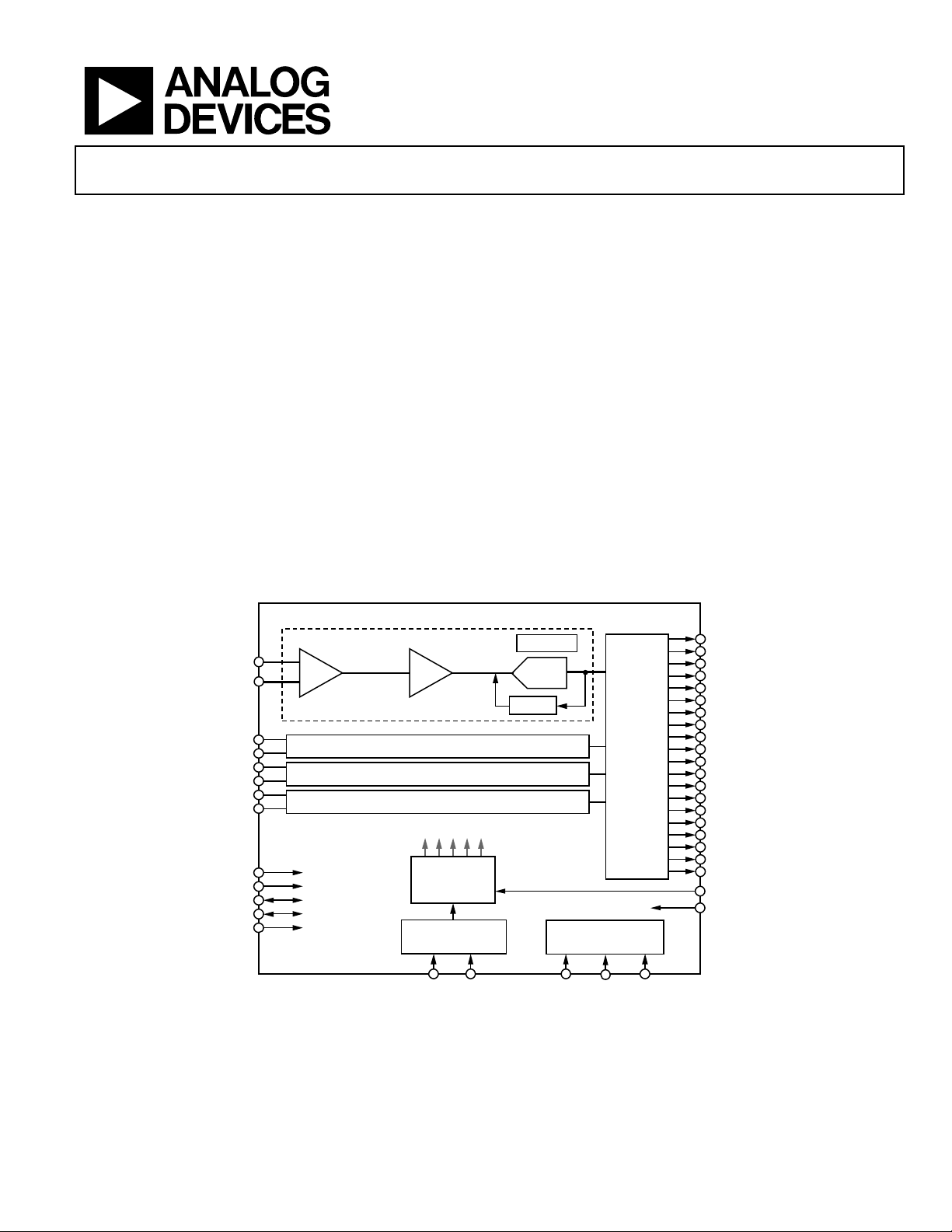
FUNCTIONAL BLOCK DIAGRAM
ADDI7004
INP_A
INM_A
INP_B
INM_B
INP_C
INM_C
INP_D
INM_D
SHP
SHD
CLPOB
PBLK
DCR
CDS/
SHA
–3dB, 0dB, +3d B, +6dB
NOTES
1. THE CIRCUI T RY FOR AFE1 TO AFE4 IS IDENTICAL .
AFE1
VGA
6dB ~ 42dB
AFE2
AFE3
AFE4
INTERNAL CL OCKS
Precision
Timing
CORE
SYNC
GENERATOR
VDHD
Figure 1.
For more information on the ADDI7004, email Analog Devices, Inc., at afe.ccd@analog.com.
VREF
ADC
CLAMP
INTERNAL
REGISTERS
SL
SDATA
REDUCED
RANGE
LVDS
INTERFACE
SCK
DOUT0P
DOUT0N
DOUT1P
DOUT1N
DOUT2P
DOUT2N
DOUT3P
DOUT3N
TCLK0P
TCLK0N
TCLK1P
TCLK1N
DOUT4P
DOUT4N
DOUT5P
DOUT5N
DOUT6P
DOUT6N
DOUT7P
DOUT7N
CLI
RSTB
07799-001
Rev. SpC
Information furnished by Analog Devices is believed to be accurate and reliable. However, no
responsibility is assumed by Anal og Devices for its use, nor for any infringements of patents or ot her
rights of third parties that may result from its use. Specifications subject to change without notice. No
license is granted by implication or otherwise under any patent or patent rights of Analog Devices.
Trademarks and registered trademarks are the property of their respective owners.
One Technology Way, P.O. Box 9106, Norwood, MA 02062-9106, U.S.A.
Tel: 781.329.4700 www.analog.com
Fax: 781.461.3113 ©2008–2011 Analog Devices, Inc. All rights reserved.

ADDI7004
NOTES
©2008–2011 Analog Devices, Inc. All rights reserved. Trademarks and
registered trademarks are the property of their respective owners.
D07799F-0-1/11(SpC)
Rev. SpC | Page 2 of 2
 Loading...