Analog Devices ADDAC87D-CBI-V, ADDAC87-CBII883, ADDAC87-CBI-V, ADDAC87-CBI-I, ADDAC85MILCBIV8 Datasheet
...
REV. B
Information furnished by Analog Devices is believed to be accurate and
reliable. However, no responsibility is assumed by Analog Devices for its
use, nor for any infringements of patents or other rights of third parties that
may result from its use. No license is granted by implication or otherwise
under any patent or patent rights of Analog Devices.
a
ADDAC80/ADDAC85/ADDAC87
One Technology Way, P.O. Box 9106, Norwood, MA 02062-9106, U.S.A.
Tel: 781/329-4700 www.analog.com
Fax: 781/326-8703 © Analog Devices, Inc., 2002
Complete Low Cost
12-Bit D/A Converters
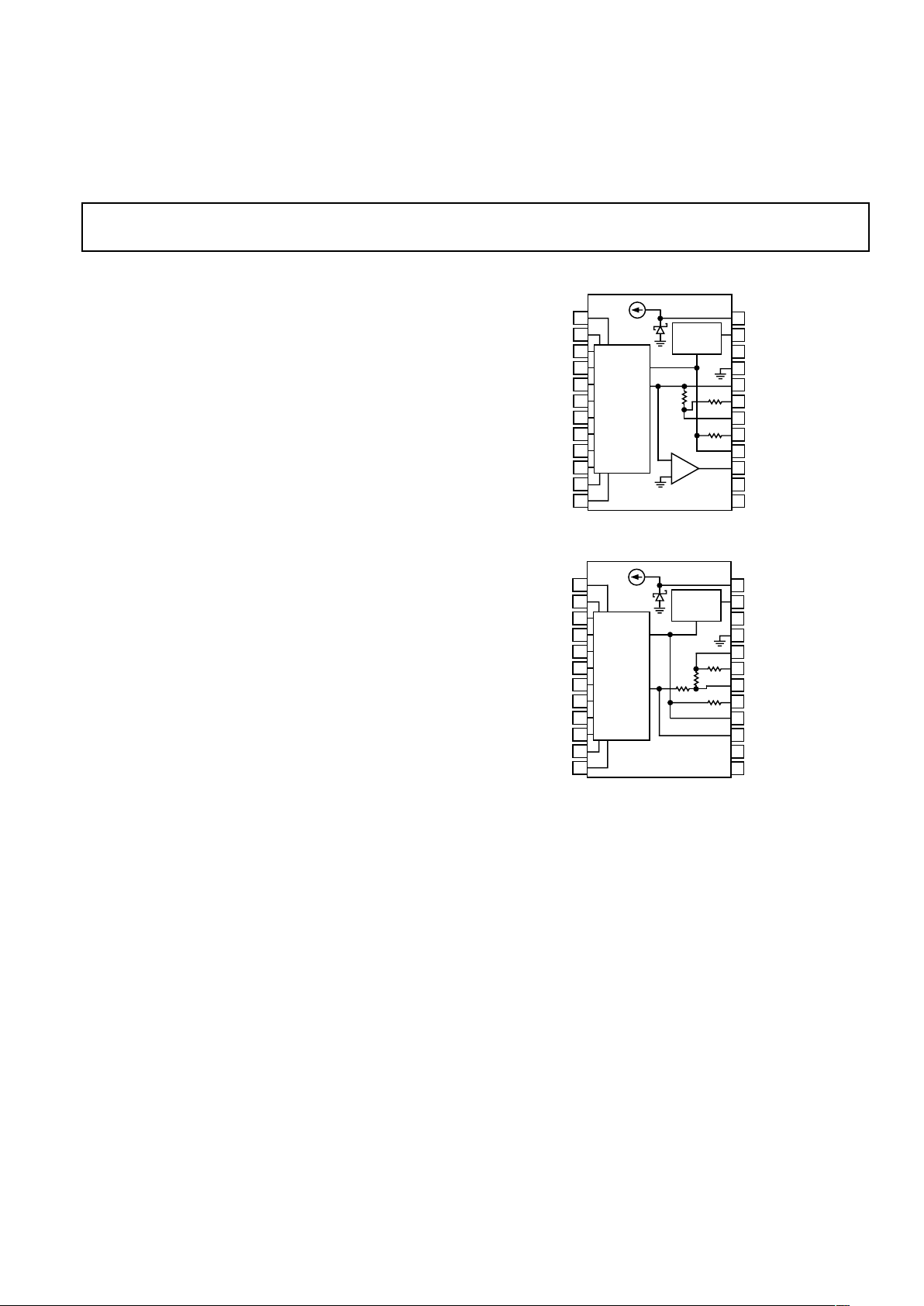
FUNCTIONAL BLOCK DIAGRAM
*NC = CBI VERSIONS
5V – CCD VERSIONS
(MSB) BIT 1
BIT 2
BIT 3
BIT 4
BIT 5
BIT 6
BIT 7
BIT 8
BIT 9
BIT 10
BIT 11
(LSB) BIT 12
V
REF
OUT
GAIN ADJUST
+V
S
COMMON
SUMMING JUNCTION
20V RANGE
10V RANGE
BIPOLAR OFFSET
REF INPUT
V
OUT
–V
S
NC/+VL*
12-BIT
RESISTOR
LADDER
NETWORK
AND
CURRENT
SWITCHES
REF
CONTROL
CIRCUIT
1
2
3
4
5
6
7
8
9
10
11
12
24
23
22
21
20
19
18
17
16
15
14
13
6.3k
5k
5k
ADDAC80
+
–
*NC = CBI VERSIONS
5V – CCD VERSIONS
(MSB) BIT 1
BIT 2
BIT 3
BIT 4
BIT 5
BIT 6
BIT 7
BIT 8
BIT 9
BIT 10
BIT 11
(LSB) BIT 12
V
REF
OUT
GAIN ADJUST
+V
S
COMMON
SCALING NETWORK
SCALING NETWORK
SCALING NETWORK
BIPOLAR OFFSET
REF INPUT
I
OUT
–V
S
NC/+VL*
12-BIT
RESISTOR
LADDER
NETWORK
AND
CURRENT
SWITCHES
REF
CONTROL
CIRCUIT
1
2
3
4
5
6
7
8
9
10
11
12
24
23
22
21
20
19
18
17
16
15
14
13
6.3k
2k
5k
5k
FEATURES
Single Chip Construction
On-Board Output Amplifier
Low Power Dissipation: 300 mW
Monotonicity Guaranteed over Temperature
Guaranteed for Operation with 12 V Supplies
Improved Replacement for Standard DAC80, DAC800
Hl-5680
High Stability, High Current Output
Buried Zener Reference
Laser Trimmed to High Accuracy
1/2 LSB Max Nonlinearity
Low Cost Plastic Packaging
PRODUCT DESCRIPTION
The ADDAC80 Series is a family of low cost 12-bit digital-toanalog converters with both a high stability voltage reference
and output amplifier combined on a single monolithic chip.
The ADDAC80 Series is recommended for all low cost 12-bit D/A
converter applications where reliability and cost are of paramount
importance.
Advanced circuit design and precision processing techniques
result in significant performance advantages over conventional
DAC80 devices. Innovative circuit design reduces the total
power consumption to 300 mW, which not only improves reliability, but also improves long term stability.
The ADDAC80 incorporates a fully differential, nonsaturating
precision current switching cell structure which provides greatly
increased immunity to supply voltage variation. This same structure
also reduces nonlinearities due to thermal transients as the
various bits are switched; nearly all critical components operate
at constant power dissipation. High stability, SiCr thin film
resistors are trimmed with a fine resolution laser, resulting in
lower differential nonlinearity errors. A low noise, high stability,
subsurface Zener diode is used to produce a reference voltage
with excellent long term stability, high external current capability and temperature drift characteristics which challenge the
best discrete Zener references.
The ADDAC80 Series is available in three performance grades
and three package types. The ADDAC80 is specified for use
over the 0°C to 70°C temperature range and is available in
both plastic and ceramic DIP packages. The ADDAC85 and
ADDAC87 are av
ailable in hermetically sealed ceramic packages
and are specified
for the –25°C to +85°C and –55°C to +125°C
temperature ranges.
PRODUCT HIGHLIGHTS
1. The ADDAC80 series of D/A converters directly replaces all
other devices of this type with significant increases in performance.
2. Single chip construction and low power consumption provides the optimum choice for applications where low cost
and high reliability are major considerations.
3. The high speed output amplifier has been designed to settle
within 1/2 LSB for a 10 V full scale transition in 2.0 µs, when
properly compensated.
4.
The precision buried Zener reference can supply up to 2.5 mA
for use elsewhere in the application.
5. The low TC binary ladder guarantees that all units are monotonic over the specified temperature range.
6. System performance upgrading is possible without redesign.

REV. B
–2–
ADDAC80/ADDAC85/ADDAC87–SPECIFICATIONS
ADDAC80 ADDAC85 ADDAC87
Model Min Typ Max Min Typ Max Min Typ Max Unit
TECHNOLOGY Monolithic Monolithic Monolithic
DIGITAL INPUT
Binary–CBI 12 12 12 Bits
BCD–CCD Digits
Logic Levels (TTL Compatible)
V
IH
(Logic “1”) 2.0 5.5 2.0 5.5 2.0 5.5 V
VIL (Logic “0”) 0 0.8 0 0.8 0 0.8 V
IIH (V
IH
= 5.5 V) 250 250 250 µA
IIL (V
IL
= 0.8 V) 100 100 100 µA
TRANSFER CHARACTERISTICS
ACCURACY
Linearity Error @ 25°C
CBI ±1/2 ±1/2 ± 1/2 LSB
1
CCD LSB
TA @ T
MIN
to T
MAX
±1/4±1/2 ±1/4±1/2 ±1/2±3/4 LSB
Differential Linearity Error @ 25°C
CBI
±
3/4
±
3/4
±
3/4 LSB
CCD LSB
TA @ T
MIN
to T
MAX
±
3/4
±
1
±
1 LSB
Gain Error
2
±0.1±0.3 ± 0.1±0.2 ± 0.1±0.2 %FSR
3
Offset Error
2
±0.05±0.15 ±0.05±0.1 ± 0.05±0.1 %FSR
3
Temperature Range for Guaranteed
Monotonicity 0 +70 –25 +85 –55 +125 °C
DRIFT (T
MIN
to T
MAX
)
Total Bipolar Drift, max (includes gain,
offset, and linearity drifts) ±20 ±20 ±30 ppm of FSR/°C
Total Error (T
MIN
to T
MAX
)
4
Unipolar ±0.08 ±0.15 ±0.12 ±0.2 ± 0.18 ± 0.3 % of FSR
Bipolar ±0.06 ±0.10 ±0.08 ±0.12 ±0.14 ±0.24 % of FSR
Gain Including Internal Reference ±15
±
30
±
20
±
20 ppm of FSR/°C
Gain Excluding Internal Reference ±4 ±7 ± 10 ± 10 ppm of FSR/°C
Unipolar Offset ±1
±
3
±
3
±
3 ppm of FSR/°C
Bipolar Offset ±5
±
10
±
10
±
10 ppm of FSR/°C
CONVERSION SPEED
Voltage Model (V)
5
Settling Time to ±0.01% of FSR for
FSR Change (2 kΩ储500 pF load)
with 10 kΩ Feedback 3 4 3 4 3 4 µs
with 5 kΩ Feedback 2 3 2 3 2 3 µs
For LSB Change 1 1 1 µs
Slew Rate 10 10 10 V/µs
ANALOG OUTPUT
Voltage Models
Ranges–CBI
±2.5, ±5, ±2.5, ±5,
±2.5, ±5,
V
±10, +5, ±10, +5, ±10, +5, V
10 10 10 V
–CCD V
Output Current ±5 ±5 ±5mA
Output Impedance (dc) 0.05 0.05 0.05 Ω
Short Circuit Current 40 40 40 mA
Internal Reference Voltage (VR) 6.23 6.3 6.37 6.23 6.3 6.37 6.23 6.3 6.37 V
Output Impedance 1.5 1.5 1.5 Ω
Max External Current
6
2.5 2.5 2.5 mA
Tempco of Drift ±10 ±20 ±10 ±20 ±10 ppm of VR/°C
POWER SUPPLY SENSITIVITY
±15 V ± 10%, 5 V supply when applicable 0.002 0.002 0.002 % of FSR/%V
S
±12 V ± 5% 0.002 0.002 0.002 % of FSR/%V
S
POWER SUPPLY REQUIREMENTS
Rated Voltages ±15 ±15 ±15 V
Range
Analog Supplies ±11.4
7
±16.5 ±11.4
7
±16.5 ±11.4
7
±16.5 V
Logic Supplies V
Supply Drain
+12 V, +15 V 5 10 5 10 5 10 mA
–12 V, –15 V 14 20 14 20 14 20 mA
(TA = 25C, rated power supplies
unless
otherwise noted.)

REV. B
–3–
ADDAC80/ADDAC85/ADDAC87
ADDAC80 ADDAC85 ADDAC87
Model Min Typ Max Min Typ Max Min Typ Max Unit
TEMPERATURE RANGE
Specifications 0 +70 –25 +85 –55 +125 °C
Operating –25 +85 –55 +125 –55 +125 °C
Storage –25 +125 –65 +150 –65 +150 °C
NOTES
1
Least Significant Bit.
2
Adjustable to zero with external trim potentiometer.
3
FSR means “Full Scale Range” and is 20 V for the ± 10 V range and 10 V for the ±5 V range.
4
Gain and offset errors adjusted to zero at 25°C.
5
CF = 0, see Figure 3a.
6
Maximum with no degradation of specification, must be a constant load.
7
A minimum of ±12.3 V is required for a ± 10 V full scale output and ±11.4 V is required for all other voltage ranges.
Specifications shown in boldface are tested on all production units at final electrical test. Results from those tests are used to calculate outgoing quality levels. All min
and max specifications are guaranteed, although only those shown in boldface are tested on all production units.
Specifications subject to change without notice.
ADDAC80 ADDAC85 ADDAC87
Model Min Typ Max Min Typ Max Min Typ Max Unit
TECHNOLOGY Hybrid Hybrid Hybrid
DIGITAL INPUT
Binary–CBI 12 12 12 Bits
BCD–CCD 3 3 3 Digits
Logic Levels (TTL Compatible)
VIH (Logic “1”) 2.0 5.5 2.0 5.5 2.0 5.5 V
VIL (Logic “0”) 0 0.8 0 0.8 0 0.8 V
IIH (V
IH
= 5.5 V) 250 250 250 µA
IIL (V
IL
= 0.8 V) –100 –100 –100 µA
TRANSFER CHARACTERISTICS
ACCURACY
Linearity Error @ 25°C
CBI ±1/4 ±1/2 ±1/2 ± 1/2 LSB
1
CCD ±1/8 ±1/4 ±1/4 ± 1/4 LSB
TA @ T
MIN
to T
MAX
±1/4 ±1/2 ± 1/4 ± 1/2 ±1/2 ±1/2 LSB
Differential Linearity Error @ 25°C
CBI ±1/2 ±3/4 ± 1/2 ± 1/2 LSB
CCD ±1/4 ±1/2 ± 1/2 ± 1/2 LSB
TA @ T
MIN
to T
MAX
±1 ± 1 ± 1 LSB
Gain Error
2
±0.1 ±0.3 ± 0.1 ± 0.1 %FSR
3
Offset Error
2
±0.05 ±0.15 ±0.05 ±0.05 %FSR
3
Temperature Range for Guaranteed
Monotonicity 0 +70 0 +70 –25 +85 °C
DRIFT (T
MIN
to T
MAX
)
Total Bipolar Drift, max (includes gain,
offset, and linearity drifts) ±20 ppm of FSR/°C
Total Error (T
MIN
to T
MAX
)
4
Unipolar ±0.08 ±0.15 % of FSR
Bipolar ±0.06 ±0.10 % of FSR
Gain
Including Internal Reference ±15 ±30 ±20 ±20 ppm of FSR/°C
Excluding Internal Reference ± 5 ± 7 ± 10 ± 10 ppm of FSR/°C
Unipolar Offset ±1 ±3 ±1 ± 1 ppm of FSR/°C
Bipolar Offset ±5 ±10 ±10 ±10 ppm of FSR/°C
CONVERSION SPEED
Voltage Model (V)
5
Settling Time to ±0.01% of FSR for
FSR Change (2 kΩ储500 pF load)
with 10 kΩ Feedback 5 5 5 µs
with 5 kΩ Feedback 3 3 3 µs
For LSB Change 1.5 1.5 1.5 µs
Slew Rate 10 15 20 20 V/µs
Current Model (I)
Settling time to ±0.01% of FSR for
FSR Change
10 Ω to 100 Ω Load 300 300 300 ns
for 1 kΩ 111µs

REV. B
–4–
ADDAC80/ADDAC85/ADDAC87–SPECIFICATIONS
ADDAC80 ADDAC85 ADDAC87
Model Min Typ Max Min Typ Max Min Typ Max Unit
ANALOG OUTPUT
Voltage Models
Ranges–CBI ±2.5, ±5, ±2.5, ±5, ±2.5, ±5,
±10, +5, ±10, +5, ±10, +5,
+10 +10 +10 V
Ranges–CCD ±10 +10 +10 V
Output Current ±5 ±5 ±5mA
Output Impedance (dc) 0.05 0.05 0.05 Ω
Short Circuit Duration
Indefinite to Common Indefinite to Common Indefinite to Common
Current Models
Ranges–Unipolar –2.0 –2.0 –2.0 mA
Ranges–Bipolar ±1.0 ±1.0 ±1.0 mA
Output Impedance
Bipolar 3.2 3.2 3.2 kΩ
Unipolar 6.6 6.6 6.6 kΩ
Compliance –1.5, +10 –2.5, +10 –2.5, +10 V
Internal Reference Voltage (VR) 6.17 6.3 6.43 6.17 6.3 6.43 6.17 6.3 6.43 V
Output Impedance 1.5 1.5 1.5 Ω
Max External Current
6
2.5 2.5 2.5 mA
Tempco of Drift ±10 ±20 ±10 ±20 ±10 ±20 ppm of VR/°C
POWER SUPPLY SENSITIVITY
±15 V ± 10%, 5 V Supply When Applicable
±0.002 ±0.002 ± 0.002 % of FSR/%V
S
POWER SUPPLY REQUIREMENTS
Rated Voltages ±15, +5 ±15, +5 ±15, +5 V
Range
Analog Supplies ±14 ±16 ± 14.5 ±15.5 ±14.5 ± 15.5 V
Logic Supplies 4.5 16 4.5 15.5 4.5 15.5 V
Supply Drain
7
+15 V 10 20 15 20 15 20 mA
–15 V 20 35 25 30 25 30 mA
+5 V
8
82015201520mA
TEMPERATURE RANGE
Specifications 0 +70 0 +70 –25 +85 °C
Operating –25 +85 –25 +85 –55 +125 °C
Storage –55 +130 –65 +150 –65 +150 °C
NOTES
1
Least Significant Bit.
2
Adjustable to zero with external trim potentiometer.
3
FSR means “Full Scale Range” and is 20 V for the ± 10 V range and 10 V for the ±5 V range.
4
Gain and offset errors adjusted to zero at 25°C.
5
CF = 0, see Figure 3a.
6
Maximum with no degradation of specification, must be a constant load.
7
Including 5 mA load.
8
5 V supply required only for CCD versions.
Specifications subject to change without notice.
(continued)

REV. B
–5–
ADDAC80/ADDAC85/ADDAC87
ADDAC85LD ADDAC85MIL ADDAC87
Model Min Typ Max Min Typ Max Min Typ Max Unit
TECHNOLOGY Hybrid Hybrid Hybrid
DIGITAL INPUT
Binary–CBI 12 12 12 Bits
BCD–CCD Digits
Logic Levels (TTL Compatible)
VIH (Logic “1”) 2.0 5.5 2.0 5.5 2.0 5.5 V
VIL (Logic “0”) 0 0.8 0 0.8 0 0.8 V
IIH (V
IH
= 5.5 V) 250 250 250 µA
IIL (V
IL
= 0.8 V) –100 –100 –100 µA
TRANSFER CHARACTERISTICS
ACCURACY
Linearity Error @ 25°C
CBI ±1/2 ±1/2 ± 1/4 ± 1/2 LSB
1
CCD LSB
TA @ T
MIN
to T
MAX
±1/2 ±3/4 ± 3/4 LSB
Differential Linearity Error @ 25°C
CBI ±1/2 ±1/2 ± 1/2 LSB
CCD LSB
TA @ T
MIN
to T
MAX
±1 ± 1 ± 1 LSB
Gain Error
2
±0.1 ±0.1 ±0.1 ±0.2 %FSR
3
Offset Error
2
±0.05 ±0.05 ±0.05 ±0.1 %FSR
3
Temperature Range for Guaranteed
Monotonicity –25 +85 –55 +125 –55 +125 °C
DRIFT (T
MIN
to T
MAX
)
Total Bipolar Drift, max (includes gain,
offset, and linearity drifts) ±15 ±30 ppm of FSR/°C
Total Error (T
MIN
to T
MAX
)
4
Unipolar ±0.13 ±0.30 % of FSR
Bipolar ±0.12 ±0.24 % of FSR
Gain
Including Internal Reference ±10 ±20 ±10 ±25 ppm of FSR/°C
Excluding Internal Reference ±5 ±10 ppm of FSR/°C
Unipolar Offset ±1 ± 2 ± 1 ± 3 ppm of FSR/°C
Bipolar Offset ±5 ± 10 ± 5 ± 10 ppm of FSR/°C
CONVERSION SPEED
Voltage Model (V)
5
Settling Time to ±0.01% of FSR
for FSR change (2 kΩ储500 pF load)
with 10 kΩ Feedback 5 5 5 µs
with 5 kΩ Feedback 3 3 3 µs
For LSB Change 1.5 1.5 1.5 µs
Slew Rate 20 20 20 V/µs
Current Model (I)
Settling Time to ±0.01% of FSR
for FSR Change
10 Ω to 100 Ω Load 300 300 300 ns
for 1 kΩ 111µs
ANALOG OUTPUT
Voltage Models
Ranges–CBI ±2.5, ±5, ±2.5, ±5, ±2.5, ±5,
±10, +5, ±10, +5, ±10, +5,
+10 +10 +10 V
Ranges–CCD V
Output Current ±5 ±5 ±5mA
Output Impedance (dc)
0.05 0.05 0.05 Ω
Short Circuit Duration Indefinite to Common Indefinite to Common Indefinite to Common
Current Models
Ranges–Unipolar –2.0 –2.0 –2.0 mA
Ranges–Bipolar ±1.0 ± 1.0 ± 1.0 mA
Output Impedance
Bipolar 3.2 3.2 2.5 3.2 4.1 kΩ
Unipolar 6.6 6.6 5.0 6.6 8.2 kΩ
Compliance –2.5, +10 –2.5, +10 –1.5, +10 V
Internal Reference Voltage (VR) 6.17 6.3 6.43 6.17 6.3 6.43 6.17 6.3 6.43 V
Output Impedance 1.5 1.5 1.5 Ω
Max External Current
6
2.5 2.5 2.5 mA
Tempco of Drift ±10 ±20 ±10 ±20 ±5 ±10 ppm of VR/°C
POWER SUPPLY SENSITIVITY
±15 V ± 10%, 5 V supply when applicable
±0.002 ±0.002 ± 0.002 ±0.003 % of
FSR/%V
S
 Loading...