

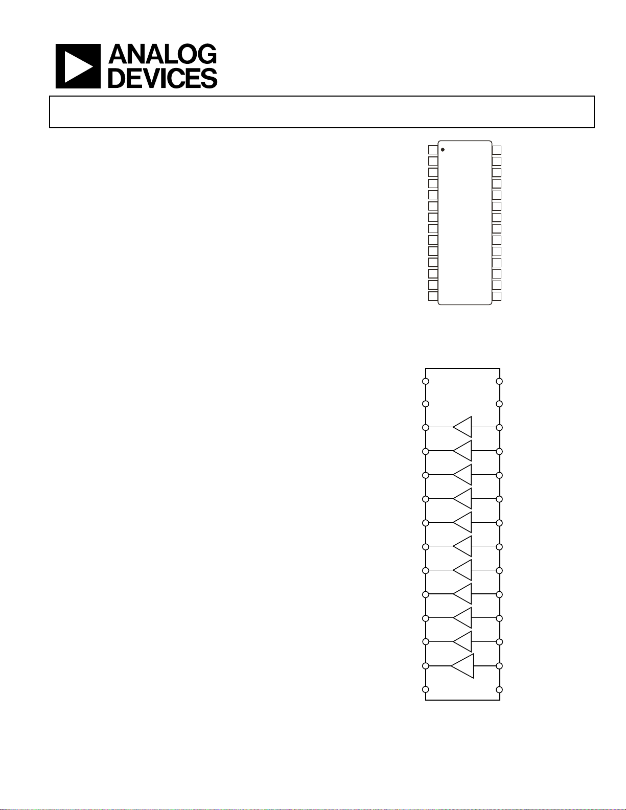
10-Channel Gamma Buffer
FEATURES
Single-supply operation: 4.5 V to 18 V
Upper/lower buffers swing to V
Gamma continuous output current: >10 mA
peak output current: 250 mA
V
COM
Offset voltage: 12 mV
Slew rate: 8 V/µs
Unity gain stable with large capacitive loads
Supply current: 700 µA per amplifier
Compact 28-lead TSSOP
Pb-free package
Drop-in replacement for BUF11702
APPLICATIONS
TFT LCD monitor panels
TFT LCD notebook panels
GENERAL DESCRIPTION
The ADD8710 is a low cost, 10-channel gamma buffer with a
V
driver that operates from a single supply. The part is
COM
designed for high resolution TFT LCD panels and is built on an
advanced, high voltage CBCMOS process.
The gamma buffers have a high slew rate, minimum 10 mA
output current, and a high capacitive load drive capability. The
buffer is capable of delivering 250 mA of peak current and
V
COM
can also drive large capacitive loads. The ADD8710 offers wide
supply range and offset voltages below 12 mV.
The ADD8710 is specified over the −40°C to +85°C
temperature range and is available in a Pb-free, 28-lead
TSSOP package.
/GND
S
with V
COM
ADD8710
1
V
S
2
NC
3
OUT1
4
OUT2
5
OUT3
6
OUT4
7
OUT5
OUT6
OUT7
OUT8
OUT9
OUT10
OUTCOM
GND
NC = NO CONNECT
8
9
10
11
12
13
14
ADD8710
Figure 1. 28-Lead TSSOP (RU Suffix)
FUNCTIONAL BLOCK DIAGRAM
V
NC
OUT1
OUT2
OUT3
OUT4
OUT5
OUT6
OUT7
ADD8710
S
1
2
3
4
5
6
7
28
V
S
27
NC
26
IN1
25
IN2
24
IN3
23
IN4
22
IN5
21
IN6
20
IN7
19
IN8
18
IN9
17
IN10
16
INCOM
15
GND
04889-001
V
S
NC
IN1
IN2
IN3
IN4
IN5
IN6
IN7
Driver
Rev. A
Information furnished by Analog Devices is believed to be accurate and reliable.
However, no responsibility is assumed by Analog Devices for its use, nor for any
infringements of patents or other rights of third parties that may result from its use.
Specifications subject to change without notice. No license is granted by implication
or otherwise under any patent or patent rights of Analog Devices. Trademarks and
registered trademarks are the property of their respective owners.
OUT8
OUT9
OUT10
OUTCOM
GND
One Technology Way, P.O. Box 9106, Norwood, MA 02062-9106, U.S.A.
8
9
10
V
COM
Figure 2.
IN8
IN9
IN10
INCOM
GND
Tel: 781.329.4700 www.analog.com
Fax: 781.326.8703 © 2005 Analog Devices, Inc. All rights reserved.
04889-002

ADD8710
TABLE OF CONTENTS
Electrical Characteristics ................................................................. 3
Typical Performance Characteristics..............................................5
Absolute Maximum Ratings............................................................ 4
ESD Caution.................................................................................. 4
REVISION HISTORY
13/05—Rev. 0 to Rev. A
Change to Features........................................................................... 1
Changes to Specifications................................................................ 3
Change to Absolute Maximum Ratings......................................... 4
6/04—Revision 0: Initial Version
Outline Dimensions....................................................................... 10
Ordering Guide .......................................................................... 10
Rev. A | Page 2 of 12

ADD8710
ELECTRICAL CHARACTERISTICS
VS = 16 V, VCM = VS/2, TA @ 25°C, unless otherwise noted.
Table 1.
Parameter Symbol Condition Min Typ Max Unit
INPUT CHARACTERISTICS Applies to all channels
Offset Voltage VOS 4 12 mV
Offset Voltage Drift ∆VOS/∆T −40°C ≤ TA ≤ +85°C 5 µV/°C
Input Bias Current IB 0.5 1.1 µA
−40°C ≤ TA ≤ +85°C 1.5 µA
Input Impedance ZIN 400 kΩ
Input Capacitance CIN 1 pF
BUFFER CHARACTERISTICS
Common-Mode Input Range V
Buffers 1 to 5 1.25 VS V
Buffers 6 to 10 0 VS − 1.25 V
Output Voltage High (V1) VOH V
V
−40°C ≤ TA ≤ +85°C 9.7 V
Output Voltage High (V2 to V5) VOH V
−40°C ≤ TA ≤ +85°C 8.4 V
Output Voltage High (V6 to V10) VOH V
−40°C ≤ TA ≤ +85°C 7.9 V
Output Voltage Low (V1 to V5) VOL V
−40°C ≤ TA ≤ +85°C 2.10 V
Output Voltage Low (V6 to V9) VOL V
−40°C ≤ TA ≤ +85°C 1.60 V
Output Voltage Low (V10) VOL V
V
−40°C ≤ TA ≤ +85°C 0.3 V
Continuous Output Current I
Peak Output Current IPK V
V
CHARACTERISTICS
COM
Common-Mode Input Range V
Output Voltage High VOH V
−40°C ≤ TA ≤ +85°C 7.9
Output Voltage Low VOL V
−40°C ≤ TA ≤ +85°C 2.10
Continuous Output Current I
Peak Output Current IPK V
SUPPLY CHARACTERISTICS
Supply Voltage VS 4.5 18 V
Power Supply Rejection Ratio PSRR VS = 4.5 V to 16.5 V, −40°C ≤ TA ≤ +85°C 70 90 dB
Total Supply Current ISY V
−40°C ≤ TA ≤ +85°C 11.5 mA
DYNAMIC PERFORMANCE
Slew Rate SR RL = 2 kΩ, CL = 200 pF 4 8 V/µs
Bandwidth BW −3 dB, RL = 10 kΩ, CL = 200 pF 5 MHz
Settling Time to 0.1% (Buffers) tS 1 V step, RL = 10 kΩ, CL = 200 pF 1.1 µs
Settling Time to 0.1% (V
) tS 1 V step, RL = 10 kΩ, CL = 200 pF 0.7 µs
COM
Phase Margin Øo RL = 10 kΩ, CL = 200 pF 45 Degree
Channel Separation 75 dB
CMM
= 16 V, VI = 16 V, IL = 10 mA 15.82 15.9 V
S
= 10 V, VI = 9.8 V, IL = 10 mA 9.75 9.8 V
S
= 10 V, VI = 8.5 V, IL = 10 mA 8.45 8.5 V
S
= 10 V, VI = 8 V, IL = 10 mA 7.95 8 V
S
= 10 V, VI = 2 V, IL = 10 mA 2 2.05 V
S
= 10 V, VI = 1.5 V, IL = 10 mA 1.5 1.55 V
S
= 16 V, VI = 0 V, IL = 10 mA 0.1 0.175 V
S
= 10 V, VI = 0.2 V, IL = 10 mA 0.2 0.25 V
S
10 mA
OUT
= 16 V 100 mA
S
0 VS − 1.25 V
CMM
= 10 V, VI = 8 V, IL = 30 mA 7.95 8
S
= 10 V, VI = 2 V, IL = 30 mA 2 2.05
S
35 mA
OUT
= 16 V 250 mA
S
= VS/2, no load 7.7 10 mA
O
Rev. A | Page 3 of 12
ADD8710
ABSOLUTE MAXIMUM RATINGS
Table 2.
Parameter Rating
Supply Voltage (VS) 18.5 V
Input Voltage −0.5 V to VS + 0.5 V
Storage Temperature Range −65°C to +150°C
Operating Temperature Range −40°C to +85°C
Junction Temperature Range −65°C to +150°C
Lead Temperature Range 300°C
ESD Tolerance (HBM) ±2500 V
ESD Tolerance (MM) ±200 V
Stresses above those listed under Absolute Maximum Ratings
may cause permanent damage to the device. This is a stress
rating only; functional operation of the device at these or any
other conditions above those indicated in the operational
sections of this specification is not implied. Exposure to
absolute maximum rating conditions for extended periods may
affect device reliability.
Table 3. Package Characteristics
Package Type θ
28-Lead TSSOP (RU) 67.7 °C/W
1
θJA is specified for worst-case conditions, i.e., θJA is specified for devices
soldered onto a circuit board for surface-mount packages.
1
Unit
JA
ESD CAUTION
ESD (electrostatic discharge) sensitive device. Electrostatic charges as high as 4000 V readily accumulate on
the human body and test equipment and can discharge without detection. Although this product features
proprietary ESD protection circuitry, permanent damage may occur on devices subjected to high energy
electrostatic discharges. Therefore, proper ESD precautions are recommended to avoid performance
degradation or loss of functionality.
Rev. A | Page 4 of 12

ADD8710
TYPICAL PERFORMANCE CHARACTERISTICS
800
700
600
500
400
300
NUMBER OF UNITS
200
100
T = 25°C
= 4.5V TO 16V
V
DD
0.7
0.6
0.5
0.4
0.3
0.2
SUPPLY CURRENT/BUFFER (mA)
0.1
0
–8 8–7 7–6 6–5 5–4 4–3 3–2 2–1 10
V
(mV)
OS
Figure 3. Input Offset Voltage
300
250
200
150
100
NUMBER OF UNITS
50
0
6
9
3
121518
3
3
39
TCVOS (µV/°C)
Figure 4. Input Offset Voltage Drift Distribution
0
04889-003
0 2 4 6 8 10 12 14 16 18
SUPPLY VOLTAGE (V)
04889-006
Figure 6. Supply Current/Buffer vs. Supply Voltage
1.0
0.9
0.8
0.7
0.6
0.5
0.4
0.3
0.2
SUPPLY CURRENT/BUFFER (mA)
0.1
4
42
603657
485145
5
78
752172246927663063
04889-004
0
TEMPERATURE (°C)
120–40 –20 0 20 40 60 80 100
04889-007
Figure 7. Supply Current/Buffer vs. Temperature
5
4
3
2
1
0
–1
–2
INPUT OFFSET VOLTAGE (mV)
–3
–4
–40
–20
020
40
TEMPERATURE (°C)
80
60
Figure 5. Input Offset Voltage vs. Temperature
V7
V1
V8
V2
V9
V3
V10
V4
V
V5
COM
V6
120
100
04889-005
600
400
200
INPUT BIAS CURRENT (nA)
–200
–400
0
–40
–20
020
TEMPERATURE (°C)
60
40
Figure 8. Input Bias Current vs. Temperature
V1
V7
V2
V8
V3
V9
V4
V10
V5
V
COM
V6
100
120
04889-008
80
Rev. A | Page 5 of 12

ADD8710
125
105
95
75
V
55
35
(dB)
15
–5
–25
–45
–65
Figure 9. Power Supply Rejection Ratio vs. Frequency
COM
V1–V10
100k10k1k100 1M 10M
FREQUENCY (Hz)
04889-009
1.0
VIN = 0V
0.9
0.8
0.7
0.6
0.5
0.4
0.3
OUTPUT VOLTAGE (V)
0.2
0.1
0
Figure 12. Channel V
101 100
LOAD CURRENT (mA)
Output Voltage Low vs. I Load
COM
04889-012
2.5
VIN = 0V
2.0
1.5
1.0
OUTPUT VOLTAGE (V)
0.5
0
101 100
LOAD CURRENT (mA)
Figure 10. Channels 1 to 5 Output Voltage Low vs. I Load
1.4
VIN = 0V
1.2
1.0
0.8
04889-010
16.2
16.0
15.8
15.6
15.4
15.2
15.0
14.8
OUTPUT VOLTAGE (V)
14.6
14.4
14.2
Figure 13. Channel 1 Output Voltage High vs. I Load
10.00
9.99
9.98
9.97
101 100
LOAD CURRENT (mA)
VIN = 16V
VIN = 10V
04889-013
0.6
OUTPUT VOLTAGE (V)
0.4
0.2
0
101 100
LOAD CURRENT (mA)
Figure 11. Channels 6 to 10 Output Voltage Low vs. I Load
04889-011
Rev. A | Page 6 of 12
9.96
OUTPUT VOLTAGE (V)
9.95
9.94
9.93
101 100
LOAD CURRENT (mA)
Figure 14. Channels 2 to 5 Output Voltage High vs. I Load
04889-014

ADD8710
11
9
7
5
RL = 2kΩ
C
LOAD
= 100pF
3
OUTPUT VOLTAGE (V)
1
VIN = 10V
–1
101 100
LOAD CURRENT (mA)
Figure 15. Channels 6 to 10 Output Voltage High vs. I Load
10.00
9.99
9.98
9.97
9.96
9.95
9.94
9.93
OUTPUT VOLTAGE (V)
9.92
9.91
9.90
Figure 16. Channel V
101 100
LOAD CURRENT (mA)
Output Voltage High vs. I Load
COM
VIN = 10V
04889-015
04889-016
VOLTAGE (4V/DIV)
TIME (2µs/DIV)
Figure 18. Large-Signal Transient Response
20
10
0
–10
–20
–30
(dB)
–40
–50
–60
–70
–80
100k 1M 10M
1040pF
510pF
FREQUENCY (Hz)
140pF
90pF
40pF
Figure 19. Channels 1 to 5 Frequency Response vs. Capacitive Loading
04889-018
04889-019
RL = 2kΩ
C
= 100pF
LOAD
VOLTAGE (50mV/DIV)
TIME (2µs/DIV)
04889-017
Figure 17. Small-Signal Transient Response
20
10
0
–10
–20
–30
(dB)
–40
–50
–60
–70
–80
100k 1M 10M
1040pF
510pF
FREQUENCY (Hz)
140pF
90pF
40pF
Figure 20. Channels 6 to 10 Frequency Response vs. Capacitive Loading
04889-020
Rev. A | Page 7 of 12

ADD8710
20
10
0
–10
–20
–30
(dB)
–40
–50
–60
–70
–80
100k 1M 10M
Figure 21. Channel V
Frequency Response vs. Capacitive Loading
COM
1040pF
FREQUENCY (Hz)
510pF
140pF
90pF
40pF
04889-021
10
5
0
–5
–10
–15
(dB)
–20
–25
–30
–35
–40
100k
Figure 24. Channel V
10kΩ
150Ω
1M 10M 100M
FREQUENCY (Hz)
Frequency Response vs. Resistive Loading
COM
2kΩ
1kΩ
560Ω
04889-024
10
(dB)
–10
–15
–20
–25
–30
–35
–40
–5
5
0
100k
10kΩ
1M 10M 100M
FREQUENCY (Hz)
2kΩ
1kΩ
560Ω
150Ω
Figure 22. Channels 1 to 5 Frequency Response vs. Resistive Loading
10
2kΩ
10kΩ
150Ω
FREQUENCY (Hz)
1kΩ
560Ω
(dB)
–10
–15
–20
–25
–30
–35
–40
–5
5
0
100k
1M 10M 100M
Figure 23. Channels 6 to 10 Frequency Response vs. Resistive Loading
04889-022
04889-023
750
675
600
525
450
375
300
IMPEDANCE (Ω)
225
150
75
0
100
FREQUENCY (Hz)
100k10k1k 1M 10M
GAMMA
V
COM
Figure 25. Closed-Loop Output Impedance vs. Frequency
70
VIN = 100mV p-p
A
= 1
V
60
R
= 10kΩ
L
50
40
30
OVERSHOOT (%)
20
10
0
CAPACITIVE LOAD (pF)
–OS
+OS
10010 1000
Figure 26. Channels 1 to 5 Small-Signal O vershoot vs. Load Capacitance
04889-025
04889-026
Rev. A | Page 8 of 12

ADD8710
70
VIN = 100mV p-p
A
= 1
V
60
R
= 10kΩ
L
50
40
30
OVERSHOOT (%)
20
–OS
+OS
60
VIN = 100mV p-p
A
= 1
V
R
= 10kΩ
L
50
40
30
OVERSHOOT (%)
20
–OS
+OS
10
0
10010 1000
CAPACITIVE LOAD (pF)
Figure 27. Channels 6 to 10 Small-Signal Overshoot vs. Load Capacitance
04889-027
10
0
Figure 28. Channel V
10010 1000
CAPACITIVE LOAD (pF)
Small-Signal Overshoot vs. Load Capacitance
COM
04889-028
Rev. A | Page 9 of 12

ADD8710
OUTLINE DIMENSIONS
9.80
9.70
9.60
28
PIN 1
0.15
0.05
COPLANARITY
0.10
0.65
BSC
0.30
0.19
COMPLIANT TO JEDEC STANDARDS MO-153AE
1.20 MAX
SEATING
PLANE
15
4.50
4.40
4.30
0.20
0.09
6.40 BSC
8°
0°
0.75
0.60
0.45
141
Figure 29. 28-Lead Thin Shrink Small Outline Package [TSSOP]
(RU-28)
Dimensions shown in millimeters
ORDERING GUIDE
Model Temperature Range Package Description Package Option
ADD8710ARUZ1 −40°C to +85°C 28-Lead TSSOP RU-28
ADD8710ARUZ-REEL1 −40°C to +85°C 28-Lead TSSOP RU-28
1
Z = Pb-free part.
Rev. A | Page 10 of 12

ADD8710
NOTES
Rev. A | Page 11 of 12

ADD8710
NOTES
© 2005 Analog Devices, Inc. All rights reserved. Trademarks and
registered trademarks are the property of their respective owners.
D04889–0–3/05(A)
Rev. A | Page 12 of 12
 Loading...