

Page 1
18-Channel Gamma Buffer
FEATURES
18 precision gamma reference outputs
Mask-programmable voltage regulator: 0.4% accuracy
Upper 9 buffers swing to V
Lower 9 buffers swing to GND
Single-supply operation: 7.5 V to 16.5 V
Gamma current drive: 15 mA per channel
Peak output current: 150 mA
Output voltage stable under load conditions
48-lead, Pb-free LQFP package
APPLICATIONS
LCD TV panels
LCD monitor panels
GENERAL DESCRIPTION
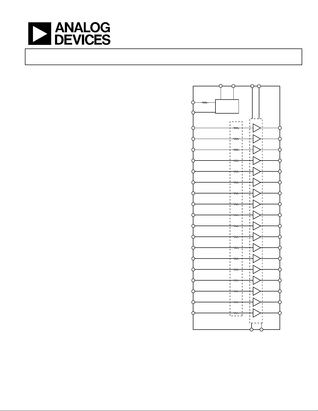
The ADD8709 is an 18-channel integrated gamma reference for
use in LCD TV and monitors panels. The output buffers feature
high current drive and low offset voltage to provide an accurate
and stable gamma curve. The top nine channels swing to V
and the lower nine channels swing to GND.
An on-board voltage regulator provides a fixed input for the
gamma buffers, isolating the gamma curve from supply ripple.
The ADD8709 is specified over the temperature range of
–40°C to +105°C and comes in a 48-lead, Pb-free, low-profile
quad flat package.
DD
DD
V
REG OUT
with Regulator
FUNCTIONAL BLOCK DIAGRAM
V
GND
DD
700Ω*
FB
18
V
IN
17
V
IN
16
V
IN
15
V
IN
V
14
IN
V
13
IN
V
12
IN
V
11
IN
V
10
IN
V
9
IN
V
8
IN
V
7
IN
V
6
IN
V
5
IN
V
4
IN
V
3
IN
V
2
IN
V
1
IN
VOLTAGE
REGULATOR
700Ω*
700Ω*
700Ω*
700Ω*
700Ω*
700Ω*
700Ω*
700Ω*
700Ω*
700Ω*
700Ω*
700Ω*
700Ω*
700Ω*
700Ω*
700Ω*
700Ω*
700Ω*
ADD8709
VDDV
DD
GAMMA
BUFFERS
V
18
OUT
V
17
OUT
V
16
OUT
V
15
OUT
V
14
OUT
V
13
OUT
V
12
OUT
V
11
OUT
V
10
OUT
V
9
OUT
V
8
OUT
V
7
OUT
V
6
OUT
V
5
OUT
V
4
OUT
V
3
OUT
V
2
OUT
V
1
OUT
Rev. A
Information furnished by Analog Devices is believed to be accurate and reliable.
However, no responsibility is assumed by Analog Devices for its use, nor for any
infringements of patents or other rights of third parties that may result from its use.
Specifications subject to change without notice. No license is granted by implication
or otherwise under any patent or patent rights of Analog Devices. Trademarks and
registered trademarks are the property of their respective owners.
*ESD PROTECTION RESISTORS
GND GND
Figure 1. 48-Lead LQFP
One Technology Way, P.O. Box 9106, Norwood, MA 02062-9106, U.S.A.
Tel: 781.329.4700
Fax: 781.326.8703 © 2004 Analog Devices, Inc. All rights reserved.
www.analog.com
04715-001
Page 2

ADD8709
TABLE OF CONTENTS
Electrical Characteristics................................................................. 3
Absolute Maximum Ratings............................................................ 4
ESD Caution.................................................................................. 4
Pin Configuration and Function Descriptions............................. 5
Typical Performance Characteristics ............................................. 7
Application Notes ........................................................................... 10
Volt a ge R e gu l ator ....................................................................... 10
Maximum Power Dissipation ...................................................10
Operating Temperature Range ................................................. 10
Typical Applications Ci r c u it ..........................................................12
Outline Dimensions ....................................................................... 13
Ordering Guide........................................................................... 13
REVISION HISTORY
10/04—Data Sheet Changed from Rev. 0 to Rev. A
Changes to Product Overview Section .......................................... 1
Changes to Figure 1.......................................................................... 1
Changes to Electrical Characteristics Section .............................. 3
Changes to Absolute Maximum Ratings Section......................... 4
Changes to Pin Configuration and Function Description.......... 5
Changes to Typical Performance Characteristics Section........... 7
Changes to Applications Notes Section....................................... 10
Changes to Figure 28, Typical Applications Circuit................... 12
Changes to Ordering Guide.......................................................... 13
8/04—Revision 0: Initial Version
Rev. A | Page 2 of 16
Page 3

ADD8709
ELECTRICAL CHARACTERISTICS
VDD = 16 V, TA @ 25°C, unless otherwise noted.
Table 1.
Parameter Symbol Conditions Min Typ Max Unit
BUFFER CHARACTERISTICS
OUTPUTS
Output Voltage Range (Ch18 to Ch10) V
Output Voltage Range (Ch9 to Ch1) V
Output vs. Load (Ch18, Ch17, Ch2, Ch1) ∆V
Output vs. Load (Ch16 to Ch3) ∆V
OUT
OUT
OUT
OUT
INPUTS
Offset Voltage V
OS
Offset Voltage Drift ∆VOS/∆T
Input Bias Current I
Input Voltage Range (Ch18 to Ch10) V
Input Voltage Range (Ch9 to Ch1) V
B
IN
IN
DYNAMIC PERFORMANCE
Slew Rate SR RL = 10 kΩ, CL = 200 pF 4 6 V/µs
Bandwidth BW –3 dB, RL = 10 kΩ, CL = 200 pF 4.5 MHz
Settling Time to 0.1% t
Phase Margin Ф
S
o
Power Supply Rejection Ratio PSRR VDD = 7 V to 17 V, −40°C ≤ TA ≤ +105°C 68 90 dB
VOLTAGE REGULATOR
Programmable Range V
Initial Regulator Accuracy V
Dropout Voltage V
REG OUT
ACC
DO
I
Line Regulation REG
Load Regulation REG
Maximum Load Current I
Feedback Reference Voltage V
Feedback Input Bias Current I
LINE
LOADIO
O
REF
BFB
POWER SUPPLY
Supply Voltage V
Supply Current I
S
SY
1
∆V
is the shift from the desired output voltage under the specified current load.
OUT
IL = 100 µA 1.4 V
IL = 100 µA 0
1
IL = 20 mA 15 mV
1
IL = 5 mA 5 mV
DD
V
DD
− 1.4
V
V
5 15 mV
−40°C ≤ T
≤ +105°C
A
20 µV/°C
−40°C ≤ TA ≤ +105°C 0.5 1.5 µA
1.4 V
0
V
DD
− 1.4
DD
V
V
1 V step, RL = 10 kΩ, CL = 200 pF 1.1 µs
RL = 10 kΩ, CL = 200 pF 55 Degrees
5
No load; V
= 14.4 V 0.4 1.5 %
REG OUT
V
− 0.6
DD
V
IL = 100 µA 100 150 mV
= 5 mA 310 350 mV
L
VIN = 8.5 V to 16.5 V, V
= 8 V 0.01 0.20 %/V
OUT
= 100 µA to 10 mA 0.02 0.10 %/mA
−40°C ≤ TA ≤ +105°C 5 mA
1.2 V
−40°C ≤ TA ≤ +105°C −150 10 150 nA
7.5 16.5 V
No load, −40°C ≤ TA ≤ +105°C 10.5 17 mA
Rev. A | Page 3 of 16
Page 4
ADD8709
ABSOLUTE MAXIMUM RATINGS
Table 2.
Parameter Rating
Supply Voltage (VDD) 18 V
Input Voltage –0.5 V to V
Storage Temperature Range –65°C to +150°C
Operating Temperature Range
Junction Temperature Range –65°C to +150°C
Lead Temperature Range (Soldering, 60 sec) 300°C
ESD Tolerance (HBM) ±2000 V
ESD Tolerance (MM) ±150 V
1
−40°C to +105°C
DD
Table 3. Package Characteristics
Package Type θ
LQFP (ST) 74.57 °C/W
JA
Unit
1
See section. Application Notes
Stresses above those listed under Absolute Maximum Ratings
may cause permanent damage to the device. This is a stress
rating only; functional operation of the device at these or any
other conditions above those indicated in the operational
sections of this specification is not implied. Exposure to
absolute maximum rating conditions for extended periods
may affect device reliability.
ESD CAUTION
ESD (electrostatic discharge) sensitive device. Electrostatic charges as high as 4000 V readily accumulate on
the human body and test equipment and can discharge without detection. Although this product features
proprietary ESD protection circuitry, permanent damage may occur on devices subjected to high energy
electrostatic discharges. Therefore, proper ESD precautions are recommended to avoid performance
degradation or loss of functionality.
Rev. A | Page 4 of 16
Page 5
ADD8709
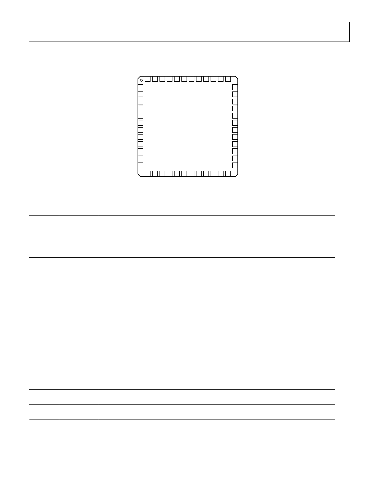
PIN CONFIGURATION AND FUNCTION DESCRIPTIONS
18
17
16
15
14
48 47 46 45 44 43 42 41 40 39 38 37
1
REG
FB
2
GND
3
V
DD
REG OUT
VIN18
VIN17
V
IN
V
IN
V
IN
V
IN
V
IN
V
IN
4
5
6
7
16
8
15
9
14
10
13
11
12
12
11
13 14 15 16 17 18 19 20 21 22 23 24
V
Figure 2. 48-Lead Low-Profile Quad Flat Package (ST-48)
Table 4. Pin Function Descriptions
Pin No. Name Description
1 REG
FB
Regulator feedback. Compares a percentage of the regulator output to the internal 1.2 V voltage
reference.
2 GND Ground. Normally 0 V.
3 V
DD
4 REG
OUT
Supply voltage. Normally 16 V.
Regulator output voltage. Provides a regulated output voltage for use as a reference for the gamma
resistors.
5 VIN18
6 VIN17
7 VIN16
8 VIN15
9 VIN14
10 VIN13
11 VIN12
12 VIN11
13 VIN10
14 VIN9
Buffer inputs. An external resistor calculator is available upon request from your local sales office.
15 VIN8
16 VIN7
17 VIN6
18 VIN5
19 VIN4
20 VIN3
21 VIN2
22 VIN1
23 GND Ground. Normally 0 V.
24 V
25 V
26 V
DD
OUT
OUT
1
2
Supply voltage. Normally 16 V.
Buffer outputs. These buffers can swing to ground.
VDDGND
9
10
IN
IN
V
V
8
V
OUT
IN
OUT
OUT
V
V
ADD8709
TOP VIEW
(Not to Scale)
7
6
IN
IN
V
V
V
5
V
OUT
IN
V
4
V
OUT
IN
13
V
3
V
OUT
IN
12
11
DD
OUT
GND
1
IN
V
V
GND
V
V
OUT
DD
36
V
10
OUT
35
V
9
OUT
34
8
V
OUT
33
7
V
OUT
32
V
DD
31
GND
30
6
V
OUT
29
5
V
OUT
28
4
V
OUT
27
3
V
OUT
26
2
V
OUT
25
V
1
OUT
04715-002
V
2
IN
V
Rev. A | Page 5 of 16
Page 6

ADD8709
Pin No. Name Description
27 V
28 V
29 V
30 V
31 GND Ground. Normally 0 V.
32 V
33 V
34 V
35 V
36 V
37 V
38 V
39 GND Ground. Normally 0 V.
40 V
41 V
42 V
43 V
44 V
45 V
46 V
47 GND Ground. Normally 0 V.
48 V
OUT
OUT
OUT
OUT
DD
OUT
OUT
OUT
OUT
OUT
OUT
DD
OUT
OUT
OUT
OUT
OUT
OUT
DD
3
4
5
6
7
8
9
10
11
12
13
14
15
16
17
18
Buffer outputs. These buffers can swing to ground.
Supply voltage. Normally 16 V.
Buffer outputs. These buffers can swing to ground.
Buffer outputs. These buffers can swing to V
Supply Voltage. Normally 16V.
Buffer outputs. These buffers can swing to V
Supply voltage. Normally 16 V.
.
DD
.
DD
Rev. A | Page 6 of 16
Page 7

ADD8709
TYPICAL PERFORMANCE CHARACTERISTICS
20
15
10
5
0
–5
–10
–15
–20
–25
OUTPUT VOLTAGE ERROR (mV)
–30
–35
–20–100 102030405060708090100110120
I
SOURCE
I
SINK
= 25mA
I
= 25mA
SINK
= 15mA
I
SOURCE
TEMPERATURE (°C)
= 15mA
I
LOAD
= 0mA
I
SOURCE
I
SINK
= 5mA
= 5mA
Figure 3. Output Voltage Error vs. Temperature
30
25
CH17 SOURCE
20
15
10
OUTPUT VOLTAGE ERROR (mV)
5
0
0.1 1 10 100
CH18 SOURCE
CH18 SINK
CH17 SINK
LOAD CURRENT (mA)
Figure 4. Output Voltage Error vs. Load Current (Channels 17 and 18)
30
25
20
15
10
OUTPUT VOLTAGE ERROR (mV)
5
0
0.1 1 10 100
CH10 SOURCE
CH16 SOURCE
LOAD CURRENT (mA)
CH10 SINK
CH16 SINK
Figure 5. Output Voltage Error vs. Load Current (Channels 10 and 16)
04715-003
04715-004
04715-005
25
20
CH3 SOURCE
15
10
5
OUTPUT VOLTAGE ERROR (mV)
0
0.1 1 10 100
LOAD CURRENT (mA)
CH3 SINK
CH9 SOURCE
CH9 SINK
Figure 6. Output Voltage Error vs. Load Current (Channels 3 and 9)
25
20
CH1 SOURCE
15
10
5
OUTPUT VOLTAGE ERROR (mV)
0
0.1 1 10 100
LOAD CURRENT (mA)
CH1 SINK
CH2 SOURCE
CH2 SINK
Figure 7. Output Voltage Error vs. Load Current (Channels 1 and 2)
1000
900
800
700
600
500
400
300
NUMBER OF AMPLIFIERS
200
100
0
–0.30 –0.18 –0.10 –0.02 0.06 0.14 0.22 0.30
GAMMA OUTPUT ERROR DUE TO OFFSET (% OF FS)
Figure 8. Gamma Output Voltage Error
04715-006
04715-007
04715-009
Rev. A | Page 7 of 16
Page 8

ADD8709
11
10
9
8
7
6
5
4
AMPLITUDE (V)
3
2
1
0
–200 180016001400120010008006004002000
TIME (ns)
Figure 9. Gamma Buffers Load Transient Response vs. Capacitive Loading
15
14
13
12
11
10
9
8
7
6
5
OUTPUT VOLTAGE (V)
4
3
2
1
0
17 012345678910111213141516
INPUT VOLTAGE (V)
I
LOAD
I
LOAD
= 10mA
= 0mA
Figure 10. Dropout Characteristics
0
100
200
300
400
500
600
700
DROPOUT VOLTAGE (mV)
800
900
1000
0 1 2 3 4 5 6 7 8 9 10 11 12 13 14 15 16 17 18 19 20
OUTPUT CURRENT (mA)
I
LOAD
10V PULSE
120pF
320pF
520pF
1nF
10nF
= 5mA
04715-008
04715-011
04715-012
800
750
700
650
600
550
500
450
400
350
300
250
200
DROPOUT VOLTAGE (mV)
150
100
50
0
–25–15–5 5 152535455565758595105115
TEMPERATURE (°C)
10mA
5mA
0mA
Figure 12. Dropout Voltage vs. Temperature
14.5
14.4
14.3
14.2
14.1
14.0
13.9
REGULATOR OUTPUT (V)
13.8
13.7
13.6
0 2 4 6 8 10 12 14 16 18 20
Figure 13. Regulator Output vs. I
14.45
14.40
14.35
14.30
REGULATOR OUTPUT (V)
14.25
14.20
–20–100 102030405060708090100110
+25°C
+55°C
+85°C
LOAD CURRENT (mA)
over Temperature
LOAD
TEMPERATURE (°C)
+95°C
–20°C
+105°C
0mA
5mA
04715-013
0°C
04715-014
10mA
04715-015
Figure 11. Dropout Voltage vs. Output Current
Figure 14. Regulator Output vs. Temperature
Rev. A | Page 8 of 16
Page 9

ADD8709
18
17
16
INPUT VOLTAGE (V)
15
14
Figure 15. Regulator Line Transient Response
TIME (100µs/DIV)
C
LOAD
= 1µF
400
200
0
–200
–400
OUTPUT VOLTAGE CHANGE (mV)
04715-016
12
11
10
9
8
7
6
5
4
SUPPLY CURRENT (mA)
3
2
1
0
0 2 4 6 8 10 12 14 16 18
SUPPLY VOLTAGE (V)
Figure 17. Supply Current vs. Supply Voltage
04715-018
0.1
LOAD CURRENT (mA)
5
C
= 1µF
LOAD
TIME (100µs/DIV)
Figure 16. Regulator Load Transient Response
40
20
0
–20
–40
OUTPUT VOLTAGE CHANGE (mV)
04715-017
11.0
10.9
10.8
10.7
10.6
SUPPLY CURRENT (mA)
10.5
10.4
–20 120100806040200
TEMPERATURE (°C)
04715-019
Figure 18. Supply Current vs. Temperature
Rev. A | Page 9 of 16
Page 10

ADD8709
APPLICATION NOTES
The ADD8709 is a gamma reference generator that allows
source drivers to be optimized for the different combinations
of liquid crystals, glass sizes, etc. in large LCD panels.
In a typical panel application, the selected source drivers have
an internal gamma curve that is not ideal for the specific panel,
as shown in Figure 19. The ADD8709 allows the gamma curve
in the source drivers to be adjusted appropriately, and also
ensures that all of the source drivers have the same gamma
curve.
16
14
12
10
8
6
PANEL GAMMA CURVE
CORRECTED BY ADD8709
GAMMA VOLTAGE (V)
4
2
0
Figure 19. Original and Corrected Gamma Cur ves
The ADD8709 also includes a low dropout linear regulator to
provide a stable reference level for the gamma curve for best
panel performance.
VOLTAGE REGULATOR
The on-board voltage regulator provides a regulated voltage to
the external resistors to set different gamma voltages.
The output of the regulator is set by the two resistors, R
and an internal reference voltage of 1.2V. In the ADD8709, R
and R
are external components. The output voltage can is
2
found by
= V
V
REG OUT
× (R2/R1 + 1)
REF
5kΩ
V
1.2V
ORIGINAL GAMMA CURVE
IN SOURCE DRIVERS
GAMMA REFERENCE INPUT POINTS
R
2
R
REF
Figure 20. Voltage Regulator
55kΩ
1
V
REG OUT
+
–
04715-021
04715-020
and R2,
1
1
MAXIMUM POWER DISSIPATION
The maximum safe power dissipation in the ADD8709 package
is limited by the associated rise in junction temperature (T
) on
J
the die. At approximately 150°C, the glass transition temperature, the properties of the plastic change. Even temporarily
exceeding this temperature limit may change the stresses that
the package exerts on the die, permanently shifting the parametric performance of the ADD8709. Exceeding a junction
temperature of 175°C for an extended period can result in
changes in the silicon devices, potentially causing failure.
OPERATING TEMPERATURE RANGE
The junction temperature is
= T
T
where:
T
AMB
θ
= junction-to-ambient thermal resistance, in °C/watt.
JA
P
DIS
For the ADD8709, P
where:
V
DD
I
OUT X(+)
dissipation (current comes from V
−I
OU XT(-)
dissipation (current goes to GND).
(V
DD
Example 1
To calculate an estimated power consumption of the ADD8709
assume:
+ θJA × P
J
AMB
DIS
= ambient temperature.
= power dissipated in the device, in watts.
can be calculated by
DIS
= VDD × IDQ + Σ(I
P
DIS
Σ(−I
× I
DQ
× (VDD − V
– V
V
DD
(V
OUT X(-)
× V
) + (VDD – V
OUTX
= nominal system power requirements.
) = positive-current amplifier load power
OUT X
× V
= negative-current amplifier load power
OUT X
) × I
REG OUT
= regulator load power dissipation.
LOAD
× IDQ = 16 V × 15 mA = 0.240 W.
– V
DD
REG OUT
) × I
LOAD
× (VDD − V
OUT X(+)
REG OUT
DD
OUT X
) × I
).
= (16 V – 14.4 V) × 5 mA = 0.008 W.
)) +
LOAD
Rev. A | Page 10 of 16
Page 11

ADD8709
P
Table 5.
V
V
18 14.400 4.3 0.00688
OUT
V
17 11.405 5.2 0.0239
OUT
V
16 10.627
OUT
V
15 10.397 7.3 0.0409
OUT
V
14 10.195 7.6 0.0441
OUT
V
13 10.080
OUT
V
12 9.821 8.3 0.0513
OUT
V
11 9.130 7.9 0.0543
OUT
V
10 8.611
OUT
V
9 6.480
OUT
V
8 6.077 5.6 0.0556
OUT
V
7 5.098 -3.3 0.0168
OUT
V
6 4.810
OUT
V
5 4.694 5.7 0.0644
OUT
V
4 4.435 3.5 0.0405
OUT
V
3 4.205 9.6 0.113
OUT
V
2 3.398
OUT
V
1 0.202
OUT
Σ(I
OUT X(+)
(V) I
OUT X
× (VDD − V
OUT X
)) + Σ(−I
(mA) P (W)
OUT X
−4.4
−3.9
−4.5
−4.2
−6.9
−9.5
−7.2
× V
OUT X(-)
OUT X
)
0.0468
0.0393
0.0389
0.0272
0.0332
0.0323
0.00145
0.731
Here, 150°C is the maximum junction temperature that is
guaranteed before the part breaks down, while 125°C is the
maximum process limit. Because T
this example demonstrates a condition where the part should
perform within process limits.
= 0.240 W + 0.731 W + 0.008 W =0.979 W
DIS
= 74.57°C/W, T
θ
JA
= 45°C + (74.57°C/W) × (0.979 W) = 118.0°C
T
J
AMB
= 45°C
is < 150°C and < 125°C,
J
Rev. A | Page 11 of 16
Page 12

ADD8709
TYPICAL APPLICATIONS CIRCUIT
0.1µF
EXTERNAL
RESISTORS
TO SET
GAMMA
VOLTAGES
V
REG OUT
3.12kΩ
2.22kΩ
1.02kΩ
3.33kΩ
5kΩ
55kΩ
0Ω
810Ω
240Ω
210Ω
120Ω
270Ω
720Ω
540Ω
420Ω
300Ω
120Ω
270Ω
240Ω
840Ω
210Ω
700Ω*
FB
14.4V
18
V
IN
17
V
IN
16
V
IN
15
V
IN
14
V
IN
13
V
IN
12
V
IN
11
V
IN
10
V
IN
9
V
IN
8
V
IN
7
V
IN
6
V
IN
5
V
IN
4
V
IN
3
V
IN
2
V
IN
1
V
IN
VOLTAGE
REGULATOR
700Ω*
700Ω*
700Ω*
700Ω*
700Ω*
700Ω*
700Ω*
700Ω*
700Ω*
700Ω*
700Ω*
700Ω*
700Ω*
700Ω*
700Ω*
700Ω*
700Ω*
700Ω*
V
DD
16V
0.1µF
GAMMA 18
GAMMA 17
GAMMA 16
GAMMA 15
GAMMA 14
+
1.2V
–
GAMMA
BUFFERS
V
18
OUT
V
OUT
V
OUT
V
OUT
V
OUT
V
OUT
V
OUT
V
OUT
V
OUT
V
OUT
V
OUT
V
OUT
V
OUT
V
OUT
V
OUT
V
OUT
V
OUT
V
OUT
14.400V
17
11.405V
16
10.627V
15
10.397V
14
10.195V
13
10.080V
12
9.821V
11
9.130V
10
8.611V
9
6.480V
8
6.077V
7
5.098V
6
4.810V
5
4.694V
4
4.435V
3
4.205V
2
3.398V
1
0.202V
GAMMA 13
GAMMA 12
GAMMA 11
GAMMA 10
GAMMA 9
GAMMA 8
GAMMA 7
GAMMA 6
GAMMA 5
GAMMA 4
GAMMA 3
GAMMA 2
GAMMA 1
GAMMA 18
GAMMA 17
GAMMA 16
GAMMA 15
GAMMA 14
GAMMA 13
GAMMA 12
GAMMA 11
GAMMA 10
GAMMA 9
GAMMA 8
GAMMA 7
GAMMA 6
GAMMA 5
GAMMA 4
GAMMA 3
GAMMA 2
GAMMA 1
GAMMA 18
GAMMA 17
GAMMA 16
GAMMA 15
GAMMA 14
GAMMA 13
GAMMA 12
GAMMA 11
GAMMA 10
GAMMA 9
GAMMA 8
GAMMA 7
GAMMA 6
GAMMA 5
GAMMA 4
GAMMA 3
GAMMA 2
GAMMA 1
*ESD PROTECTION RESISTORS
GND GND
Figure 21. Typical Applications Circuit
Rev. A | Page 12 of 16
04715-022
Page 13

ADD8709
OUTLINE DIMENSIONS
ORDERING GUIDE
1
Model
ADD8709ASTZ-REEL
ADD8709ASTZ-REEL7
ADD8709WSTZ-REEL2
ADD8709WSTZ-REEL72
2, 3
1.45
1.40
1.35
0.15
SEATING
0.05
PLANE
VIEW A
ROTATED 90° CCW
0.75
0.60
0.45
0.20
0.09
7°
3.5°
0°
0.08 MAX
COPLANARITY
COMPLIANT TO JEDEC STANDARDS MS-026BBC
1.60
MAX
VIEW A
LEAD PITCH
1
12
0.50
BSC
48
13
9.00 BSC
SQ
PIN 1
TOP VIEW
(PINS DOWN)
37
36
7.00
BSC SQ
25
24
0.27
0.22
0.17
Figure 22. 48-Lead Low Profile Quad Flat Package [LQFP]
(ST-48)
Dimensions shown in millimeters
Temperature Range Package Description Package Option
−40°C to +100°C
2, 3
−40°C to +100°C
−40°C to +105°C
−40°C to +105°C
48-Lead Low Profile Quad Flat Package ST-48
48-Lead Low Profile Quad Flat Package ST-48
48-Lead Low Profile Quad Flat Package ST-48
48-Lead Low Profile Quad Flat Package ST-48
1
Available in reels only.
2
Z = Pb-free part.
3
WARNING: Not to be used in new design. Option for existing designs only.
Rev. A | Page 13 of 16
Page 14

ADD8709
NOTES
Rev. A | Page 14 of 16
Page 15

ADD8709
NOTES
Rev. A | Page 15 of 16
Page 16

ADD8709
NOTES
© 2004 Analog Devices, Inc. All rights reserved. Trademarks and
registered trademarks are the property of their respective owners.
D04715–0–10/04(A)
Rev. A | Page 16 of 16
 Loading...