

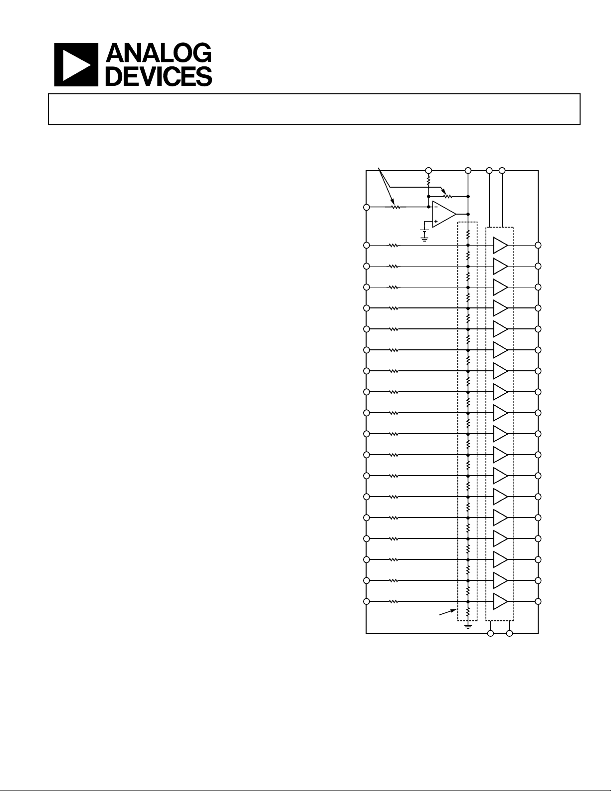
18-Channel Gamma Buffer
FEATURES
18 precision gamma reference outputs
Mask-programmable gamma resistors:
0.2% resolution and 0.1% accuracy
Mask-programmable voltage regulator: 0.4% accuracy
Upper 9 buffers swing to V
Lower 9 buffers swing to GND
Single-supply operation: 7.5 V to 16.5 V
Gamma current drive: 15 mA per channel
Peak output current: 150 mA
Output voltage stable under load conditions
Pin-to-pin compatible with ADD8709
48-lead, Pb-free LQFP and LFCSP
APPLICATIONS
LCD TV panels
LCD monitor panels
GENERAL DESCRIPTION
The ADD8708 is an 18-channel integrated gamma reference for
use in high resolution LCD TV and monitors panels. The output buffers feature high current drive and low offset voltage to
provide an accurate and stable gamma curve. The top nine
channels swing to V
Integrating the gamma setup resistors drastically reduces the
external component count while increasing the gamma curve
accuracy. To accommodate multiple column drivers and panel
architectures, the ADD8708 is mask programmable to a 0.2%
resolution using the on-chip 500 resistor string. An on-board
voltage regulator provides a fixed input for the resistor string,
isolating the gamma curve from the supply ripple.
The ADD8708 is specified over the temperature range of
–40°C to +105°C and comes in both a 48-lead, Pb-free,
lead-frame chip-scale package and a Pb-free, low-profile,
quad flat package.
DD
; the lower nine channels swing to GND.
DD
FUNCTIONAL BLOCK DIAGRAM
MASK-PROGRAMMABLE
REGULATOR RESISTORS
GND
1.2V
18
V
IN
V
17
IN
V
16
IN
V
15
IN
V
14
IN
V
13
IN
V
12
IN
V
11
IN
V
10
IN
V
IN
V
IN
V
IN
V
IN
V
IN
V
IN
V
IN
V
IN
V
IN
700Ω*
700Ω*
700Ω*
700Ω*
700Ω*
700Ω*
700Ω*
700Ω*
700Ω*
700Ω*
9
700Ω*
8
700Ω*
7
700Ω*
6
700Ω*
5
700Ω*
4
700Ω*
3
700Ω*
2
700Ω*
1
MASK-PROGRAMMABLE
RESISTOR STRING
*ESD PROTECTION RESISTORS
Figure 1. 48-Lead LQFP or LFCSP
FB V
700Ω*
+
–
with Regulator
ADD8708
VDDV
REG OUT
DD
GAMMA
BUFFERS
GND GND
V
18
OUT
V
17
OUT
V
16
OUT
V
15
OUT
V
14
OUT
V
13
OUT
V
12
OUT
V
11
OUT
V
10
OUT
V
9
OUT
V
8
OUT
V
7
OUT
V
6
OUT
V
5
OUT
V
4
OUT
V
3
OUT
V
2
OUT
V
1
OUT
04614-001
Rev. 0
Information furnished by Analog Devices is believed to be accurate and reliable.
However, no responsibility is assumed by Analog Devices for its use, nor for any
infringements of patents or other rights of third parties that may result from its use.
Specifications subject to change without notice. No license is granted by implication
or otherwise under any patent or patent rights of Analog Devices. Trademarks and
registered trademarks are the property of their respective owners.
One Technology Way, P.O. Box 9106, Norwood, MA 02062-9106, U.S.A.
Tel: 781.329.4700
Fax: 781.326.8703 © 2004 Analog Devices, Inc. All rights reserved.
www.analog.com

ADD8708
TABLE OF CONTENTS
Electrical Characteristics................................................................. 3
Absolute Maximum Ratings............................................................ 4
ESD Caution.................................................................................. 4
Pin Configuration and Function Descriptions............................. 5
Typical Performance Characteristics ............................................. 7
Application Notes ........................................................................... 10
Tap Point Selection..................................................................... 10
Volt a ge R e gu l ator ....................................................................... 11
Maximum Power Dissipation ...................................................11
Land Pattern................................................................................ 11
Operating Temperature Range ................................................. 12
Typical Applications Ci r c u it ..........................................................14
Tap Point and Regulator Voltage Request Form......................... 15
Outline Dimensions ....................................................................... 16
Ordering Guide........................................................................... 16
REVISION HISTORY
10/04—Revision 0: Initial Version
Rev. 0 | Page 2 of 16
ADD8708
ELECTRICAL CHARACTERISTICS
VDD = 16 V, TA @ 25°C, unless otherwise noted.
Table 1.
Parameter Symbol Conditions Min Typ Max Unit
GAMMA CURVE CHARACTERISTICS
Accuracy R
Programming Resolution R
Total Resistor String R
BUFFER CHARACTERISTICS
OUTPUTS
Output Voltage Range (Ch18 to Ch10) V
Output Voltage Range (Ch9 to Ch1) V
Output vs. Load (Ch18, Ch17, Ch2, Ch1) ∆V
Output vs. Load (Ch16 to Ch3) ∆V
INPUTS
Offset Voltage V
Offset Voltage Drift ∆VOS/∆T
Input Bias Current I
Input Voltage Range (Ch18 to Ch10) V
Input Voltage Range (Ch9 to Ch1) V
DYNAMIC PERFORMANCE
Slew Rate SR RL = 10 kΩ, CL = 200 pF 4 6 V/µs
Bandwidth BW –3 dB, RL = 10 kΩ, CL = 200 pF 4.5 MHz
Settling Time to 0.1% t
Phase Margin Ф
Power Supply Rejection Ratio PSRR
VOLTAGE REGULATOR
Programmable Range V
Initial Regulator Accuracy V
Dropout Voltage V
I
Line Regulation REG
Load Regulation REG
Maximum Load Current I
Feedback Reference Voltage V
Feedback Input Bias Current I
SYSTEM ACCURACY
Total Error
3, 4
POWER SUPPLY
Supply Voltage V
Supply Current I
ACC
RES
TOTAL
OUT
OUT
OUT
OUT
OS
B
IN
IN
S
o
REG OUT
ACC
DO
O
REF
B FB
V
Total Error
DD
SY
1
2
2
LINE
LOADIO
0.1 0.4 %
500 segments 0.2 %
15 kΩ
IL = 100 µA 1.4 V
IL = 100 µA 0
DD
V
− 1.4
DD
V
V
IL = 20 mA 15 mV
IL = 5 mA 5 mV
5 15 mV
−40°C ≤ T
≤ +105°C
A
−40°C ≤ TA ≤ +105°C
1.4 V
0
20 µV/°C
0.5 1.5 µA
DD
V
− 1.4
DD
V
V
1 V, RL = 10 kΩ, CL = 200 pF 1.1 µs
RL = 10 kΩ, CL = 200 pF 55 Degrees
= 7 V to 17 V,
V
DD
−40°C ≤ T
≤ +105°C
A
5
No load; V
= 14.4V 0.4 1.5 %
REG OUT
68 90 dB
V
− 0.6
DD
V
IL = 100 µA 100 150 mV
= 5 mA 310 350 mV
L
VIN = 8.5 V to 16.5 V, V
= 8 V 0.01 0.20 %/V
OUT
= 100 µA to 10 mA 0.02 0.10 %/mA
−40°C ≤ TA ≤ +105°C
−40°C ≤ TA ≤ +105°C
−40°C ≤ TA ≤ +105°C
5 mA
1.2 V
-150 10 150 nA
0.5 3 %
7.5 16 V
No load; −40°C ≤ TA ≤ +105°C
9.5 16 mA
1
Gamma curve accuracy includes resistor matching and buffer errors, but excludes the regulator error.
2
∆V
is the shift from the desired output voltage under the specified current load.
OUT
3
Total error is the difference between the designed and actual output voltage divided by the actual regulator output voltage or full-scale voltage.
4
Total error includes regulator error, resistor string error, bias current effects, and buffer offset voltage.
Rev. 0 | Page 3 of 16
ADD8708
ABSOLUTE MAXIMUM RATINGS
Table 2.
Parameter Rating
Supply Voltage (VDD) 18 V
Input Voltage
Storage Temperature Range
Operating Temperature Range
1
−0.5 V to V
DD
−65°C to +150°C
−40°C to +105°C
Junction Temperature Range –65°C to +150°C
Lead Temperature Range (Soldering, 60 sec) 300°C
ESD Tolerance (HBM) ±1500 V
ESD Tolerance (MM) ±200 V
Table 3. Package Characteristics
Package Type θ
2
JA
3
θ
JA
Unit
LFCSP (CP) 28.3 47.7 °C/W
LQFP (ST) N/A 74.57 °C/W
1
See the section. Application Notes
2
θJA for exposed pad soldered to JEDEC 4-layer board.
3
θJA for exposed pad not soldered down.
Stresses above those listed under Absolute Maximum Ratings
may cause permanent damage to the device. This is a stress
rating only; functional operation of the device at these or any
other conditions above those indicated in the operational
sections of this specification is not implied. Exposure to
absolute maximum rating conditions for extended periods may
affect device reliability.
ESD CAUTION
ESD (electrostatic discharge) sensitive device. Electrostatic charges as high as 4000 V readily accumulate on
the human body and test equipment and can discharge without detection. Although this product features
proprietary ESD protection circuitry, permanent damage may occur on devices subjected to high energy
electrostatic discharges. Therefore, proper ESD precautions are recommended to avoid performance
degradation or loss of functionality.
Rev. 0 | Page 4 of 16
ADD8708
PIN CONFIGURATION AND FUNCTION DESCRIPTIONS
18
17
16
15
14
REG
V
REG OUT
GND
V
VIN18
V
IN
V
IN
V
IN
V
IN
V
IN
V
IN
V
IN
OUT
OUT
OUT
OUT
VDDGND
V
48 47 46 45 44 43 42 41 40 39 38 37
1
FB
2
3
DD
4
5
17
6
16
7
15
8
14
9
13
10
12
11
11
12
13 14 15 16 17 18 19 20 21 22 23 24
10
IN
V
9
8
7
IN
IN
IN
V
V
V
OUT
V
V
V
ADD8708
TOP VIEW
(Not to Scale)
6
5
4
IN
IN
IN
V
V
V
Figure 2. Pin Configuration
13
V
3
V
OUT
IN
12
11
DD
OUT
OUT
GND
V
V
2
IN
V
V
36
V
10
OUT
35
9
V
OUT
34
8
V
OUT
33
7
V
OUT
32
V
DD
GND
31
6
V
30
OUT
5
V
29
OUT
V
4
28
OUT
3
V
27
OUT
2
V
26
OUT
1
V
25
OUT
1
DD
IN
V
V
GND
04614-002
Table 4. Pin Function Descriptions
Pin No. Name Description
1 REG
FB
Regulator Feedback. Compares a percentage of the regulator output to the internal 1.2 V voltage
reference. Internal resistors are used to program the desired regulator output voltage.
2 GND Ground. Normally 0 V.
3 V
4 V
DD
REG OUT
Supply Voltage. Normally 16 V.
Regulator output voltage. Provides reference voltage to resistor string and is internally connected to
the top of the resistor string.
5 VIN18
6 VIN17
7 VIN16
8 VIN15
9 VIN14
10 VIN13
11 VIN12
12 VIN11
13 VIN10
14 VIN9
Buffer inputs. Normally floating.
1
15 VIN8
16 VIN7
17 VIN6
18 VIN5
19 VIN4
20 VIN3
21 VIN2
22 VIN1
23 GND Ground. Normally 0 V.
24 V
DD
Supply Voltage. Normally 16 V.
1
External resistors can be added to modify the internal resistor string to change the gamma voltage. An external resistor calculator is available upon request from your
local sales office.
Rev. 0 | Page 5 of 16

ADD8708
Pin No. Name Description
25 V
26 V
27 V
28 V
29 V
30 V
31 GND Ground. Normally 0 V.
32 V
33 V
34 V
35 V
36 V
37 V
38 V
39 GND Ground. Normally 0 V.
40 V
41 V
42 V
43 V
44 V
45 V
46 V
47 GND Ground. Normally 0 V.
48 V
OUT
OUT
OUT
OUT
OUT
OUT
DD
OUT
OUT
OUT
OUT
OUT
OUT
DD
OUT
OUT
OUT
OUT
OUT
OUT
DD
1
2
3
4
5
6
7
8
9
10
11
12
13
14
15
16
17
18
Buffer Outputs. These buffers can swing to ground.
Supply voltage. Normally 16 V.
Buffer Output. These buffers can swing to ground.
Buffer Output. These buffers can swing to VDD.
Normally 16 V.
Buffer Outputs. These buffers can swing to V
Supply voltage. Normally 16 V.
.
DD
Rev. 0 | Page 6 of 16
ADD8708
TYPICAL PERFORMANCE CHARACTERISTICS
20
15
10
5
0
–5
–10
–15
–20
–25
OUTPUT VOLTAGE ERROR (mV)
–30
–35
–20–100 102030405060708090100110120
I
SOURCE
I
SINK
= 25mA
I
= 25mA
SINK
I
= 15mA
SOURCE
TEMPERATURE (°C)
= 15mA
I
LOAD
I
= 0mA
I
SOURCE
SINK
= 5mA
= 5mA
Figure 3. Output Voltage Error vs. Temperature
30
04614-003
25
20
CH3 SOURCE
15
10
5
OUTPUT VOLTAGE ERROR (mV)
0
0.1 1 10 100
LOAD CURRENT (mA)
CH3 SINK
CH9 SOURCE
CH9 SINK
Figure 6. Output Voltage Error vs. Load Current (Channels 3 and 9)
25
04614-006
25
CH17 SOURCE
20
15
10
OUTPUT VOLTAGE ERROR (mV)
5
0
0.1 1 10 100
CH18 SOURCE
CH18 SINK
CH17 SINK
LOAD CURRENT (mA)
Figure 4. Output Voltage Error vs. Load Current (Channels 17 and 18)
30
25
20
15
10
OUTPUT VOLTAGE ERROR (mV)
5
0
0.1 1 10 100
CH10 SOURCE
CH16 SOURCE
LOAD CURRENT (mA)
CH10 SINK
CH16 SINK
Figure 5. Output Voltage Error vs. Load Current (Channels 10 and 16)
04614-004
04614-005
20
CH1 SOURCE
15
10
5
OUTPUT VOLTAGE ERROR (mV)
0
0.1 1 10 100
LOAD CURRENT (mA)
CH1 SINK
CH2 SOURCE
CH2 SINK
04614-007
Figure 7. Output Voltage Error vs. Load Current (Channels 1 and 2)
AMPLITUDE (V)
11
10
9
8
7
6
5
4
3
2
1
0
–200 180016001400120010008006004002000
TIME (ns)
10V PULSE
120pF
320pF
520pF
1nF
10nF
04614-008
Figure 8. Gamma Buffers Transient Load Response vs. Capacitive Loading
Rev. 0 | Page 7 of 16

ADD8708
1000
900
800
700
600
500
400
300
NUMBER OF AMPLIFIERS
200
100
0
–0.30 –0.18 –0.10 –0.02 0.06 0.14 0.22 0.30
0.3
MAX ERROR EACH STEP
0.2
0.1
0
ERROR (%)
–0.1
–0.2
–0.3
0123456789101112
Figure 10. Gamma Output Error per Channel (920 Parts)
15
14
13
12
11
10
9
8
7
6
5
OUTPUT VOLTAGE (V)
4
3
2
1
0
17 012345678910111213141516
GAMMA OUTPUT ERROR DUE TO OFFSET AND
RESISTOR MATCHING (% OF FS)
Figure 9. Gamma Output Voltage Error
TYPICAL UNIT B
TYPICAL UNIT A
OUTPUT CHANNEL
TYPICAL UNIT C
MIN ERROR EACH STEP
I
= 0mA
LOAD
I
= 5mA
LOAD
= 10mA
I
LOAD
INPUT VOLTAGE (V)
04614-009
04614-010
04614-011
0
100
200
300
400
500
600
700
DROPOUT VOLTAGE (mV)
800
900
1000
01234567891011121314151617181920
OUTPUT CURRENT (mA)
Figure 12. Dropout Voltage vs. Output Current
800
750
700
650
600
550
500
450
400
350
300
250
200
DROPOUT VOLTAGE (mV)
150
100
50
0
–25–15–55 152535455565758595105115
TEMPERATURE (°C)
10mA
5mA
0mA
Figure 13. Dropout Voltage vs. Temperature
14.5
14.4
14.3
14.2
14.1
14.0
13.9
REGULATOR OUTPUT (V)
13.8
13.7
13.6
0 2 4 6 8 101214161820
+25°C
°
C
+55
+85
LOAD CURRENT (mA)
°
C
+95
°
C
+105
–20°C
°
C
04614-012
04614-013
0
°
C
04614-014
Figure 11. Dropout Characteristics
Rev. 0 | Page 8 of 16
Figure 14. Regulator Output vs. I
over Temperature
LOAD

ADD8708
14.45
0mA
14.40
14.35
14.30
REGULATOR OUTPUT (V)
14.25
14.20
–20–100 102030405060708090100110
TEMPERATURE (°C)
5mA
Figure 15. Regulator Output vs. Temperature
18
17
C
LOAD
= 1µF
10mA
04712-0-021
400
200
12
11
10
9
8
7
6
5
4
SUPPLY CURRENT (mA)
3
2
1
0
024681012141618
SUPPLY VOLTAGE (V)
Figure 18. Supply Current vs. Supply Voltage
11.0
10.9
10.8
04614-018
16
INPUT VOLTAGE (V)
15
14
0.1
LOAD CURRENT (mA)
5
TIME (100µs/DIV)
Figure 16. Regulator Line Transient Response
C
= 1µF
LOAD
TIME (100µs/DIV)
0
–200
–400
40
20
0
–20
–40
OUTPUT VOLTAGE CHANGE (mV)
OUTPUT VOLTAGE CHANGE (mV)
04614-016
04614-017
10.7
10.6
SUPPLY CURRENT (mA)
10.5
10.4
–20 120100806040200
TEMPERATURE (°C)
Figure 19. Supply Current vs. Temperature
04614-019
Figure 17. Regulator Load Transient Response
Rev. 0 | Page 9 of 16

ADD8708
V
APPLICATION NOTES
The ADD8708 is a mask-programmable gamma reference
generator that allows source drivers to be optimized for the
different combinations of liquid crystals, glass sizes, etc. in
large LCD panels. It generates 18 gamma reference outputs
that can be mask-programmed in 0.2% increments using the
500 matched internal resistors (see Figure 20), so that every
point on the curve can be targeted within 0.1% of the desired
value.
TAP POINT 4
TAP POINT 3
TAP POINT 2
TAP POINT 1
EACH R = 30Ω
TYPICALLY
Figure 20. 500 Mask-Programmable Resistor String
In a typical panel application, the selected source drivers have
an internal gamma curve that is not ideal for the specific panel
(see Figure 21). The ADD8708 allows the gamma curve in the
source drivers to be adjusted appropriately, and also ensures
that all the source drivers have the same gamma curve.
16
14
12
10
8
6
PANEL GAMMA CURVE
CORRECTED BY ADD8708
GAMMA VOLTAGE (V)
4
2
0
ORIGINAL GAMMA CURVE
IN SOURCE DRIVERS
GAMMA REFERENCE INPUT POINTS
Figure 21. Original and Corrected Gamma Cur ves
The matching and tracking accuracy of the internal resistors is
typically 0.1% with worst-case deviation from the desired curve
within 0.4% of the ideal gamma curve, over temperature.
The ADD8708 also includes a low-dropout linear regulator to
provide a stable reference level for the gamma curve for
optimum panel performance.
TAP POINT 500
TAP POINT 499
TAP POINT 498
TAP POINT 497
04614-020
04614-021
TAP POINT SELECTION
The ADD8708 uses a single resistor string consisting of 500
individual elements. The tap points are mask programmable
and completely independent of each other. See the Tap Point
and Regulator Voltage Request Form in this data sheet.
V
REG OUT
500–TP
X
IN
X
TP
X
Figure 22. Gamma Buffers Tap Point Circuit
Tap point voltages can be derived from the following equation:
OUT
500
TP
X
XV ×=
where TP
is the desired tap point for the Xth channel.
X
Table 5. Typical Mask Implementation
VDD = 16 V, V
= 14.4 V, 0 ≤ X ≤ 500
REG OUT
Tap Point (X) Voltage Units
V
18 500 14.400 V
OUT
V
17 396 11.405 V
OUT
V
16 369 10.627 V
OUT
V
15 361 10.397 V
OUT
V
14 354 10.195 V
OUT
V
13 350 10.080 V
OUT
V
12 341 9.821 V
OUT
V
11 317 9.130 V
OUT
V
10 299 8.611 V
OUT
V
9 225 6.480 V
OUT
V
8 211 6.077 V
OUT
V
7 177 5.098 V
OUT
V
6 167 4.810 V
OUT
V
5 163 4.694 V
OUT
V
4 154 4.435 V
OUT
V
3 146 4.205 V
OUT
V
2 118 3.398 V
OUT
V
1 7 0.202 V
OUT
_______________________________
1
ADD8708 release samples do not have these typical values. The values on the
samples are nonmonotonic and can be provided upon request.
V
X
OUT
04614-022
V
OUTREG
1
Rev. 0 | Page 10 of 16
ADD8708
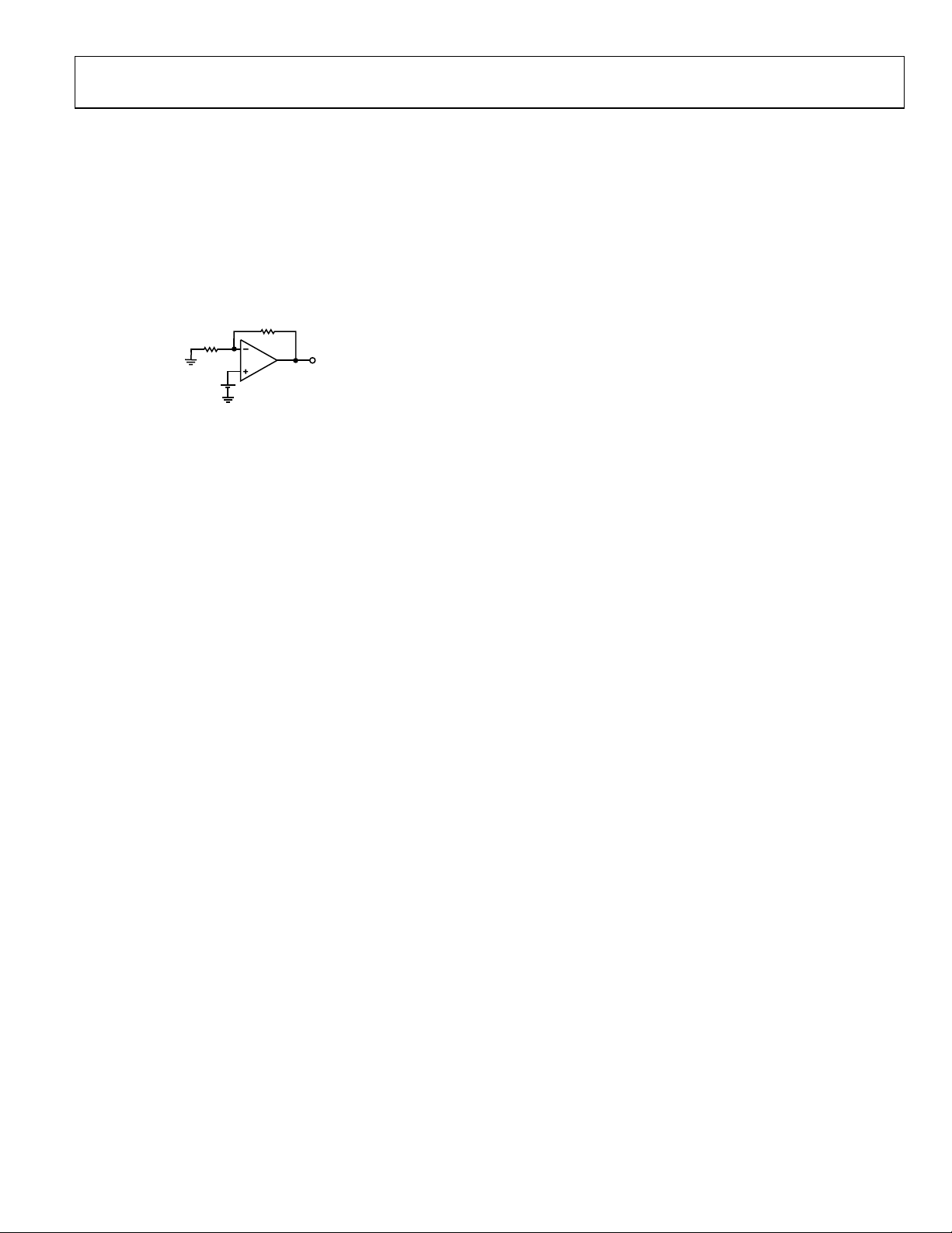
VOLTAGE REGULATOR
The on-board voltage regulator provides a regulated voltage to
the resistor chain to provide stable gamma voltages.
The two mask-programmable internal resistors, R
and R2,
1
and a reference voltage set the output of the regulator. The
typical values of these parts are shown in Figure 23. In addition,
see the Tap Point and Regulator Voltage Request Form in this
data sheet.
R
2
R
5kΩ
V
REF
1.2V
Figure 23. Voltage Regulator
55kΩ
1
V
REG OUT
+
–
04614-023
The internal resistors have a typical accuracy of 0.1%. External
resistors can be used to adjust the regulator voltage; however, it
is not recommended. Please contact your local sales office for
further details.
MAXIMUM POWER DISSIPATION
The maximum safe power dissipation in the ADD8708 package
is limited by the associated rise in junction temperature (T
the die. At approximately 150°C, the glass transition temperature, the properties of the plastic change. Even temporarily
exceeding this temperature limit may change the stresses that
the package exerts on the die, permanently shifting the parametric performance of the ADD8708. Exceeding a junction
temperature of 175°C for an extended period can result in
changes in the silicon devices, potentially causing failure.
) on
J
LAND PATTERN
The LFCSP package comes with a thermal pad. Soldering down
this thermal pad dramatically improves the heat dissipation of
the package. It is necessary to attach vias that connect the
soldered thermal pad to another layer on the board. This
provides an avenue to dissipate the heat away from the part.
Without vias, the heat is isolated directly under the part.
Subdivide the solder paste, or stencil layer, for the thermal pad
to reduce solder balling and splatter. It is not critical how the
subdivisions are arranged, as long as the total coverage of the
solder paste for the thermal pad is greater than 50%. The land
pattern is critical to heat dissipation. A suggested land pattern is
shown in Figure 22.
The thermal pad is attached to the substrate. In the ADD8708,
the substrate is connected to V
. To be electrically safe, the
DD
thermal pad should be soldered to an area on the board that is
electrically isolated or connected to V
. Attaching the thermal
DD
pad to ground adversely affects the performance of the part.
Rev. 0 | Page 11 of 16

ADD8708
OPERATING TEMPERATURE RANGE
The junction temperature is as follows:
= T
T
J
where:
T
AMB
= junction-to-ambient thermal resistance, in °C/watt.
θ
JA
P
= power dissipated in the device, in watts.
DIS
For the ADD8708, P
P
DIS
where:
V
I
OUT X(+)
power dissipation (current comes from V
−I
dissipation (current goes to GND).
(V
In this example, T
values in Table 6.
Table 6.
V
V
OUT
V
OUT
V
OUT
V
OUT
V
OUT
V
OUT
V
OUT
V
OUT
V
OUT
V
OUT
V
OUT
V
OUT
V
OUT
V
OUT
V
OUT
V
OUT
V
OUT
V
OUT
Σ(I
+ θJA × P
AMB
DIS
= ambient temperature.
can be calculated by this equation:
DIS
= VDD × IDQ + Σ(I
Σ(−I
OUT X(−)
× I
DD
= nominal system power requirements.
DQ
× (VDD − V
× V
OUT X(−)
– V
DD
OUT X
REG OUT
OUT X
) × I
AMB
× V
OUT X
= negative-current amplifier load power
LOAD
= 95°C. To calculate P
(V) I
OUT X(+)
OUT X
× (VDD − V
) + (VDD – V
OUT X
REG OUT
)) +
) × I
LOAD
)= positive-current amplifier load
).
DD
= regulator load power dissipation.
, assume the
DIS
(mA) P (W)
OUT X
18 14.400 4.3 0.00688
17 11.405 5.2 0.0239
16 10.627
−4.4
0.0468
15 10.397 7.3 0.0409
14 10.195 7.6 0.0441
13 10.080
−3.9
0.0393
12 9.821 8.3 0.0513
11 9.130 7.9 0.0543
10 8.611
9 6.480
−4.5
−4.2
0.0389
0.0272
8 6.077 5.6 0.0556
7 5.098
6 4.810
−3.3
−6.9
0.0168
0.0332
5 4.694 5.7 0.0644
4 4.435 3.5 0.0405
3 4.205 9.6 0.113
2 3.398
1 0.202
OUT X(+)
× (VDD − V
OUT X
)) + Σ(−I
−9.5
−7.2
OUT X(−)
× V
OUT X
0.0323
0.00145
0.731
)
× IDQ = 16 V × 15 mA = 0.240 W
V
DD
– V
(V
DD
P
= 0.240 W + 0.731 W + 0.008 W =0.979 W
DIS
REG OUT
) × I
= (16 V – 14.4 V) × 5 mA = 0.008 W
LOAD
Example 1
Exposed pad soldered down with via θJA = 28.3°C/W:
T
= 95°C + (28.3°C/W) × (0.979 W) = 122.7°C
J
where 150°C is the maximum junction temperature that is
guaranteed before the part breaks down. The maximum process
limit is 125°C. Because T
is < 150°C and < 125°C, this example
J
demonstrates a condition where the part should perform within
process limits.
Example 2
Exposed pad not soldered down θJA = 47.7°C/W:
= 95°C + (47.7°C/W) × (0.979 W) = 141.7°C
T
J
In this example, T
is < 150°C but > 125°C. Although the part
J
should not exhibit any damage in this situation, the process
limits have been exceeded. The part may no longer operate
as intended.
These examples show that soldering down the exposed pad is
important for proper heat dissipation. Under the same powerup and loading conditions, the unsoldered part has a higher
temperature than the soldered part. Therefore, it is strongly
advised that the exposed pad be soldered to V
to maintain
DD
part integrity.
Rev. 0 | Page 12 of 16

ADD8708
7.31mm
SOLDER PASTE AREA
HEAT SINK
1.90mm
5.93mm
1.60mm
5.40mm
0.5mm
0.33mm DIAMETER
THERMAL VIA
0.075mm
0.075mm
0.28mm
1.60mm
0.69mm
5.78mm
04614-024
Figure 24. 48-Pin LFCSP (CP-48) Land Pattern—Dimensions Shown in Millimeters
Notes:
1. Areas in black represent the board metallization.
2. Areas in white represent the solder mask and vias.
3. Hatched area is for the heat sink solder paste.
4. The thermal pad is electrically active. The solder mask opening should be 0.150 mm larger than the pad size, resulting in 0.075 mm
of clearance between the copper pad and solder mask.
Rev. 0 | Page 13 of 16

ADD8708
V
TYPICAL APPLICATIONS CIRCUIT
NORMALLY
OPEN
ESD PROTECTION
RESISTOR
18
V
IN
17
V
IN
16
V
IN
15
V
IN
14
V
IN
13
V
IN
12
V
IN
11
V
IN
10
V
IN
9
V
IN
OPEN
NORMALLY
8
V
IN
7
V
IN
6
V
IN
5
V
IN
4
V
IN
3
V
IN
V
2
IN
1
V
IN
ESD PROTECTION
FB
5k
Ω
1.2V
700
Ω
700
Ω
700
Ω
700
Ω
700
Ω
700
Ω
700
Ω
700
Ω
700
Ω
700
Ω
700
Ω
700
Ω
700
Ω
700
Ω
700
Ω
700
Ω
700
Ω
700
Ω
RESISTORS
700
Ω
+
VOLTAGE
–
REGULATOR
TP18 = 500
TP17 = 396
TP16 = 369
TP15 = 361
TP14 = 354
TP13 = 350
TP12 = 341
TP11 = 317
TP10 = 299
TP9 = 225
TP8 = 211
TP7 = 177
TP6 = 167
TP5 = 163
TP4 = 154
TP3 = 146
TP2 = 118
TP1 = 7
REG OUT
V
0.1µF
55k
DD
Ω
Ω
0
3.12k
Ω
810
Ω
240
Ω
210
Ω
120
Ω
270
Ω
720
Ω
540
Ω
2.22k
Ω
420
Ω
1.02k
Ω
300
Ω
120
Ω
270
Ω
240
Ω
840
Ω
3.33k
Ω
210
Ω
GAMMA
BUFFERS
V
OUT
V
OUT
V
OUT
V
OUT
V
OUT
V
OUT
V
OUT
V
OUT
V
OUT
V
OUT
V
OUT
V
OUT
V
OUT
V
OUT
V
OUT
V
OUT
V
OUT
V
OUT
16V
GND GND
Figure 25. Typical Application Circuit
0.1µF
GAMMA 18
GAMMA 17
GAMMA 16
GAMMA 15
GAMMA 14
GAMMA 13
GAMMA 12
GAMMA 11
GAMMA 10
GAMMA 9
GAMMA 8
GAMMA 7
GAMMA 6
GAMMA 5
GAMMA 4
18
14.400V
17
11.405V
16
10.627V
15
10.397V
14
10.195V
13
10.080V
12
9.821V
11
9.130V
10
8.611V
9
6.480V
8
6.077V
7
5.098V
6
4.810V
5
4.694V
4
4.435V
3
4.205V
2
3.398V
1
0.202V
GAMMA 3
GAMMA 2
GAMMA 1
GAMMA 18
GAMMA 17
GAMMA 16
GAMMA 15
GAMMA 14
GAMMA 13
GAMMA 12
GAMMA 11
GAMMA 10
GAMMA 9
GAMMA 8
GAMMA 7
GAMMA 6
GAMMA 5
GAMMA 4
GAMMA 3
GAMMA 2
GAMMA 1
GAMMA 18
GAMMA 17
GAMMA 16
GAMMA 15
GAMMA 14
GAMMA 13
GAMMA 12
GAMMA 11
GAMMA 10
GAMMA 9
GAMMA 8
GAMMA 7
GAMMA 6
GAMMA 5
GAMMA 4
GAMMA 3
GAMMA 2
GAMMA 1
04614-025
Rev. 0 | Page 14 of 16
TAP POINT AND REGULATOR VOLTAGE REQUEST FORM
REGULATOR SECTION—V
To ensure correct regulator operation VDD must exceed V
= 15.0 V.
V
DD
Parameter Value (6.9 V – 15.4 V)
V
REG OUT
TAP POINT SECTION
Gamma output voltages are calculated using the following formula:
VTP
×
V
=
OUT
OUTREG
500
REG OUT
by 600 mV minimum—that is, a V
REG
= 14.4 V requires a minimum
REG
ADD8708
A Microsoft® Excel spreadsheet is available which automatically calculates the best tap point based on V
voltages for each gamma output.
Output Tap Point
V
18
OUT
V
17
OUT
V
16
OUT
V
15
OUT
V
14
OUT
V
13
OUT
V
12
OUT
V
11
OUT
V
10
OUT
V
9
OUT
V
8
OUT
V
7
OUT
V
6
OUT
V
5
OUT
V
4
OUT
V
3
OUT
V
2
OUT
V
1
OUT
and the desired output
REG OUT
CUSTOMER INFORMATION
Name: ____________________________________________
Company: ____________________________________________
Address: ____________________________________________
____________________________________________
Date: ____________________________________________
Please return this form to your local sales office.
Rev. 0 | Page 15 of 16
ADD8708
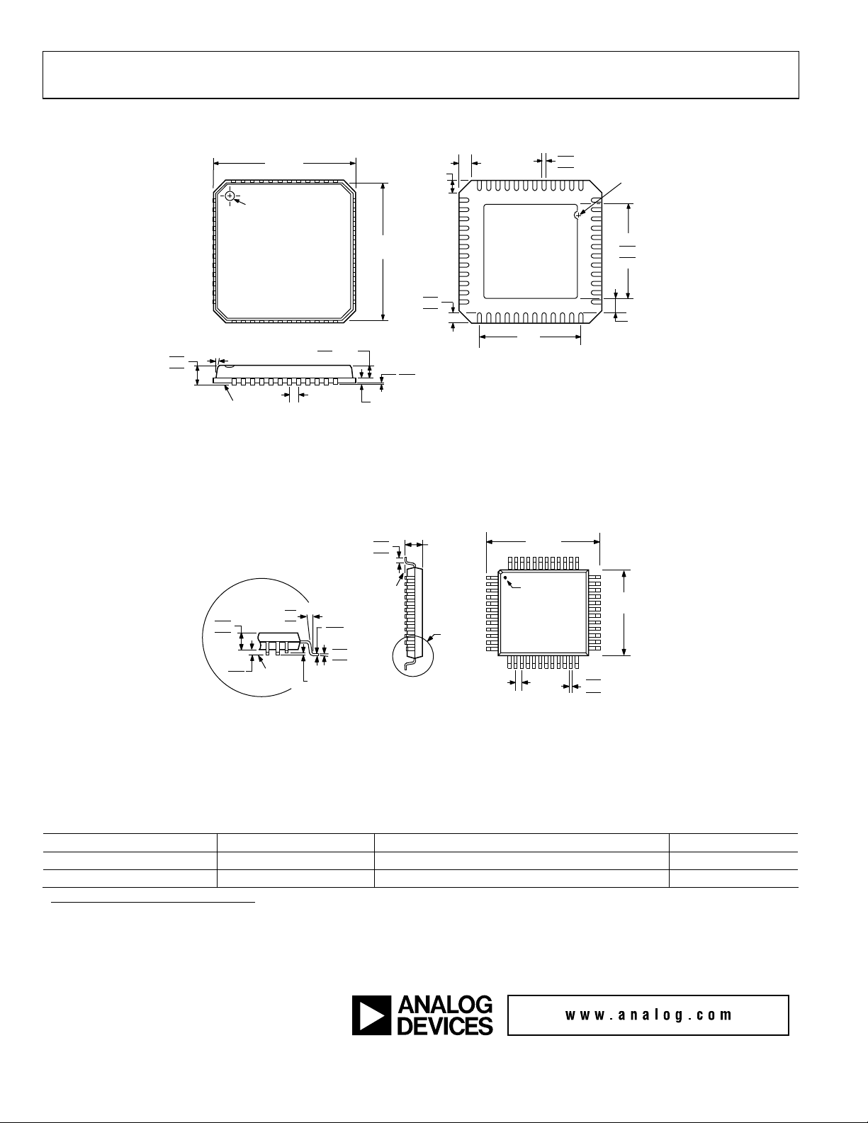
OUTLINE DIMENSIONS
0.30
0.23
0.18
PIN 1
48
INDICATOR
1
BSC SQ
PIN 1
INDICATOR
7.00
0.60 MAX
37
36
0.60 MAX
1.00
0.85
0.80
12° MAX
SEATING
PLANE
1.45
1.40
1.35
0.15
0.05
VIEW A
ROTATED 90° CCW
TOP
VIEW
0.80 MAX
0.65 TYP
0.50 BSC
COMPLIANT TO JEDEC STANDARDS MO-220-VKKD-2
6.75
BSC SQ
0.20REF
0.50
0.40
0.30
0.05 MAX
0.02 NOM
25
24
COPLANARITY
0.08
Figure 26. 48-Lead Lead Frame Chip Scale Package [LFCSP]
7 mm × 7 mm Body
(CP-48)
Dimensions shown in millimeters
10°
SEATING
PLANE
0.75
0.60
0.45
SEATING
PLANE
6°
0.20
2°
0.09
7°
3.5°
0°
0.08 MAX
COPLANARITY
COMPLIANT TO JEDEC STANDARDS MS-026BBC
1.60
MAX
VIEW A
Figure 27. 48-Lead Low Profile Quad Flat Package [LQFP]
(ST-48)
Dimensions shown in millimeters
EXPOSED
PAD
(BOTTOM VIEW)
5.50
REF
BSC SQ
48
1
PIN 1
TOP VIEW
(PINS DOWN)
12
13
0.50
BSC
9.00
5.25
5.10 SQ
4.95
12
13
0.25 MIN
37
36
7.00
BSC SQ
25
24
0.27
0.22
0.17
ORDERING GUIDE
1
Model
ADD8708WCPZ-REEL7
2
ADD8708WSTZ-REEL2 –40°C to +105°C 48-Lead Low Profile Quad Flat Package ST-48
1
Available in reels only.
2
Z = Pb-free part.
© 2004 Analog Devices, Inc. All rights reserved. Trademarks and
registered trademarks are the property of their respective owners.
D04614–0–10/04(0)
Temperature Range Package Description Package Option
–40°C to +105°C 48-Lead Lead Frame Chip Scale Package CP-48
Rev. 0 | Page 16 of 16
 Loading...