

12-Channel Gamma Buffers
FEATURES
Programmable 12-Channel Gamma Reference Generator
Mask Programmable Adjustable V
Upper/Lower Outputs Swing to V
COM
/GND
DD
Buffer
Continuous Output Current: 10 mA
V
Peak Output Current: 250 mA
COM
Outputs with Fast Settling Time for Load Change
Output Pins Are Compatible with ADD8701
Single-Supply Operation: 7 V to 16 V
Supply Current: 15 mA Max
APPLICATIONS
TFT LCD Panels
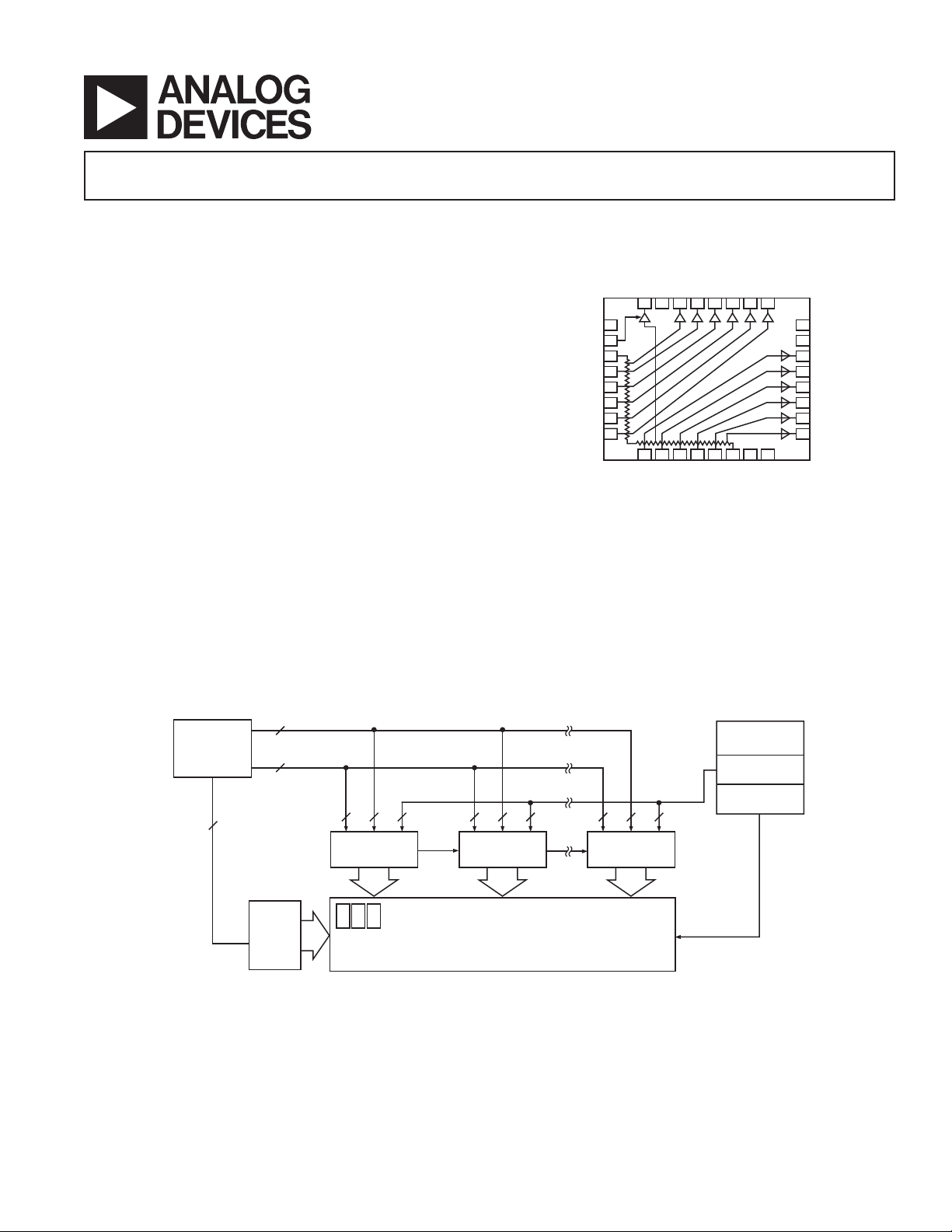
GENERAL DESCRIPTION
The ADD8702 is a low cost, mask programmable, 12-channel
gamma reference generator, plus an adjustable V
driver. This
COM
part is designed to provide gamma correction for high resolution
TFT LCD panels. The 12 gamma reference levels and V
COM
are
mask programmable to 0.3% resolution using the on-chip 500
chain resistor string. This reduces component and board costs.
The ADD8702 provides a complete programmed set of gamma
voltage references for the LCD source drivers. These references
settle quickly to load change. The V
output is stable with
COM
high capacitive loads and can source or sink 250 mA peak current. The V
output level can be adjusted using an external
COM
trim-potentiometer or discrete resistors.
with V
Buffer
COM
ADD8702
FUNCTIONAL BLOCK DIAGRAM
OUT
COM
V
GND
VGMA12
VGMA11
VGMA10
VGMA9
VGMA8
LOW
V
DD
V
VGMA7
GND
24
23
22
21
20
19
18
17
GND
V
DD
VGMA6
VGMA5
VGMA4
VGMA3
VGMA2
VGMA1
32 31 30 26 28 27 26 25
V
1
DD
V
ADJ
V
HIGH
VIN11
V
IN
V
V
V
2
3
4
10
5
6
9
IN
7
8
IN
7
8
IN
9 10 11 12 13 14 15 16
6
5
4
3
IN
IN
V
V
2
IN
IN
IN
V
V
V
COM
The output pins are compatible with the ADD8701. This allows
for single board design and fast turns for prototyping using the
initial ADD8701 board design.
The ADD8702 is specified over the temperature range of –40°C
to +85°C and comes in the 32-lead lead frame chip scale package (LFCSP) for compact board space.
PAN E L
TIMING
CONTROLLER
TIMING AND CONTROL
SCAN DRIVER CONTROL
SCAN
DRIVERS
768
SOURCE DRIVER
NO. 1
384
R
G B
Figure 1. Typical SVGA TFT LCD Application
REV. 0
Information furnished by Analog Devices is believed to be accurate and
reliable. However, no responsibility is assumed by Analog Devices for its
use, nor for any infringements of patents or other rights of third parties that
may result from its use. No license is granted by implication or otherwise
under any patent or patent rights of Analog Devices. Trademarks and
registered trademarks are the property of their respective companies.
ADD8702
SOURCE DRIVER
NO. 2
384
TFT COLOR PANEL
1024 768
GAMMA
REFERENCE
VOLTAG ES
SOURCE DRIVER
NO. 8
384
GAMMA
V
COM
One Technology Way, P.O. Box 9106, Norwood, MA 02062-9106, U.S.A.
Tel: 781/329-4700 www.analog.com
Fax: 781/326-8703 © 2003 Analog Devices, Inc. All rights reserved.

ADD8702–SPECIFICATIONS
ELECTRICAL CHARACTERISTICS
(VDD = 16 V, TA = 25ⴗC, unless otherwise specified.)
Parameter Symbol Conditions Min Typ Max Unit
OUTPUT ACCURACY
V
ERROR V
SYSTEM
SY ERROR
10 50 mV
MASK PROGRAMMABLE
RESISTOR STRING
Total Resistor String R
Resistor Matching R
TOTAL
MATCH
500 Elements V
LOW
to V
HIGH
22.5 kΩ
Any Two Segments 1 %
OUTPUT CHARACTERISTICS
Output Voltage High V
OUT
(VGMA11, VGMA12) I
Output Voltage Mid V
OUT
IL = 100 µA 15.995 V
= 5 mA 15.85 15.95 V
L
–40°C ≤ T
≤ +85°C 15.75 V
A
IL = 5 mA 14.6 V
(VGMA3 to VGMA10)
Output Voltage Low V
OUT
IL = 100 µA5mV
(VGMA1, VGMA2) IL = 5 mA 50 150 mV
Continuous Output Current I
Peak Output Current I
Settling Time—Voltage t
CHARACTERISTICS
V
COM
Continuous Output Current I
Peak Output Current I
Settling Time—Voltage t
OUT
PK
S
OUT
PK
S
–40°C ≤ T
1 V Step 0.1%, RL = 10 kΩ, CL = 200 pF 1 µs
1 V Step 0.1%, RL = 10 kΩ, CL = 200 pF 0.8 µs
≤ +85°C 250 mV
A
10 mA
150 mA
35 mA
250 mA
SUPPLY CHARACTERISTICS
Supply Voltage V
DD
716V
Power Supply Rejection Ratio PSRR VS = 6 V to 17 V, –40°C ≤ TA ≤ +85°C6875 dB
SUPPLY CURRENT I
SYS
No Load 11 15 mA
–40°C ≤ TA ≤ +85°C16mA
Specifications subject to change without notice.
REV. 0–2–
ADD8702
ABSOLUTE MAXIMUM RATINGS*
Supply Voltage (VS) . . . . . . . . . . . . . . . . . . . . . . . . . . . . . . 18 V
Storage Temperature Range . . . . . . . . . . . . . –65°C to +150°C
Operating Temperature Range . . . . . . . . . . . .–40°C to +85°C
Junction Temperature Range . . . . . . . . . . . . . –65°C to +150°C
Lead Temperature Range (Soldering, 60 sec.) . . . . . . . . 300°C
ESD Tolerance (HBM) . . . . . . . . . . . . . . . . . . . . . . . ± 1,000 V
*Stresses above those listed under Absolute Maximum Ratings may cause perma-
nent damage to the device. This is a stress rating only; functional operation of the
device at these or any other conditions above those indicated in the operational
sections of this specification is not implied. Exposure to absolute maximum rating
conditions for extended periods may affect device reliability.
ORDERING GUIDE
Temperature Package Package
Model Range Description Option
ADD8702ACP-R2 –40°C to +85°C 32-Lead LFCSP CP-32
ADD8702ACP-REEL –40°C to +85°C 32-Lead LFCSP CP-32
ADD8702ACP-REEL7 –40°C to +85°C 32-Lead LFCSP CP-32
PIN CONFIGURATION
OUT
COM
32 V
31 GND
30 VGMA12
29 VGMA11
Package Type
1
JA
2
JB
Unit
32-Lead LFCSP (CP) 35 13 °C/W
NOTES
1
θJA is specified for worst-case conditions, i.e., θ
in circuit board for surface-mount packages.
2
ψJB is applied for calculating the junction temperature by reference to the board
temperature.
28 VGMA10
27 VGMA9
26 VGMA8
25 VGMA7
is specified for device soldered
JA
V
1
DD
ADJ 2
V
COM
V
HIGH
VIN11 4
V
10 5
IN
9 6
V
IN
V
8 7
IN
7 8
V
IN
PIN 1
INDICATOR
3
ADD8702
TOP VIEW
6 9
5 10
4 11
3 12
2 13
IN
IN
IN
IN
V
IN
V
V
V
V
14
LOW
V
15
V
DD
24 GND
23 V
22 VGMA6
21 VGMA5
20 VGMA4
19 VGMA3
18 VGMA2
17 VGMA1
GND 16
DD
PIN FUNCTION DESCRIPTIONS
Pin No. Mnemonic Description
1, 15, 23 V
2V
3V
4–13 V
14 V
DD
ADJ V
COM
HIGH
11–VIN2Gamma Buffer Inputs
IN
LOW
Power (+)
Adjust Input
COM
Highest Gamma Input Voltage
Lowest Gamma Input Voltage
16, 24, 31 GND Power (–)
17–22, 25–30 VGMA1–VGMA12 Gamma Buffer Outputs
32 V
OUT V
COM
Buffer Output
COM
CAUTION
ESD (electrostatic discharge) sensitive device. Electrostatic charges as high as 4000 V readily
accumulate on the human body and test equipment and can discharge without detection. Although the
ADD8702 features proprietary ESD protection circuitry, permanent damage may occur on devices
subjected to high energy electrostatic discharges. Therefore, proper ESD precautions are recommended
to avoid performance degradation or loss of functionality.
REV. 0
–3–

ADD8702–Typical Performance Characteristics
)
)
CAPACITIVE LOAD (pF)
PHASE SHIFT (Degrees)
180
40
0 200 1,200400 600 800 1,000
160
140
120
80
60
100
VDD = 16V
GAMMA 1 TO 12
R
L
= 2k
GAMMA 12
GAMMA 1
12
TA = 25C
10
8
6
4
SUPPLY CURRENT (mA)
2
0
04 16
SUPPLY VOLTAGE (V)
812
TPC 1. Supply Current vs.
Supply Voltage
10
VDD = 16V
0
–10
GAIN (dB)
–20
–30
–40
GAMMA 10 TO 12
1M 10M
FREQUENCY (Hz)
2k, 10k
150
TPC 4. Frequency Response
vs. Resistive Loading
12
V
= 16V
DD
11
10
9
8
7
SUPPLY CURRENT (mA)
6
5
–40 85
25
TEMPERATURE (C)
TPC 2. Supply Current vs.
Temperature
10
VDD = 16V
V
COM
0
–10
–20
GAIN (dB)
–30
–40
30M100k
–50
1M 10M
FREQUENCY (Hz)
2k, 10k
150
30M100k
TPC 5. Frequency Response
vs. Resistive Loading
10
VDD = 16V
GAMMA 1 TO 9
0
–10
GAIN (dB)
–20
–30
–40
100k 30M
FREQUENCY (Hz)
2k, 10k
150
1M 10M
TPC 3. Frequency Response
vs. Resistive Loading
20
VDD = 16V
GAMMA 1 TO 9
10
0
GAIN (dB)
–10
–20
–30
340pF
540pF
1040pF
1M 10M
FREQUENCY (Hz
TPC 6. Frequency Response
vs. Capacitive Loading
50pF
100pF
30M100k
20
VDD = 16V
GAMMA 10 TO 12
10
0
GAIN (dB)
–10
–20
–30
TPC 7. Frequency Response
vs. Capacitive Loading
340pF
540pF
1040pF
1M 10M
FREQUENCY (Hz
50pF
100pF
20
VDD = 16V
V
COM
10
0
GAIN (dB)
–10
–20
30M100k
–30
TPC 8. Frequency Response
vs. Capacitive Loading
340pF
540pF
1040pF
1M 10M
FREQUENCY (Hz)
100pF
50pF
30M100k
TPC 9. Input and Output Phase
Shift vs. Capacitive Load
REV. 0–4–

ADD8702
V
= 16V
DD
= 10k
R
L
C
= 100pF
L
VOLTA GE (2V/DIV)
TIME (2s/DIV)
TPC 10. Large Signal Transient
Response
11
10
9
8
7
6
5
4
AMPLITUDE (V)
3
2
1
0
–200 1,800
120pF
320pF
520pF
200 600 1,000 1,400
TIME (ns)
VDD = 16V
GAMMA = 2
1F
TPC 13. Transient Load
Response vs. Capacitive Load
10F
16
VDD = 16V
= 33
R
14
NULL
= 100pF
C
L
12
10
8
6
SLEW RATE (V/s)
4
2
0
–40 85
V
SLEW RATE FALLING
COM
V
SLEW RATE RISING
COM
25
TEMPERATURE (C)
TPC 11. Slew Rate vs. Temperature
11
10
9
8
320pF
7
6
5
4
AMPLITUDE (V)
3
2
1
0
–200 1,800
120pF
520pF
200 600 1,000 1,400
TIME (ns)
VDD = 16V
GAMMA = 11
10F
1F
TPC 14. Transient Load
Response vs. Capacitive Load
VOLTA GE (20mV/DIV)
7V < VDD < 16V
= 33
R
NULL
= 0.1F
C
L
TIME (20s/DIV)
TPC 12. Small Signal Transient
Response
11
10
9
8
120pF
7
6
5
4
AMPLITUDE (V)
3
2
1
0
–200 1,800
320pF
520pF
200 600 1,000 1,400
TIME (ns)
VDD = 16V
V
1F10F
TPC 15. Transient Load
Response vs. Capacitive Load
COM
100
VDD = 16V
90
GAMMA 1 TO 9
80
70
60
50
40
30
20
OUTPUT VOLTAGE ERROR (mV)
10
0
0.001 0.01 1000.1 1 10
LOAD CURRENT (mA)
SOURCE
TPC 16. Output Voltage
Error vs. Load Current
SINK
1,400
VDD = 16V
GAMMA 10 TO 12
1,200
1,000
800
600
400
OUTPUT VOLTAGE ERROR (mV)
200
0
0.001 0.01 1000.1 1 10
LOAD CURRENT (mA)
TPC 17. Output Voltage
Error vs. Load Current
SINK
SOURCE
50
VDD = 16V
45
V
COM
40
35
30
25
20
15
10
OUTPUT VOLTAGE ERROR (mV)
5
0
0.001 0.01 1000.1 1 10
LOAD CURRENT (mA)
TPC 18. Output Voltage
Error vs. Load Current
SOURCE
SINK
REV. 0
–5–

ADD8702
)
)
6,000
VDD = 16V
= 25C
T
A
5,000
ALL CHANNELS
4,000
3,000
2,000
1,000
FREQUENCY (No. of Amplifiers)
0
–14 –6 2 10 182634
–22
OUTPUT VOLTAGE ERROR (mV)
TPC 19. Output Voltage Error
Distribution
70
VDD = 16V
60
50
40
30
20
10
VOLTA G E NOISE DENSITY (nV/ Hz)
–10
AND BUFFERS 1 TO 9
V
COM
MARKER SET @ 10kHz
MARKER READING = 25.7nV/ Hz
0
051015 20 25
FREQUENCY (Hz
TPC 22. Voltage Noise Density
vs. Frequency
80
ALL CHANNELS
= 8V
V
60
DD
= 25C
T
A
40
20
0
–20
–40
–60
–80
–100
POWER SUPPLY REJECTION RATIO (dB)
–120
100 1k 10M10k 100k 1M
FREQUENCY (Hz)
PSRR
TPC 20. Power Supply Rejection
Ratio vs. Frequency
70
VDD = 16V
60
BUFFERS 10 TO 12
MARKER SET @ 10kHz
MARKER READING = 36.6nV/ Hz
50
40
30
20
10
0
VOLTA G E NOISE DENSITY (nV/ Hz)
–10
051015 20 25
FREQUENCY (Hz
TPC 23. Voltage Noise Density
vs. Frequency
VOLTA GE (3V/DIV)
TIME (40s/DIV)
TPC 21. No Phase Reversal
REV. 0–6–

APPLICATIONS
Figure 1 is a block diagram of the configuration of an XGAcompatible (1024 ⫻ 768) TFT color panel with the ADD8702
providing gamma correction reference voltages to the source
drivers and an integrated V
16V
driver for LCD common node.
COM
BUFFER
R
NULL
V
HIGH
VIN11
V
IN
ADD8702
A12
A11
10
A10
GMA 12
GMA 11
GMA 10
C
R
T
L
Figure 2. Bandwidth Measurement Information
Panel size and resolution determine the number of gamma
reference voltages required. For a 256-grayscale level, 8-bit color
scheme, 6 ⫻ 2 external reference nodes should be sufficient to
match the characteristics of the LCD driver to the characteristics
of the actual LCD panel for improved picture quality. External
reference gamma correction voltages are often generated using
a simple resistor ladder. Using the ADD8702, the resistor
ladder is incorporated in the IC for reduced cost and number
of components.
16V
5V
BUFFER
33 1k
V
TH
0.1s
V
TH
10V
5V
0V
Figure 3. Transient Load Regulation Test Circuit
The ADD8702 is designed to meet the rail-to-rail capability
needed by the application, yet offers the lowest cost per channel
solution. The ADD8702 gamma buffers offer 10 mA continuous
drive current capability. To be more competitive, the design
maximizes the die area by allowing specific channels to swing to
the positive rail and negative rail. So it is imperative that the
channels swinging close to the supply rail be used for the positive gamma references and the channels swinging close to GND
be used for the negative gamma references. The V
buffer can
COM
handle up to 35 mA continuous output current and can drive up
to 1,000 pF pure capacitive load. Provision is available to adjust
the V
voltage to a desired level. Refer to Figure 4 for an
COM
example of an application circuit for adjusting the output of the
buffer.
V
COM
GMA 9
GMA 8
GMA 7
GMA 6
GMA 5
GMA 4
GMA 3
GMA 2
GMA 1
V
COM
V
IN
V
IN
V
IN
V
IN
VIN5
V
IN
V
IN
V
IN
V
LOW
V
DD
GND
ADJUST
V
2k
COM
A9
A8
A7
A6
A5
A4
A3
A2
A1
AMP
LCD SOURCE DRIVER
LCD COMMON PLANE
9
8
7
6
4
3
2
32k
ADD8702
Figure 4. Application Circuit
Table I. ADD8702 – 000 Mask Option, Resistor Tap Points
(0 ≤ ≤ 500) VDD = 12.5 V, V
= 12.5 V, and V
HIGH
LOW
= GND
POSITIVE GAMMA REFERENCES
NEGATIVE GAMMA REFERENCES
REV. 0
Tap Point () Voltage Unit
VGMA1 8 0.2 V
VGMA2 57 1.43 V
VGMA3 84 2.11 V
VGMA4 115 2.89 V
VGMA5 139 3.48 V
VGMA6 194 4.86 V
VGMA7 218 5.45 V
VGMA8 298 7.45 V
VGMA9 371 9.29 V
VGMA10 418 10.45 V
VGMA11 442 11.04 V
VGMA12 488 12.2 V
V
COM
200 5 V
–7–

ADD8702
OUTLINE DIMENSIONS
32-Lead Lead Frame Chip Scale Package [LFCSP]
(CP-32)
Dimensions shown in millimeters
PIN 1
INDICATOR
1.00
0.90
0.80
12 MAX
SEATING
PLANE
5.00
BSC SQ
TOP
VIEW
0.80 MAX
0.65 NOM
0.30
0.23
0.18
COMPLIANT TO JEDEC STANDARDS MO-220-VHHD-2
4.75
BSC SQ
0.20 REF
0.05 MAX
0.02 NOM
0.60 MAX
0.50
BSC
0.50
0.40
0.30
COPLANARITY
0.08
0.60 MAX
25
24
17
16
BOTTOM
VIEW
3.50
REF
PIN 1
32
9
INDICATOR
1
3.25
3.10
SQ
2.95
8
C03820–0–6/03(0)
–8–
REV. 0
 Loading...