

12-Channel Gamma Buffers
with VCOM Buffer
ADD8701
FEATURES
Single-Supply Operation: 7 V to 16 V
Dual-Supply Operation: 3.5 V to 8 V
Supply Current: 13 mA Max
Upper/Lower Buffers Swing to V
/GND
DD
Continuous Output Current: 10 mA
VCOM Peak Output Current: 250 mA
Offset Voltage: 15 mV Max
Slew Rate: 6 V/s
Fast Settling Time with Large C-Load
APPLICATIONS
TFT LCD Panels
GENERAL DESCRIPTION
The ADD8701 is a low cost, 12-channel buffer amplifier and
VCOM driver that operates from a single supply. The part is
designed for high resolution TFT LCD panels, and is built on
an advanced, high voltage, CBCMOS process.
The buffers have high slew rate, 10 mA continuous output current,
and high capacitive load drive capability. The VCOM buffer has
increased drive of 35 mA and can drive large capacitive loads. The
ADD8701 offers wide supply range and offset voltages below 15 mV.
FUNCTIONAL BLOCK DIAGRAM
OUT
VCOM
GND
V12
V11
V
VCOM IN
IN12
IN11
IN10
IN9
IN8
IN7
32
31
1
DD
2
3
4
5
6
7
8
9
10
IN6
IN5
V10V9V8
30
26
28
11
12
13
IN4
IN3
IN2
V7
27
26
25
24
GND
V
23
DD
22
V6
21
V5
V4
20
19
V3
18
V2
V1
17
14
15
16
DD
IN1
V
GND
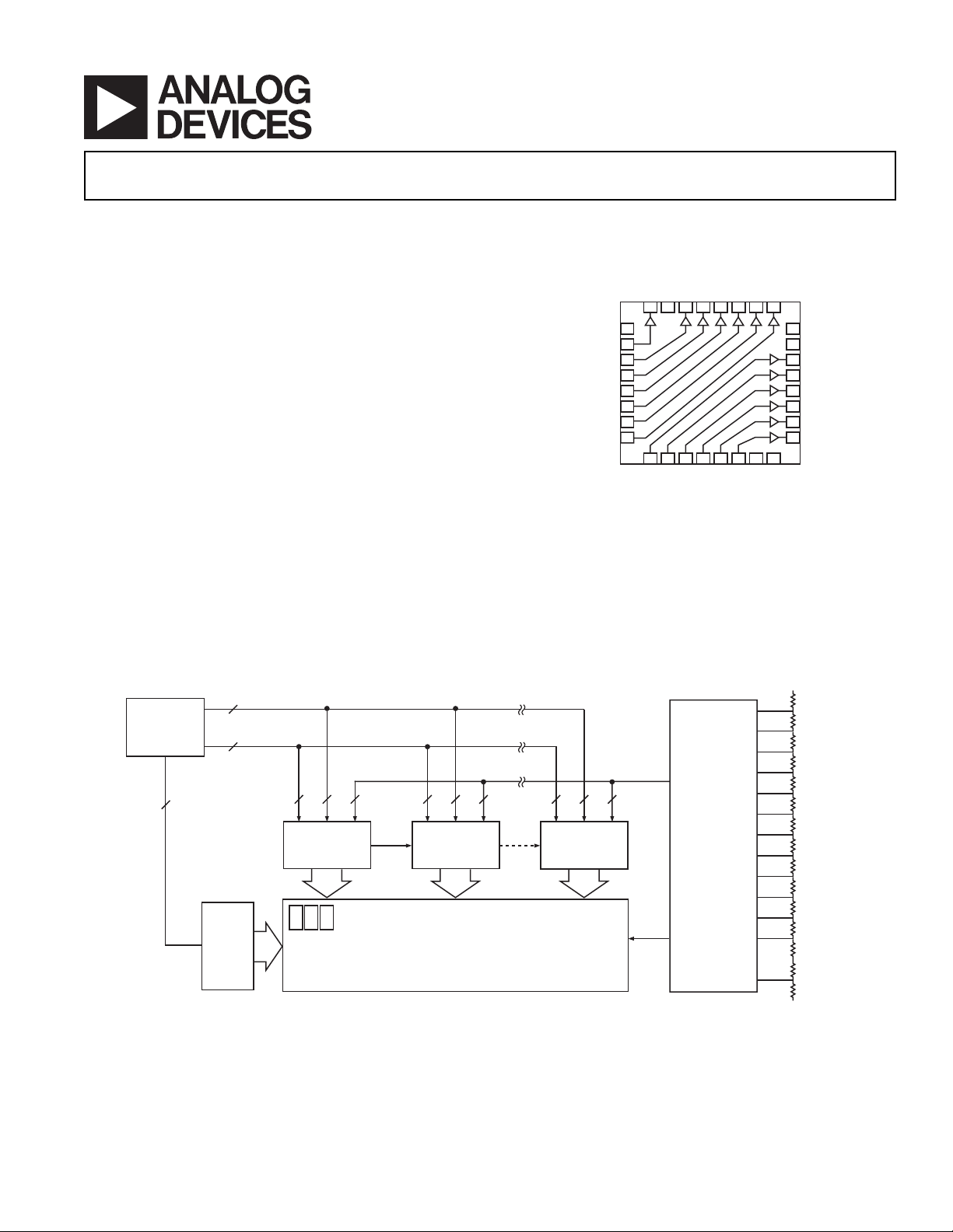
The ADD8701 is specified over the –40ºC to +85ºC temperature range and is available in a 32-lead lead frame chip scale
package (LFCSP).
All inputs and outputs incorporate internal ESD protection
circuits.
PAN E L
TIMING
CONTROLLER
TIMING AND CONTROL
SCAN DRIVER CONTROL
SCAN
DRIVERS
768
SOURCE DRIVER
NO. 1
384
R
G
B
SOURCE DRIVER
NO. 2
384
TFT COLOR PANEL
1024 ⴛ 768
Figure 1. Typical SVGA TFT-LCD Application
REV. 0
Information furnished by Analog Devices is believed to be accurate and
reliable. However, no responsibility is assumed by Analog Devices for its
use, nor for any infringements of patents or other rights of third parties that
may result from its use. No license is granted by implication or otherwise
under any patent or patent rights of Analog Devices. Trademarks and
registered trademarks are the property of their respective companies.
V
DD
V12
GAMMA
REFERENCE
VOLTAGES
RESISTOR
SOURCE DRIVER
NO. 8
384
ADD8701
VCOM OUT
V1
VCOM IN
LADDER
GND
V
DD
One Technology Way, P.O. Box 9106, Norwood, MA 02062-9106, U.S.A.
Tel: 781/329-4700 www.analog.com
Fax: 781/326-8703 © 2003 Analog Devices, Inc. All rights reserved.

ADD8701–SPECIFICATIONS
ELECTRICAL CHARACTERISTICS
(7 V ≤ VDD ≤ 16 V, TA = 25°C, unless otherwise specified.)
Parameter Symbol Condition Min Typ Max Unit
INPUT CHARACTERISTICS
Offset Voltage V
OS
415 mV
Offset Voltage Drift ∆VOS/∆T –40°C ≤ TA ≤ +85°C 5 µV/°C
Input Bias Current I
B
–40°C ≤ T
≤ +85°C 1.5 µA
A
Input Voltage Range –0.5 V
Input Impedance Z
Input Capacitance C
IN
IN
0.5 1.1 µA
+ 0.5 V
DD
400 kΩ
1pF
OUTPUT CHARACTERISTICS
Output Voltage High (V11, V12) V
Output Swing (V3 to V10) V
Output Swing (V3 to V10) V
Output Voltage Low (V1, V2) V
Continuous Output Current I
Peak Output Current I
OUT
OUT
OUT
OUT
OUT
PK
IL = 100 µA 15.995 V
= 16 V, IL = 5 mA 15.85 15.9 V
V
DD
–40°C ≤ T
V
DD
–40°C ≤ T
≤ +85°C 15.75 V
A
= 7 V, IL = 5 mA 6.75 6.85 V
≤ +85°C 6.65 V
A
IL = 5 mA, VDD = 16 V 14.6 V
IL = 5 mA, VDD = 7 V 5.6 V
IL = 100 µA 5 mV
= 16 V, IL = 5 mA 85 150 mV
V
DD
–40°C ≤ T
V
DD
–40°C ≤ T
≤ +85°C 250 mV
A
= 7 V, IL = 5 mA 140 300 mV
≤ +85°C 400 mV
A
10 mA
VDD = 16 V 150 mA
VCOM CHARACTERISTICS
Continuous Output Current I
Peak Output Current I
OUT
PK
VDD = 16 V 250 mA
35 mA
TRANSFER CHARACTERISTICS
Gain A
VCL
Gain Linearity NL R
RL = 2 kΩ 0.995 0.9985 1.005 V/V
–40°C ≤ T
= 10 kΩ
L
VO = 0.5 to (V
≤ +85°C 0.995 0.9980 1.005 V/V
A
– 0.5 V) 0.01 %
DD
SUPPLY CHARACTERISTICS
Supply Voltage V
DD
Power Supply Rejection Ratio PSRR V
Supply Current I
SYS
= 6 V to 17 V
DD
–40°C ≤ T
≤ +85°C 70 90 dB
A
No Load 10 13 mA
716V
–40°C ≤ TA ≤ +85°C 15 mA
DYNAMIC PERFORMANCE
Slew Rate SR RL = 10 kΩ, CL = 200 pF 4 6 V/µs
Bandwidth BW –3 dB, R
Settling Time to 0.1% (Buffers) t
Settling Time to 0.1% (VCOM) t
S
S
Phase Margin fo R
1 V, RL = 10 kΩ, CL = 200 pF 1.1 µs
1 V, RL = 10 kΩ, CL = 200 pF 0.7 µs
L
= 10 kΩ, CL = 200 pF 4.5 MHz
L
= 10 kΩ, CL = 200 pF 55 Degrees
Channel Separation 75 dB
NOISE PERFORMANCE
Voltage Noise Density e
Current Noise Density i
Specifications subject to change without notice.
n
e
n
n
f = 1 kHz 26 nV/√Hz
f = 10 kHz 25 nV/√Hz
f = 10 kHz 0.8 pA/√Hz
REV. 0–2–
ADD8701
ABSOLUTE MAXIMUM RATINGS*
Supply Voltage (VDD) . . . . . . . . . . . . . . . . . . . . . . . . . . . . 18 V
Input Voltage . . . . . . . . . . . . . . . . . . . . . –0.5 V to V
+ 0.5 V
DD
Storage Temperature Range . . . . . . . . . . . . . –65°C to +150°C
Operating Temperature Range . . . . . . . . . . . . –40°C to +85°C
Junction Temperature Range . . . . . . . . . . . . . –65°C to +150°C
Lead Temperature Range (Soldering, 60 sec) . . . . . . . . 300°C
ESD Tolerance (HBM) . . . . . . . . . . . . . . . . . . . . . . . ±1,000 V
*Stresses above those listed under Absolute Maximum Ratings may cause perma-
nent damage to the device. This is a stress rating only; functional operation of the
device at these or any other conditions above those indicated in the operational
sections of this specification is not implied. Exposure to absolute maximum rating
conditions for extended periods may affect device reliability.
Package Type
1
JA
2
JB
Unit
32-Lead LFCSP (CP) 35 13 °C/W
NOTES
1
θJA is specified for worst-case conditions, i.e., θ
in circuit board for surface-mount packages.
2
ψJB is applied for calculating the junction temperature by reference to the board
is specified for device soldered
JA
temperature.
ORDERING GUIDE
Model Temperature Package Package
Range Description Option
ADD8701ACP –40°C to +85°C 32-Lead LFCSP CP-32
PIN CONFIGURATION
32 VCOM OUT
31 GND
30 V12
29 V11
28 V10
27 V9
26 V8
25 V7
V
DD
VCOM IN 2
IN12 3
IN11 4
IN10 5
IN9 6
IN8 7
IN7 8
1
PIN 1
INDICATOR
ADD8701
TOP VIEW
IN6 9
IN5 10
IN4 11
IN3 12
IN2 13
24 GND
23 V
DD
22 V6
21 V5
20 V4
19 V3
18 V2
17 V1
15
DD
IN1 14
V
GND 16
PIN FUNCTION DESCRIPTION
Pin No. Mnemonic Description
1, 15, 23 V
DD
Power (+)
2 VCOM IN VCOM Buffer Input
3–14 IN12–IN1 Gamma Buffer Inputs
16, 24, 31 GND Power (–)
17–22, 25–30 V1–V12 Gamma Buffer Outputs
32 VCOM OUT VCOM Buffer Output
CAUTION
ESD (electrostatic discharge) sensitive device. Electrostatic charges as high as 4000 V readily
accumulate on the human body and test equipment and can discharge without detection. Although the
ADD8701 features proprietary ESD protection circuitry, permanent damage may occur on devices
subjected to high energy electrostatic discharges. Therefore, proper ESD precautions are recommended
to avoid performance degradation or loss of functionality.
REV. 0
–3–

ADD8701–Typical Performance Characteristics
1,400
TA = 25C
< 16V
7V < V
1,200
1,000
800
600
400
NUMBER OF AMPLIFIERS
200
DD
0
–5 –3 –1 1 3 5
–7 9
INPUT OFFSET VOLTAGE – mV
7
TPC 1. Input Offset Voltage Distribution
8
VDD = 8V
6
BUFFERS 10 TO 12
4
2
0
–2
–4
OFFSET VOLTAGE – mV
–6
–8
–10
–8 –6 8
–4 –2 0 4 62
COMMON-MODE VOLTAGE – V
TPC 4. Offset Voltage vs.
Common-Mode Voltage
7,000
6,000
5,000
4,000
3,000
2,000
NUMBER OF AMPLIFIERS
1,000
0
TCVOS – V/C
7V < VDD < 16V
TPC 2. TCVOS Distribution
8
VDD = 8V
6
VCOM, BUFFERS 1 TO 9
4
2
0
–2
–4
OFFSET VOLTAGE – mV
–6
–8
–10
–8 –6 8
–4 –2 0 4 62
COMMON-MODE VOLTAGE – V
TPC 5. Offset Voltage vs.
Common-Mode Voltage
20
7V < VDD < 16V
15
10
5
0
–5
–10
INPUT OFFSET VOLTAGE – mV
–15
–20
405101520253035
–40 85
VCOM
25
TEMPERATURE – C
BUFFER 1
BUFFER 12
TPC 3. Input Offset Voltage
vs. Temperature
0
VCOM AND BUFFERS 1 TO 9
–100
–200
–300
–400
–500
–600
–700
INPUT BIAS CURRENT – nA
–800
–900
–40 85
TEMPERATURE – C
VDD = 16V
VDD = 7V
25
TPC 6. Input Bias Current vs.
Temperature
350
BUFFERS 10 TO 12
300
250
200
150
100
INPUT BIAS CURRENT – nA
50
0
–40 85
TEMPERATURE – C
V
= 7V
DD
= 16V
V
DD
25
TPC 7. Input Bias Current vs.
Temperature
100
VDD = 16V
BUFFERS 1, 2
10
1
0.1
∆OUTPUT VOLTAGE – V
0.01
0.001
0.01 0.1 100110
LOAD CURRENT – mA
SOURCE
TPC 8. Output Voltage to
Supply Rail vs. Load Current
SINK
100
VDD = 16V
BUFFERS 3 TO 9
10
1
0.1
∆OUTPUT VOLTAGE – V
0.01
0.001
0.01 0.1 100110
SOURCE
LOAD CURRENT – mA
TPC 9. Output Voltage to
Supply Rail vs. Load Current
SINK
REV. 0–4–

ADD8701
100
V
= 16V
DD
BUFFER 10
10
1
0.1
∆OUTPUT VOLTAGE – V
0.01
0.001
0.01 0.1 100110
SINK
LOAD CURRENT – mA
TPC 10. Output Voltage to
Supply Rail vs. Load Current
12
VCM = 1/2 V
10
8
6
4
SUPPLY CURRENT – mA
2
DD
SOURCE
100
VDD = 16V
BUFFERS 11, 12
10
1
0.1
∆OUTPUT VOLTAGE – V
0.01
0.001
0.01 0.1 100110
SINK
LOAD CURRENT – mA
TPC 11. Output Voltage to
Supply Rail vs. Load Current
12
10
8
6
4
SUPPLY CURRENT – mA
2
SOURCE
V
= 16V
DD
VDD = 7V
10
VDD = 16V
VCOM
1
0.1
0.01
∆OUTPUT VOLTAGE – V
0.001
0.0001
0.01 0.1 100110
LOAD CURRENT – mA
SOURCE
SINK
TPC 12. Output Voltage to
Supply Rail vs. Load Current
20
VDD = 16V
VCOM AND BUFFERS 1 TO 9
10
0
–10
GAIN – dB
150
–20
10k
2k
1k
560
0
04 16
812
SUPPLY VOLTAGE – V
TPC 13. Supply Current vs.
Supply Voltage
20
VDD = 16V
BUFFERS 10 TO 12
10
150
10M
10k
2k
1k
560
0
–10
GAIN – dB
–20
–30
100k
1M 30M
FREQUENCY – Hz
TPC 16. Frequency Response
vs. Resistive Loading
0
–40 85
25
TEMPERATURE – C
TPC 14. Supply Current vs.
Temperature
80
ALL CHANNELS
V
= 8V
60
DD
T
= +25C
A
40
20
0
–20
–40
–60
–80
–100
POWER SUPPLY REJECTION RATIO – dB
–120
100 1k 10M10k 100k 1M
FREQUENCY – Hz
PSRR
TPC 17. Power Supply Rejection
Ratio vs. Frequency
–30
100k
1M 30M
FREQUENCY – Hz
TPC 15. Frequency Response
vs. Resistive Loading
20
VDD = 16V
VCOM, BUFFERS 1 TO 9
10
0
–10
–20
GAIN – dB
–30
–40
–50
100k
540pF
1040pF
1M 30M
FREQUENCY – Hz
TPC 18. Frequency Response
vs. Capacitive Loading
10M
100pF
50pF
10M
REV. 0
–5–

ADD8701
20
VDD = 16V
BUFFERS 10 TO 12
10
0
–10
–20
GAIN – dB
–30
–40
–50
100k
540pF
1040pF
1M 30M
FREQUENCY – Hz
TPC 19. Frequency Response
vs. Capacitive Loading
VDD = 16V
VOLTA GE – 2V/DIV
TIME – 2s/DIV
TPC 22. Large-Signal Transient
Response
10M
100pF
50pF
180
VDD = 7V
= 2k
R
L
160
140
120
100
80
PHASE SHIFT – Degrees
60
40
VCOM
0 200 1,200
CHANNELS 11 AND 12
CHANNELS 3 TO 9
CHANNELS 1 AND 2
400 600 800 1,000
CAPACITIVE LOAD – pF
TPC 20. Input-Output Phase
Shift vs. Capacitive Load
16
VDD = 16V
R
14
12
10
8
6
SLEW RATE – V/s
4
2
0
= 33
NULL
= 100pF
C
L
VCOM SLEW RATE FALLING
VCOM SLEW RATE RISING
–40 85
25
TEMPERATURE – C
TPC 23. Slew Rate vs. Temperature
180
VDD = 16V
= 2k
R
L
160
140
120
100
80
PHASE SHIFT – Degrees
60
40
0 200 1,200
VCOM
CAPACITIVE LOAD – pF
CHANNEL 11
CHANNEL 3
CHANNEL 1
400 600 800 1,000
TPC 21. Input-Output Phase
Shift vs. Capacitive Load
VOLTA GE – 20mV/DIV
7V < VDD < 16V
SERIES = 33
R
OUT
= 0.1F
C
LOAD
TIME – 20s/DIV
TPC 24. Small Signal Transient
Response
100
VDD = 8V
90
V
= 50mV
IN
= 2k
R
L
80
= 25C
T
A
70
60
50
40
OVERSHOOT – %
30
20
10
0
10 100 10k1k
CAPACITIVE LOAD – pF
–OS
+OS
TPC 25. Small-Signal Overshoot
vs. Capacitive Load
12
VCOM
V
= 8V
DD
= 5k
R
8
L
= 100pF
C
L
= 33
R
NULL
4
= 25C
T
A
0
STEP SIZE – V
–4
–8
–12
400 1,400
600 800 1,000 1,200
SETTLING TIME – ns
+tS (0.1%)
–tS (0.1%)
TPC 26. Settling Time vs. Step Size
VOLTA GE – 3V/DIV
TIME – 40s/DIV
TPC 27. No Phase Reversal
REV. 0–6–

ADD8701
70
VDD = 16V
60
VCOM AND BUFFERS 1 TO 9
MARKER SET @ 10kHz
MARKER READING = 25.7nV/ Hz
50
40
30
20
10
0
VOLTA G E NOISE DENSITY – nV/ Hz
–10
051015 20 25
FREQUENCY – Hz
TPC 28. Voltage Noise Density
vs. Frequency
70
VDD = 16V
60
BUFFERS 10 TO 12
MARKER SET @ 10kHz
MARKER READING = 36.6nV/ Hz
50
40
30
20
10
0
VOLTA G E NOISE DENSITY – nV/ Hz
–10
051015 20 25
FREQUENCY – Hz
TPC 29. Voltage Noise Density
vs. Frequency
APPLICATIONS
LCD Gamma Reference Buffers
In high resolution TFT-LCD displays, gamma correction must
be performed to correct the nonlinearity in the LCD panel’s
transmission characteristics. A typical TFT-LCD panel consisting
of 256 grayscale levels takes an 8-bit digital word to select an
appropriate gamma reference voltage. An 8-bit source driver may
use 12 analog voltages that match the characteristic gamma curve
for optimum panel picture quality. The ADD8701 is specifically
designed to generate analog reference voltages to meet the gamma
characteristics of an LCD panel used by the source driver. The
gamma reference buffers offer 10 mA drive capability.
The ADD8701 is designed to meet the rail-to-rail capability
needed by the application and yet offers a low cost-per-channel
solution. The design maximizes the die area by offering channels
to swing to the positive and negative rails. It is imperative that
the channels swinging close to the supply rail be used for the
positive gamma references and that the channels swinging close
to GND be used for the negative gamma references. See Figure 2
for an example of the application circuit.
LCD VCOM Buffer
The output of the VCOM buffer is designed to control the voltage
on the back plate of the LCD display. The buffer must be capable
of sinking and sourcing capacitive pulse current. The amplifier
stability is designed for high load capacitance. A high quality
ceramic capacitor is recommended to supply short duration current
pulses at the output. The VCOM buffer of the ADD8701 can
handle up to 35 mA of continuous output current and can drive
up to 1,000 nF of pure capacitive load.
Unused Buffers
Inputs of any unused buffer should be tied to the ground plane.
A12
A11
A10
A9
A8
A7
A6
A5
A4
A3
GMA
GMA
GMA
GMA
POSITIVE GAMMA REFERENCES
GMA
GMA
GMA
GMA
GMA
GMA
REV. 0
–7–
A2
A1
ADD8701
LCD SOURCE DRIVER
Figure 2. Application Circuit
NEGATIVE GAMMA REFERENCES
GMA
GMA

ADD8701
OUTLINE DIMENSIONS
32-Lead Lead Frame Chip Scale Package [LFCSP]
(CP-32)
Dimensions shown in millimeters
PIN 1
INDICATOR
1.00
0.90
0.80
12 MAX
SEATING
PLANE
5.00
BSC SQ
TOP
VIEW
0.80 MAX
0.65 NOM
0.30
0.23
0.18
COMPLIANT TO JEDEC STANDARDS MO-220-VHHD-2
4.75
BSC SQ
0.20 REF
0.05 MAX
0.02 NOM
0.60 MAX
0.50
BSC
0.50
0.40
0.30
COPLANARITY
0.08
25
24
17
16
0.60 MAX
BOTTOM
VIEW
3.50
REF
PIN 1
32
9
INDICATOR
1
3.25
3.10
SQ
2.95
8
C03599–0–4/03(0)
–8–
REV. 0
 Loading...