

4-, 5-, 6-Channel, Muxed Input Line
FEATURES
Single-supply operation: 3.3 V to 6.5 V
Rail-to-rail input, rail-to-rail output
High output current: 380 mA
Low supply current: 3.9 mA
Stable with 1 nF loads
Wide temperature range: −40°C to +105°C
16-, 20-, and 24-lead, Pb-free, TSSOP packages
Qualified for automotive applications
APPLICATIONS
LCD line inversion gamma references
Car navigation panels
Personal media player panels
Automotive infotainment systems
GENERAL DESCRIPTION
The ADD8504, ADD8505, and ADD8506 are 4-, 5-, and
6-channel LCD gamma reference buffers designed to drive
column driver gamma inputs in line inversion panels. Each
buffer channel has an A/B input to select between two gamma
voltage curves. These buffer channels drive the resistor ladders
of LCD column drivers for gamma correction. The ADD8504/
ADD8505/ADD8506 outputs have high slew rates and output
drives that increase the stability of the reference ladder resulting
in optimal gray scale and visual performance.
The ADD8504/ADD8505/ADD8506 are specified over the
−40°C to +105°C temperature range. They are available, respectively, in 16-, 20-, and 24-lead thin shrink small outline (TSSOP),
surface-mount, Pb-free packages. The ADD8506 is also offered
in a leaded TSSOP.
The ADD8506WWARUZR7 is the automotive grade version.
Inversion LCD Gamma Buffers
ADD8504/ADD8505/ADD8506
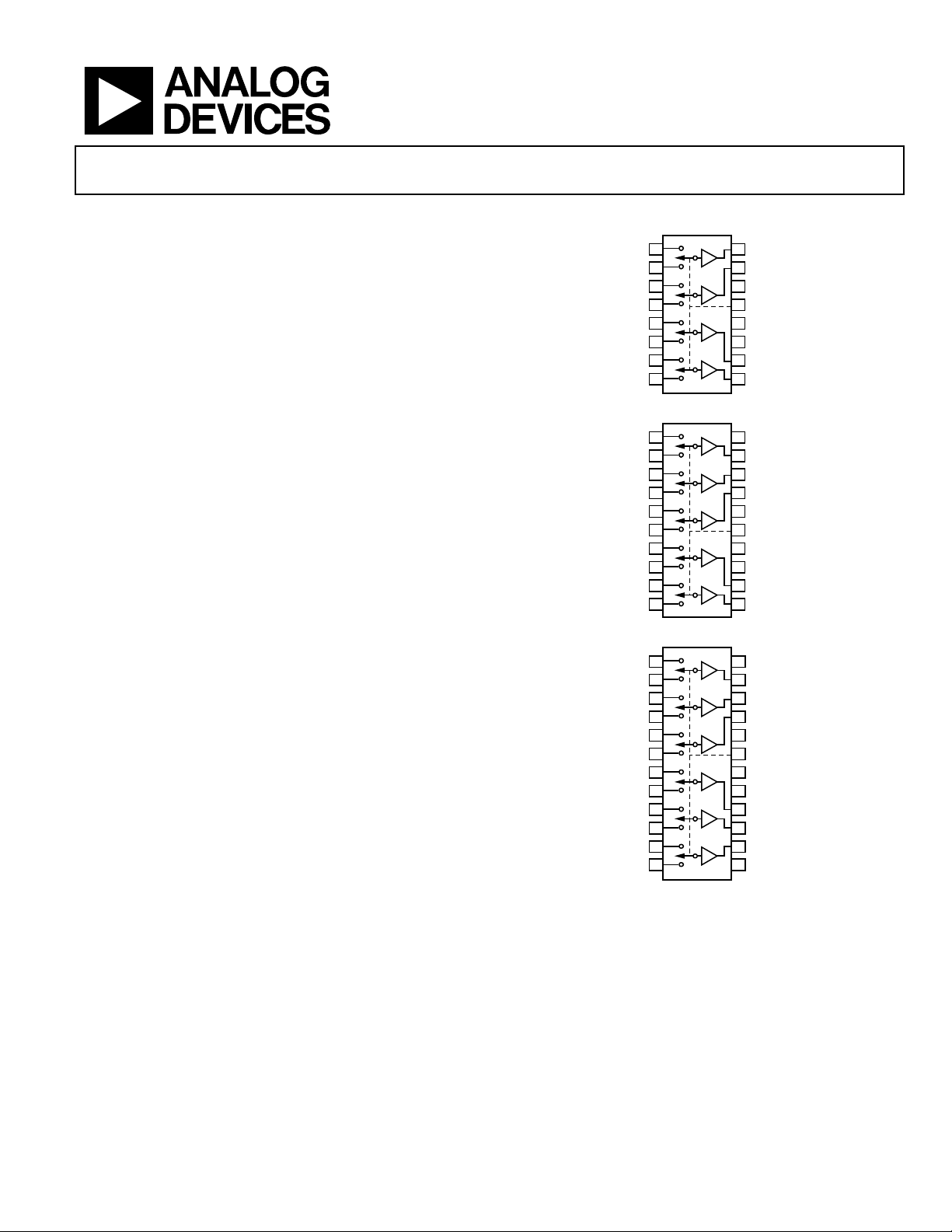
PIN CONFIGURATION DIAGRAMS
INA1
1
INB1
2
INA2
3
INB2
4
INA3
5
INB3
6
INA4
7
INB4
8
Figure 1. ADD8504, 4-Channel Buffer
INA1 1 VCC120
INB1 2 OUT119
INA2 3 OUT218
INB2 4 OUT317
INA3 5 VCC216
INB3 6 A/B15
INA4 7 GND14
INB4 8 GND13
9
INA5
10
INB5
Figure 2. ADD8505, 5-Channel Buffer
INA1
1
INB1
2
3
INA2
INB2
4
INA3
5
6
INB3
INA4
7
INB4
8
INA5
9
INB5
10
11
INA6
INB6
12
Figure 3. ADD8506, 6-Channel Buffer
OUT1
16
OUT2
15
VCC1
14
A/B
13
GND
12
GND
11
OUT3
10
OUT4
9
05549-001
12
OUT4
11
OUT5
05549-002
VCC1
24
OUT1
23
22
OUT2
OUT3
21
VCC2
20
19
A/B
GND
18
GND
17
OUT4
16
OUT5
15
14
OUT6
VCC3
13
05549-003
Rev. D
Information furnished by Analog Devices is believed to be accurate and reliable. However, no
responsibility is assumed by Analog Devices for its use, nor for any infringements of patents or other
rights of third parties that may result from its use. Specifications subject to change without notice. No
license is granted by implication or otherwise under any patent or patent rights of Analog Devices.
Trademarks and registered trademarks are the property of their respective owners.
One Technology Way, P.O. Box 9106, Norwood, MA 02062-9106, U.S.A.
Tel: 781.329.4700 www.analog.com
Fax: 781.461.3113 ©2005–2010 Analog Devices, Inc. All rights reserved.

ADD8504/ADD8505/ADD8506
TABLE OF CONTENTS
Features .............................................................................................. 1
Applications ....................................................................................... 1
General Description ......................................................................... 1
Pin Configuration Diagrams ........................................................... 1
Revision History ............................................................................... 2
Specifications ..................................................................................... 3
Electrical Characteristics ............................................................. 3
Absolute Maximum Ratings ............................................................ 4
Thermal Resistance ...................................................................... 4
REVISION HISTORY
6/10—Rev. C to Rev. D
Change to Features Section, Applications Section, and General
Description Section .......................................................................... 1
Changes to Ordering Guide ............................................................ 9
Added Automotive Ordering Guide and Automotive Products
Section ................................................................................................ 9
9/07—Rev. B to Rev. C
Change to General Description ...................................................... 1
Change to Ordering Guide .............................................................. 9
1/06—Rev. A to Rev. B
Added Pin Configurations and Function
Descriptions Section ........................................................................ 5
Added Table 5 .................................................................................... 8
ESD Performance ..........................................................................4
ESD Caution...................................................................................4
Pin Configurations and Function Descriptions ............................5
Typical Performance Characteristics ..............................................6
Applications Information .................................................................7
Outline Dimensions ..........................................................................8
Ordering Guide .............................................................................9
Automotive Ordering Guide ........................................................9
Automotive Products ....................................................................9
10/05—Rev. 0 to Rev. A
Added ADD8504 and ADD8505...................................... Universal
Changes to Specifications Section ................................................... 3
Updated Outline Dimensions .......................................................... 7
Changes to Ordering Guide ............................................................. 7
9/05—Revision 0: Initial Version
Rev. D | Page 2 of 12

ADD8504/ADD8505/ADD8506
SPECIFICATIONS
ELECTRICAL CHARACTERISTICS
VCC = 5 V, TA = 25°C, unless otherwise noted. VIN denotes buffer input voltage; I
C
denotes load capacitance.
L
Table 1.
Parameter Symbol Conditions Min Typ Max Unit
INPUT CHARACTERISTICS
Offset Voltage VOS 0 V ≤ VIN ≤ 5 V 20 mV
Input Common-Mode Voltage Range V
CM
Input Bias Current IB V
0 5 V
= 2.5 V 2 50 nA
IN
Voltage Gain AVO 0.985 V/V
OUTPUT CHARACTERISTICS
Output Voltage High VOH I
Output Voltage Low VOL I
Output Resistance R
OUT
= +20 mA 4.75 V
LOAD
= −20 mA 0.2 V
LOAD
−20 mA ≤ I
≤ +20 mA; 0.5 V ≤ VIN ≤ 4.5 V 0.20 Ω
LOAD
Output Short-Circuit Current ISC 120 380 mA
POWER SUPPLY
Supply Current ISY V
= 2.5 V
IN
ADD8504 2.7 3.8 mA
ADD8505 3.0 4.4 mA
ADD8506 3.9 5.1 mA
Supply Voltage Range VCC 3.3 6.5 V
DYNAMIC PERFORMANCE
Slew Rate SR CL = 15 pF 7.0 V/μs
R
Settling Time tS C
= 250 Ω 6.2 V/μs
L
= 200 pF, RL = 10 kΩ 2.5 6 μs
L
LOGIC INPUT CHARACTERISTICS
Input Current Low IIL V
Input Current High IIH V
Input Voltage Low VIL V
V
= 0.0 V 100 nA
IN
= 5.0 V 100 nA
IN
= 5.0 V, −40°C ≤ TA ≤ 105°C 0.8 V
CC
= 3.3 V, −40°C ≤ TA ≤ 105°C 0.7 V
CC
Input Voltage High VIH VCC = 5.0 V, −40°C ≤ TA ≤ 105°C 1.7 V
V
= 3.3 V, −40°C ≤ TA ≤ 105°C 1.4 V
CC
denotes load current; RL denotes load resistance;
LOAD
Rev. D | Page 3 of 12
ADD8504/ADD8505/ADD8506
ABSOLUTE MAXIMUM RATINGS
Table 2.
Parameter Rating
Supply Voltage 7 V
Input Voltage GND to VCC
Storage Temperature Range −65°C to +150°C
Junction Temperature Range −65°C to +150°C
Lead Temperature (Soldering, 60 sec) 300°C
Stresses above those listed under Absolute Maximum Ratings
may cause permanent damage to the device. This is a stress
rating only; functional operation of the device at these or any
other conditions above those indicated in the operational
section of this specification is not implied. Exposure to absolute
maximum rating conditions for extended periods may affect
device reliability.
THERMAL RESISTANCE
Table 3. Thermal Package Characteristics
Model Package Type θ
ADD8504WRUZ 16-Lead Pb-Free TSSOP 150 28 °C/W
ADD8505WRUZ 20-Lead Pb-Free TSSOP 143 45 °C/W
ADD8506WRUZ 24-Lead Pb-Free TSSOP 128 45 °C/W
1
θJA is specified for natural convection on a two-layer board.
2
θJC is specified for natural convection on a two-layer board.
1
θ
JA
2
Unit
JC
ESD PERFORMANCE
Table 4.
Model HBM1 MM2 FICDM3
ADD8504WRUZ 4.0 kV 400 V 1.0 kV
ADD8505WRUZ 3.5 kV 200 V 1.0 kV
ADD8506WRUZ 3.5 kV 200 V 1.0 kV
1
Human body model.
2
Machine model.
3
Field induced charge device model.
ESD CAUTION
Rev. D | Page 4 of 12

ADD8504/ADD8505/ADD8506
PIN CONFIGURATIONS AND FUNCTION DESCRIPTIONS
INA1
1
INB1
2
3
INA2
INB2
4
INA3
5
6
INB3
INA4
7
INB4
8
INA5
9
INB5
10
11
INA6
INB6
12
Figure 4. Pin Configuration, ADD8506, 6-Channel Buffer
VCC1
24
OUT1
23
22
OUT2
OUT3
21
VCC2
20
19
A/B
GND
18
GND
17
OUT4
16
OUT5
15
14
OUT6
VCC3
13
05549-003
INA1
INB1
INA2
INB2
INA3
INB3
INA4
INB4
INA5
INB5
1
2
3
4
5
6
7
8
9
10
VCC1
20
OUT1
19
OUT2
18
OUT3
17
VCC2
16
A/B
15
GND
14
GND
13
12
OUT4
11
OUT5
05549-002
Figure 5. Pin Configuration, ADD8505, 5-Channel Buffer
INA1
INB1
INA2
INB2
INA3
INB3
INA4
INB4
1
2
3
4
5
6
7
8
OUT1
16
OUT2
15
VCC1
14
A/B
13
GND
12
GND
11
OUT3
10
OUT4
9
05549-001
Figure 6. Pin Configuration, ADD8504, 4-Channel Buffer
Table 5. Pin Function Descriptions
ADD8506
Pin No.
ADD8505
Pin No.
ADD8504
Pin No.
Mnemonic Function Description
1 1 1 INA1 Input Channel 1 Buffer Input A.
2 2 2 INB1 Input Channel 1 Buffer Input B.
3 3 3 INA2 Input Channel 2 Buffer Input A.
4 4 4 INB2 Input Channel 2 Buffer Input B.
5 5 5 INA3 Input Channel 3 Buffer Input A.
6 6 6 INB3 Input Channel 3 Buffer Input B.
7 7 7 INA4 Input Channel 4 Buffer Input A.
8 8 8 INB4 Input Channel 4 Buffer Input B.
9 9 N/A INA5 Input Channel 5 Buffer Input A.
10 10 N/A INB5 Input Channel 5 Buffer Input B.
11 N/A N/A INA6 Input Channel 6 Buffer Input A.
12 N/A N/A INB6 Input Channel 6 Buffer Input B.
13 N/A N/A VCC3 Power In Power Supply Input. Short to VCC1 and VCC2. Typically connected to 5 V.
14 N/A N/A OUT6 Output Channel 6 Buffer Output.
15 11 N/A OUT5 Output Channel 5 Buffer Output.
16 12 9 OUT4 Output Channel 4 Buffer Output.
17, 18 13, 14 11, 12 GND Ground Ground.
19 15 13 A/B Input Switch Control. Logic High selects Input A; Logic Low selects Input B.
20 16 N/A VCC2 Power In Power Supply Input. Short to VCC1 and VCC3. Typically connected to 5 V.
21 17 10 OUT3 Output Channel 3 Buffer Output.
22 18 15 OUT2 Output Channel 2 Buffer Output.
23 19 16 OUT1 Output Channel 1 Buffer Output.
24 20 14 VCC1 Power In Power Supply Input. Short to VCC2 and VCC3. Typically connected to 5 V.
Rev. D | Page 5 of 12

ADD8504/ADD8505/ADD8506
TYPICAL PERFORMANCE CHARACTERISTICS
5.5
VCM = 2.5V
T
= 25°C
5.0
A
4.5
4.0
3.5
3.0
2.5
2.0
SUPPLY CURRENT (mA)
1.5
1.0
0.5
0
1000
100
123456
0
SUPPLY VOLTAGE (V)
Figure 7. Supply Current vs. Supply Voltage
VCC = 5V
T
= 25°C
A
7
05549-004
5V
INPUT
OUTPUT
CH1 2.00V CH2 2.00V M400ns
0V
5V
Figure 10. Transient Response—Rising
INPUT
VCC = 5V
T
= 25°C
A
0V
05549-007
5V
VCC = 5V
T
= 25°C
A
OUTPUT HIGH
10
Δ OUTPUT VOLTAGE TO SUPPLY RAIL (mV)
1
0.1
110
LOAD CURRENT (mA)
OUTPUT LOW
Figure 8. Δ Output Voltage to Supply Rail vs. Load Current
6
CH6
4
CH2
2
CH5
0
CH3
(mV)
OS
–2
V
CH1
–4
–6
CH4
–8
–40
0 2540809095100105
TEMPERATURE (°C)
Figure 9. Offset Voltage vs. Temperature
VCC = 5V
V
= 2.5V
CM
100
05549-005
05549-006
0V
OUTPUT
CH1 2.00V CH2 2.00V M400ns
Figure 11. Transient Response—Falling
5V
0V
05549-008
Rev. D | Page 6 of 12

ADD8504/ADD8505/ADD8506
APPLICATIONS INFORMATION
The ADD8504/ADD8505/ADD8506 have CMOS buffers with
A/B inputs to select between two different reference voltages set
up by an external resistor ladder. Input bias currents are orders
of magnitude less than competitive parts. This allows the use of
a very large resistor ladder to save supply current.
The buffer outputs are designed to drive resistive or capacitive
loads. Therefore, to attain the best display performance, do not
use resistors in series with these outputs. Outputs have high
slew rates and 6 μs settling times. Each output delivers a minimum of 120 mA, ensuring a fast response to varying loads.
5V
Power supply pins on the ADD8505 and ADD8506 have
multiple ground (GND) and supply (VCC) connections.
Because of the high peak currents that these buffers deliver, it
is recommended that all GND and VCC pins be connected and
suitably bypassed.
Table 6. Mux Function
A/B Select Input
Logic High INAx
Logic Low INBx
VCOM
(INVERTING SIGNAL)
5V
0.1μF
RA1
RA2
RA3
RA4
RA5
RA6
RA7
NOTES
1. RAx RESISTORS ARE USED TO SET POSITIVE INVERSION GAMMA VOLTAGES.
2. RBx RESISTORS ARE USED TO SET NEGATIVE INVERSION GAMMA VOLTAGES.
RB1
RB2
RB3
RB4
RB5
RB6
RB7
5V
0.1μF
1
2 23
3 22
4 21
5 20
6 19
7 18
8 17
9 16
10 1510
10 1411
12 13
24
0.1μF
TO COLUMN
DRIVERS
Figure 12. ADD8506 Typical Application
05549-009
Rev. D | Page 7 of 12

ADD8504/ADD8505/ADD8506
Y
OUTLINE DIMENSIONS
5.10
5.00
4.90
0.15
0.05
4.50
4.40
4.30
PIN 1
16
0.65
BSC
COPLANARITY
COMPLIANT TO JEDEC STANDARDS MO-153-AB
0.10
0.30
0.19
9
81
1.20
MAX
SEATING
PLANE
6.40
BSC
0.20
0.09
Figure 13. 16-Lead Thin Shrink Small Outline Package [TSSOP]
(RU-16)
Dimensions shown in millimeters
6.60
6.50
6.40
PIN 1
0.15
0.05
COPLANARIT
20
1
0.65
BSC
0.30
0.19
0.10
COMPLIANT TO JEDEC STANDARDS MO-153-AC
1.20 MAX
11
10
SEATING
PLANE
4.50
4.40
4.30
6.40 BSC
0.20
0.09
Figure 14. 20-Lead Thin Shrink Small Outline Package [TSSOP]
(RU-20)
Dimensions shown in millimeters
8°
0°
0.75
0.60
0.45
8°
0°
0.75
0.60
0.45
7.90
7.80
7.70
24
PIN 1
0.15
0.05
0.10 COPLANARITY
0.65
BSC
0.30
0.19
COMPLIANT TO JEDEC STANDARDS MO-153-AD
13
121
1.20
MAX
SEATING
PLANE
4.50
4.40
4.30
6.40 BSC
0.20
0.09
8°
0°
0.75
0.60
0.45
Figure 15. 24-Lead Thin Shrink Small Outline Package [TSSOP]
(RU-24)
Dimensions shown in millimeters
Rev. D | Page 8 of 12

ADD8504/ADD8505/ADD8506
ORDERING GUIDE
Te mp e ra tu r e
Model1
ADD8504WRUZ −40°C to +105°C 16-Lead Thin Shrink Small Outline Package [TSSOP], Tube RU-16 96
ADD8504WRUZ-REEL7 −40°C to +105°C 16-Lead Thin Shrink Small Outline Package [TSSOP], 7” Tape and Reel RU-16 1,000
ADD8504WRUZ-REEL −40°C to +105°C 16-Lead Thin Shrink Small Outline Package [TSSOP], 13” Tape and Reel RU-16 2,500
ADD8505WRUZ −40°C to +105°C 20-Lead Thin Shrink Small Outline Package [TSSOP], Tube RU-20 75
ADD8505WRUZ-REEL7 −40°C to +105°C 20-Lead Thin Shrink Small Outline Package [TSSOP], 7” Tape and Reel RU-20 1,000
ADD8505WRUZ-REEL −40°C to +105°C 20-Lead Thin Shrink Small Outline Package [TSSOP], 13” Tape and Reel RU-20 2,500
ADD8506WRU-REEL7 −40°C to +105°C 24-Lead Thin Shrink Small Outline Package [TSSOP], 7” Tape and Reel RU-24 1,000
ADD8506WRUZ −40°C to +105°C 24-Lead Thin Shrink Small Outline Package [TSSOP], Tube RU-24 62
ADD8506WRUZ-REEL7 −40°C to +105°C 24-Lead Thin Shrink Small Outline Package [TSSOP], 7” Tape and Reel RU-24 1,000
ADD8506WRUZ-REEL −40°C to +105°C 24-Lead Thin Shrink Small Outline Package [TSSOP], 13” Tape and Reel RU-24 2,500
ADD8504-EVAL Evaluation Board
ADD8505-EVAL Evaluation Board
ADD8506-EVAL Evaluation Board
1
Z = RoHS Compliant Part.
Range Package Description
AUTOMOTIVE ORDERING GUIDE
Te mp e ra tu r e
Automotive Model1
ADD8506WWARUZR7 −40°C to +105°C 24-Lead Thin Shrink Small Outline Package [TSSOP], 7” Tape and Reel RU-24 1,000
1
Qualified for automotive applications.
Range Package Description
Package
Option
Package
Option
Ordering
Quantity
Ordering
Quantity
AUTOMOTIVE PRODUCTS
The ADD8506WWARUZR7 model is available with controlled manufacturing to support the quality and reliability requirements of
automotive applications. Note that the automotive model may have specifications that differ from the commercial models; therefore,
designers should review the Specifications section of this data sheet carefully. Only the automotive grade product shown is available for
use in automotive applications. Contact your local Analog Devices account representative for specific product ordering information and
to obtain the specific Automotive Reliability reports for this model.
Rev. D | Page 9 of 12

ADD8504/ADD8505/ADD8506
NOTES
Rev. D | Page 10 of 12

ADD8504/ADD8505/ADD8506
NOTES
Rev. D | Page 11 of 12

ADD8504/ADD8505/ADD8506
NOTES
©2005–2010 Analog Devices, Inc. All rights reserved. Trademarks and
registered trademarks are the property of their respective owners.
D05549-0-6/10(D)
Rev. D | Page 12 of 12
 Loading...