

Integrated LCD
a
FEATURES
Two Mask Programmable Sets of Five Reference Levels
Dual 10-Bit DACs for Flicker Offset and Range Adjustment
Integrated V
Single-Supply Operation: 5.0 V
Low Supply Current: 300 A
Global Power Save Mode: 1 A Max
Fast Settling Time for Load Change: 20 s
Stable with 20 nF/100 Loads
CMOS/TTL Input Levels
APPLICATIONS
Color TFT Cell Phones
Color TFT PDAs
GENERAL DESCRIPTION
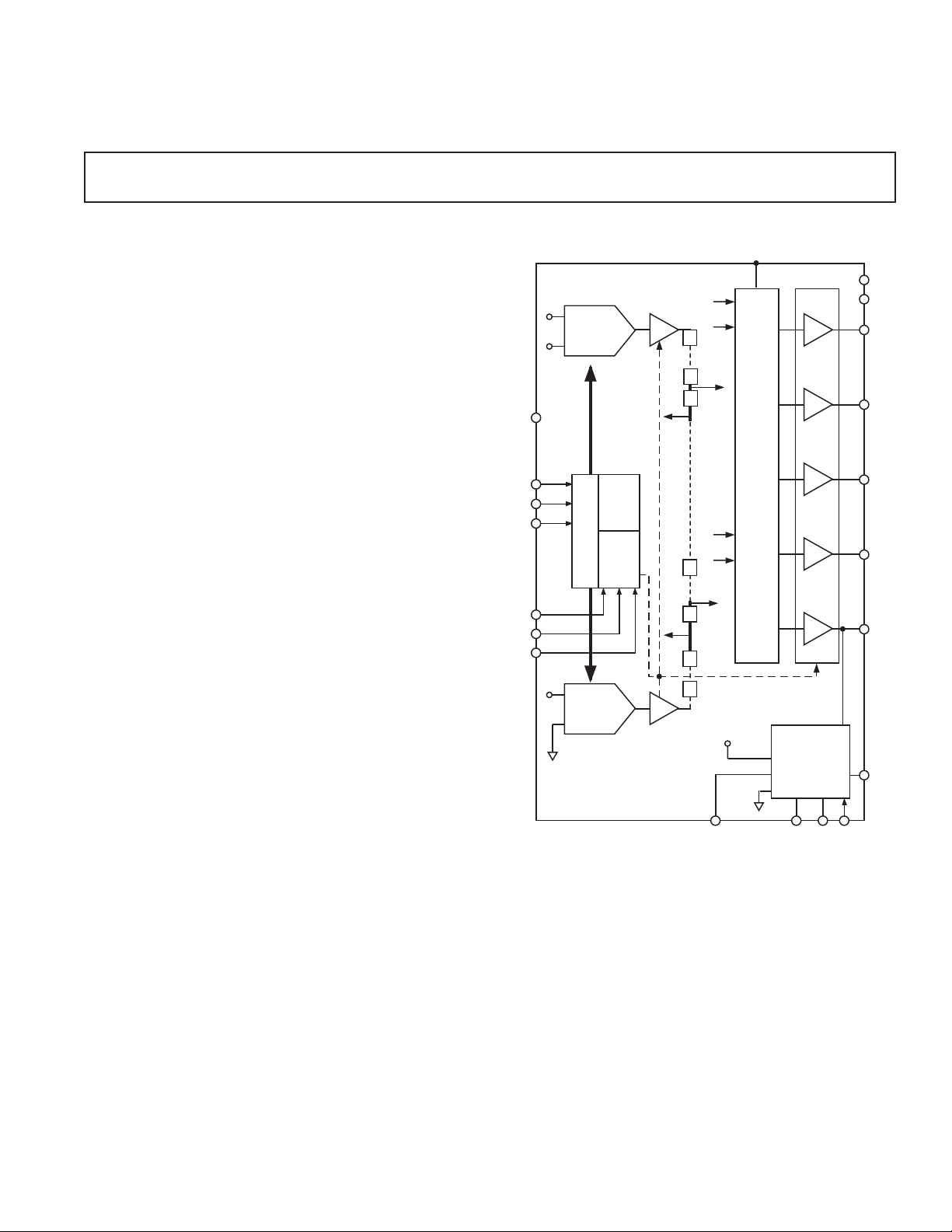
The ADD8502 is an integrated, high accuracy, programmable
grayscale generator. Two sets of five output reference voltages
are mask programmed to 0.2% resolution. The outputs switch
between the two sets of five levels. The reference levels are selected
from a 512 tap resistor network using a via mask.
ADD8502 includes two serially addressable, 10-bit digital-toanalog converters (DACs) and five fast, low current buffers.
The dual DACs set the endpoint voltages applied to the resistor
network to adjust for flicker and range. The two power save modes
can reduce the total current to less than 1 µA and feature fast
recovery time from Shutdown/Sleep Mode. The ADD8502
accepts CMOS or TTL inputs for all controls, including the
common drive circuit levels.
ADD8502 operates over the industrial temperature range from
–40°C to +85°C and is available in a space-saving 24-lead
4 mm 4 mm frame chip scale package.
Switching
COM
SCK
D
CS-LD
PSK
GS1
GS2
Grayscale Generator
ADD8502
FUNCTIONAL BLOCK DIAGRAM
REV2
V
V
DD
VREF+
VREF–
VREF+
VREF–
10-BIT
DAC A
DIGITAL
CORE
POWER
SAVE
LOGIC
INTERFACE LOGIC
10-BIT
DAC B
VN4
VN0
VDD/2
V
L
IN
VDD/2
VP0
VN0
R
VP0
R
R
MUX
VP4
VN4
R
VP4
R
R
R
V
DD
A0
A1
A2
A3
A4
V
COM
LOGIC
DD
GND
V0
V1
V2
V3
V4
COM
REV. 0
Information furnished by Analog Devices is believed to be accurate and
reliable. However, no responsibility is assumed by Analog Devices for its
use, nor for any infringements of patents or other rights of third parties
that may result from its use. No license is granted by implication or
otherwise under any patent or patent rights of Analog Devices.
CMREV1COM_M
CV4
One Technology Way, P.O. Box 9106, Norwood, MA 02062-9106, U.S.A.
Tel: 781/329-4700 www.analog.com
Fax: 781/326-8703 © Analog Devices, Inc., 2002
ADD8502–SPECIFICATIONS
(@ VDD = 5.0 V, 40C ≤ TA ≤ 85C, unless otherwise noted.)
Parameter Symbol Conditions Min Typ Max Unit
SYSTEM ACCURACY
Error 320 mV
V
OUT
Swing Error
Mean Error
Mean Error between Adjacent Channels
Mean Error between V0 and V4
1
2
3
4
(VPn – VNn) – (VPi – VNi)117mV
(VPn+ VNn)/2 – (VPi + VNi)/2) 3 21 mV
321 mV
325 mV
DAC ACCURACY
Resolution 10 Bits
Differential Nonlinearity DNL ±0.25 LSB
Integral Nonlinearity
5
INL ±0.5 LSB
Offset Error ±0.4 % of FSR
Gain Error ±0.15 % of FSR
OUTPUT CHARACTERISTICS
Output Current I
Short Circuit Current I
Output Leakage Current in High-Z Mode I
OUT
SC
LEAKAGE
Slew Rate SR R
Settling Time to 1% t
Slew Rate
Settling Time to 1%
5
5
S
SR LD =100 Ω Series 16 nF 0.7 V/µs
t
S
(VDD – 1 V) 25 mA
Short to Ground 60 mA
High-Z Mode 0.01 1.0 µA
= 100 kΩ 1.25 V/µs
L
V0 to V4 Step Size 8 12 µs
V0 to V4 Step Size 8 12 µs
Phase Margin φo67Degrees
SWITCHES ACTIVE IMPEDANCE
V
COM
COM to V
DD
Z See Table IV 25 50 Ω
COM to GND Z 25 50 Ω
COM to COM_M Z I = 20 mA 25 50 Ω
COM to V4 Z 25 50 Ω
MASK PROGRAMMABLE
RESISTOR CHAIN
Resistor Matching R
MATCH
Any Two Segments between 1 %
512 Resistor String
POWER SUPPLY
Supply Voltage V
Supply Current I
Shutdown Supply Current I
Sleep Supply Current I
DD
SY
SY-GLB
SY-GS1-3
VDD = 5 V; No Load 190 270 400 µA
Full Shutdown Mode 0.2 1 µA
Mid 3 Buffers Shutdown 140 175 210 µA
4.5 5 5.5 V
Shutdown Recovery Time Global PD to 1% 23 30 µs
Sleep Recovery Time V1–V3 Off to 1% 10 15 µs
LOGIC SUPPLY
Logic Input Voltage Level V
Logic Input Current I
L
VL
2.3 3.3 5.5 V
0.01 1 µA
DIGITAL I/O
Digital Input High Voltage V
Digital Input Low Voltage V
Digital Input Current I
Digital Input Capacitance C
NOTES
1
Swing error is a comparison of measured V
2
Mean error is measured V
3
Mean errors between two adjacent channels versus theoretical (see Figure 3).
4
Mean errors between V0 and V4 versus theoretical (see Figure 3).
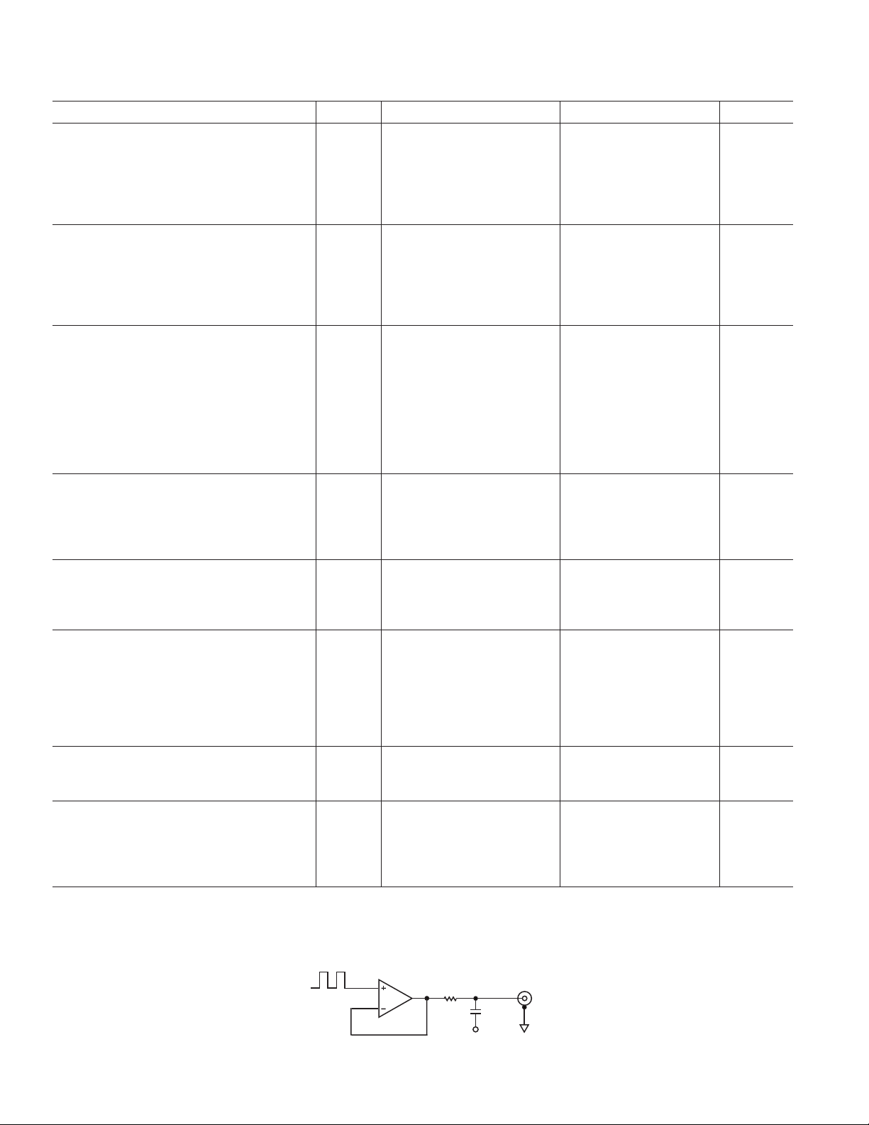
5
Slew rate and settling time are measured between the output resistor and the capacitor (see Figure 1) .
Specifications subject to change without notice.
mean versus theoretical V
OUT
step versus theoretical V
OUT
IH
IL
IN
IN
mean (see Figure 3).
OUT
GND ≤ VIN ≤ 5.5 V ±1 µA
step. Theoretical values can be found on the Mask Tap Point Option sheet.
OUT
R
L
100
16nF
V
COM
C
L
VL 0.7 V
VL 0.3 V
10 pF
Figure 1. Slew Rate Diagram
–2–
REV. 0
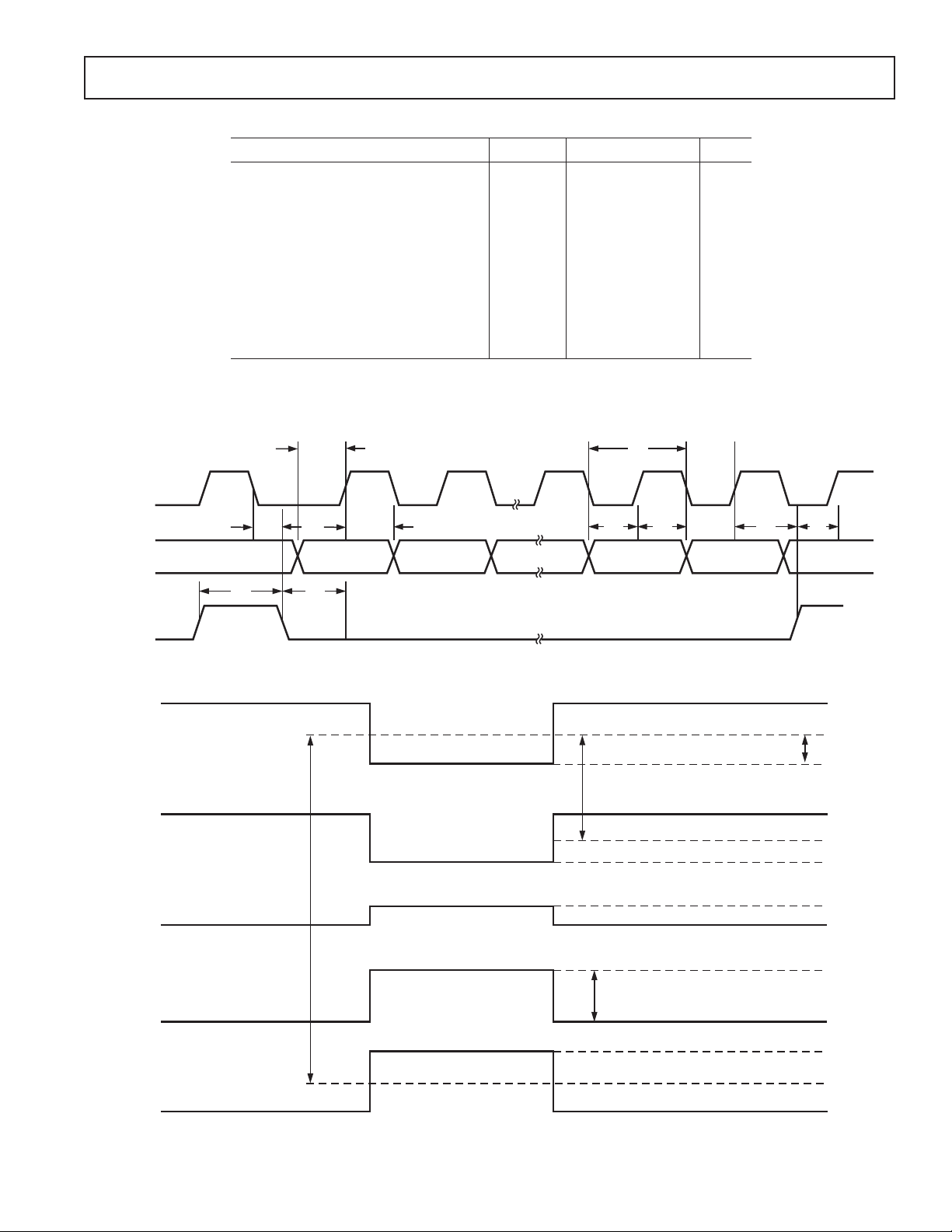
Table I. Serial Data Timing Characteristics
Parameter Symbol Min Typ Max Unit
SCK Cycle Time t
SCK High Time t
SCK Low Time t
CS-LD Setup Time t
Data Setup Time t
Data Hold Time t
LSB SCK High to CS-LD High t
Minimum CS-LD High Time t
SCK to CS-LD Active Edge Setup Time t
CS-LD High to SCK Positive Edge t
1
2
3
4
5
6
7
8
9
10
100 ns
45 ns
45 ns
20 ns
5ns
5ns
5ns
10 ns
5ns
10 ns
SCK Frequency (Square Wave) 10 MHz
NOTES
1
All input signals are specified with rise/fall time –5 ns (10% to 90% of VDD) and timed from a voltage level
of (VS + VIH)/2.
2
See Figure 2.
ADD8502
SCK
CS-LD
t
5
t
9
IN
t
8
t
4
t
6
C3 C2 X1 X0D
t
1
t
t
3
2
t
7
t
10
Figure 2. Serial Write Interface
VO
SEE NOTE 2 ON SPECIFICATIONS TABLE
V0 – V1
SEE NOTE 3 ON SPECIFICATIONS TABLE
V1
SEE NOTE 4 ON
SPECIFICATIONS TABLE
V2
VP0
VN0
VP1
VN1
VN2
VP2
REV. 0
VN3
SEE NOTE 1 ON SPECIFICATIONS TABLE
V3
V4
VP3
VN4
VP4
Figure 3. Output Wave Form Diagram
–3–
ADD8502
WARNING!
ESD SENSITIVE DEVICE
ABSOLUTE MAXIMUM RATINGS*
VDD to GND . . . . . . . . . . . . . . . . . . . . . . . . . . –0.3 V to +7 V
V
to GND . . . . . . . . . . . . . . . . . . . . . . . . . . . –0.3 V to +7 V
L
Digital Input Voltage to GND . . . . . . . . . . . . . –0.3 V to +7 V
to GND . . . . . . . . . . . . . . . . . . . . –0.3 V to VDD +0.3 V
V
OUT
V
to GND . . . . . . . . . . . . . . . . . . . . –0.3 V to VDD +0.3 V
COM
Storage Temperature Range . . . . . . . . . . . . –65°C to +150°C
Lead Temperature Range (Soldering, 10 sec)
Package Type
24-Lead LFCSP (ACP) 34.8 13 °C/W
NOTES
1
θJA is specified for worst-case conditions, i.e., θ
in circuit board for surface-mount packages.
2
ψJB is applied for calculating the junction temperature by reference to the board
temperature.
Vapor Phase (60 sec) . . . . . . . . . . . . . . . . . . . . . . . . . 300°C
*Stresses above those listed under Absolute Maximum Ratings may cause
permanent damage to the device. This is a stress rating only; functional operation
of the device at these or any other conditions above those listed in the operational
sections of this specification is not implied. Exposure to absolute maximum
rating conditions for extended periods may affect device reliability.
Model Range Description Option
ORDERING GUIDE
Temperature Package Package
ADD8502ACP –40°C to +85°C24-Lead LFCSP CP-24
Available in 7” reel only.
CAUTION
ESD (electrostatic discharge) sensitive device. Electrostatic charges as high as 4000 V readily
accumulate on the human body and test equipment and can discharge without detection. Although
the ADD8502 features proprietary ESD protection circuitry, permanent damage may occur on
devices subjected to high energy electrostatic discharges. Therefore, proper ESD precautions are
recommended to avoid performance degradation or loss of functionality.
1
JA
JA
2
JB
is specified for device soldered
Unit
–4–
REV. 0
ADD8502
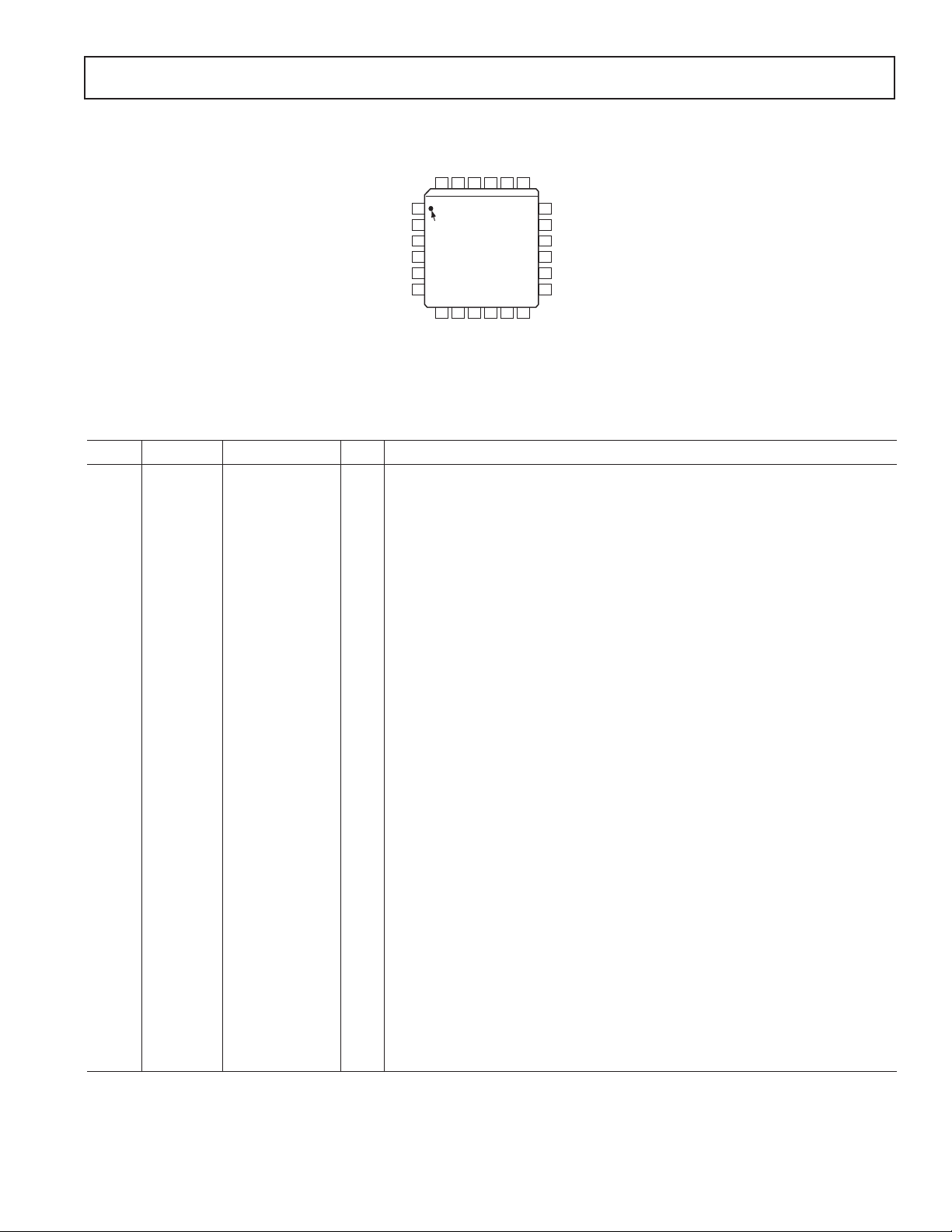
PIN CONFIGURATION
DD
REV2
COM
V
NC
NC
COM_M
18
V0
V1
17
16
V2
V3
15
14
V4
13
GND
DD.
input into the
IN
when REV1 is HIGH and will output
DD
PSK
GS1
GS2
24
23 22 21 20 19
1
V
L
PIN 1
2
D
IN
IDENTIFIER
3
SCK
CS-LD
CM
CV4
ADD8502
4
TOP VIEW
(Not to Scale)
5
6
789101112
NC
NC
REV1
NC = NO CONNECT
PIN FUNCTION DESCRIPTIONS
Pin No. Mnemonic Name I/O Description
1V
L
Logic Select Pin I Logic Supply Voltage. Connect to supply used for system logic. Can accept 2.7 V to V
2DINSerial Data Input I When CS is LOW, the input on this pin is shifted into the internal shift register on
the rising edge of SCK.
3 SCK Serial Clock I Accepts up to 10 MHz input. The rising edge on this clock will shift the data on
Pin into the internal shift registers.
D
IN
4 CS-LD Load I When CS-LD is LOW, SCK is enabled for shifting data on the D
internal shift register on the rising edge of SCK. Data is loaded MSB first.
5CMLogic Control 2 I When CM is LOW, COM will output the voltage level input on COM_M.
for V
COM
When CM is HIGH, COM levels will be determined by the input on REV1.
6 CV4 Logic Control V4 I If CV4 is HIGH, V4 output is the output of the op amp A4. If CV4 is LOW, V4 is
connected to COM and op amp A4 is shut down. Refer to Table II.
7 REV1 Logic Control 1 I With CM HIGH, a HIGH on REV1 will cause COM to output the voltage level
for V
COM
input at VDD. A LOW on REV1 will cause COM to output the voltage level input
at GND.
8NCNo Connect Unused Pin
9NCNo Connect Unused Pin
10 COM Common Output O If CM is LOW, COM will output the voltage input at COM_M. If CM is HIGH,
COM will output the voltage input at V
the voltage input at GND when REV1 is LOW. Refer to Table II.
11 COM_M Common System I COM_M is a system voltage reference input between 2.5 V and 3.5 V. This may
V
REF
be the system 3.3 V supply.
12 NC No Connect Unused Pin
13 GND Ground I Ground. Nominally 0 V.
14 V4 Output O Buffers are rail-to-rail buffers that can drive high capacitive loads (>16.5 nF).
When PSK is LOW, these outputs will be Hi-Z.
15 V3 Output O Buffers are rail-to-rail buffers that can drive high capacitive loads (>16.5 nF).
When PSK is LOW or GS1 and GS2 = HIGH, these outputs will be Hi-Z.
16 V2 Output O Buffers are rail-to-rail buffers that can drive high capacitive loads (>16.5 nF).
When PSK is LOW or GS1 and GS2 = HIGH, these outputs will be Hi-Z.
17 V1 Output O Buffers are rail-to-rail buffers that can drive high capacitive loads (>16.5 nF).
When PSK is LOW or GS1 and GS2 = HIGH, these outputs will be Hi-Z.
18 V0 Output O Buffers are rail-to-rail buffers that can drive high capacitive loads (>16.5 nF).
When PSK is LOW, these outputs will be Hi-Z.
19 V
DD
Supply I Supply Voltage. Nominally 5 V.
20 NC No Connect Unused Pin
REV. 0
–5–

ADD8502
Pin No. Mnemonic Name I/O Description
21 REV2 Reference Output I When PSK is HIGH and GS1 or GS2 is LOW, then INVERT selects the output
Select levels on V0 to V4. If INVERT is HIGH, outputs V0 to V4 are connected to
reference levels VP0 to VP4, respectively. If INVERT is LOW, outputs V0 to V4
are connected to reference levels VN0 to VN4, respectively. When PSK is HIGH
and GS1 and GS2 are HIGH, V1–V3 are, Hi-Z state, but V0 and V4 are still
connected to reference levels VP0 and VP4 when INVERT is HIGH. Outputs V0
and V4 switch to VN0 and VN4 when REV is LOW.
22 GS2 Sleep Mode I When GS1 and GS2 are HIGH, the middle three output buffers are shut down
Select and V1, V2, and V3 are put into Hi-Z states. Other combinations of GS1 and GS2
leave the outputs of A1 to A3 fully active.
23 GS1 Sleep Mode I When GS1 and GS2 are HIGH, the middle three output buffers are shut down
Select and V1, V2, and V3 are Hi-Z. Other combinations of GS1 and GS2 leave the
outputs of A1 to A3 fully active.
24 PSK Global Power I When PSK is pulled LOW, the chip will be put into the full Power-Down Mode.
Shutdown The DACs, resistor ladder network preamps, and output buffers will all be shut
down, and A0 to A4 will be in Hi-Z states. Recovery from full power-down to
normal operation is within 30 µs.
All digital inputs accept CMOS or TTL logic levels.
–6–
REV. 0

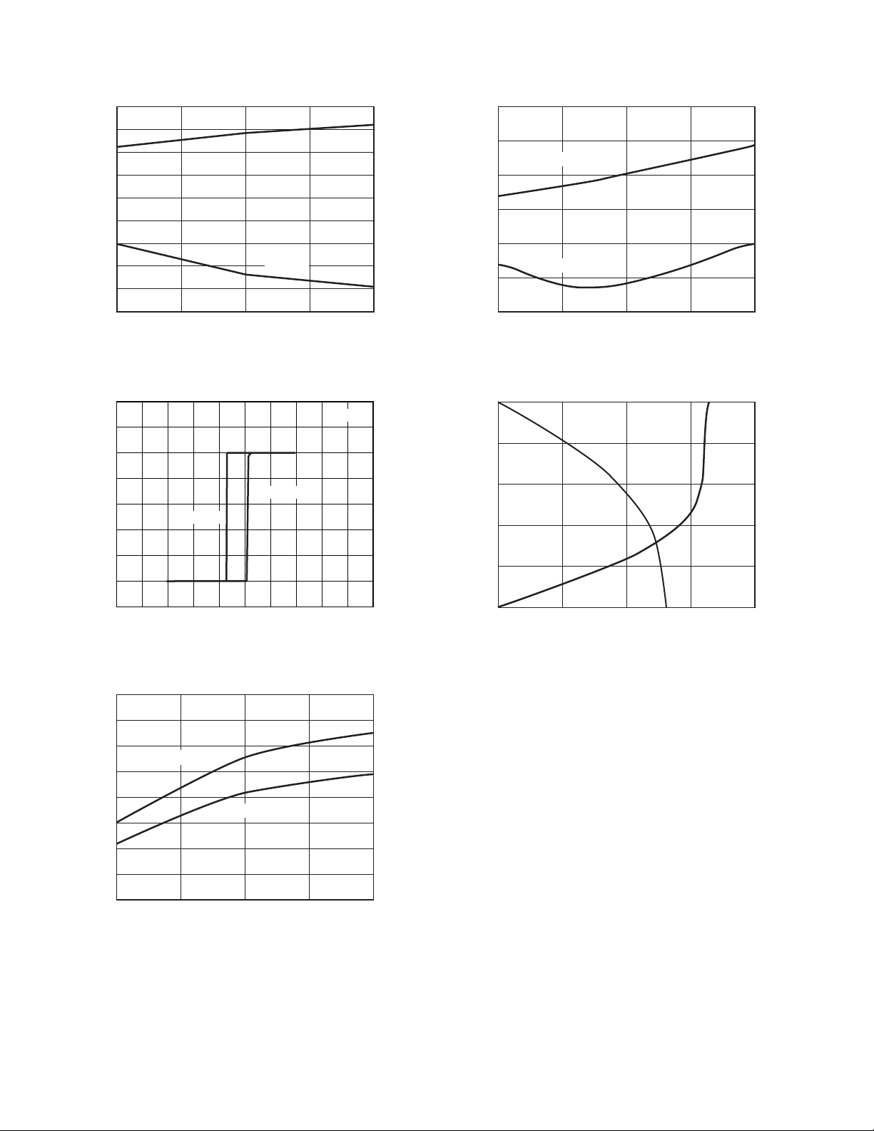
4
TEMPERATURE – C
190
175
155
40
SLEEP SUPPLY CURRENT – A
25 85
165
160
170
V
DD
= 5V
180
185
TEMPERATURE – C
350
200
0
40
SUPPLY CURRENT – A
25 85
100
50
150
V
DD
= 5V
250
300
Typical Performance Characteristics–
ADD8502
5
VDD = 5V
3
1
–1
–3
INTEGRAL NONLINEARITY – %LSB
–5
0 1025128
DAC A
256 384 512 640 768 896
TPC 1. DAC Integral Nonlinearity
5
DAC A
3
1
CODE – LSB
DAC B
VDD = 5V
250
VDD = 5V
200
150
100
SHUTDOWN CURRENT – A
50
0
40
25 85
TEMPERATURE – C
TPC 4. Shutdown Current vs. Temperature
1
3
DIFFERENTIAL NONLINEARITY – %LSB
5
0 102
128
256 384 512 640 768 896
CODE – LSB
TPC 2. DAC Differential Nonlinearity
0.5
0
0.5
1.0
1.5
2.0
OFFSET ERROR – LSB
2.5
3.0
40
TEMPERATURE – C
DAC A
DAC B
25 85
TPC 3. Offset Error vs. Temperature
DAC B
TPC 5. Sleep Supply Current vs. Temperature
VDD = 5V
TPC 6. Supply Current vs. Temperature
REV. 0
–7–

ADD8502
350
300
250
200
150
SYSTEM SUPPLY CURRENT – A
100
273
45 6
VDD – V
TPC 7. System Supply Current at Full Power
400
350
300
250
200
10.0
= 5V
V
DD
9.5
9.0
8.5
8.0
SLEEP RECOVERY TIME – s
7.5
7.0
40
25 85
TEMPERATURE – C
TPC 10. Sleep Recovery Time vs. Temperature
10
VDD = 5V
8
6
4
150
100
SYSTEM SUPPLY CURRENT – nA
50
0
2.0 7.02.5
3.0 3.5 4.0 4.5 5.0 5.5 6.0 6.5
VDD –V
TPC 8. System Supply Current at Shutdown
28
27
26
25
24
23
22
21
20
SHUTDOWN RECOVERY TIME – s
19
18
40
25 85
TEMPERATURE – C
V
= 5V
DD
TPC 9. Shutdown Recovery Time vs. Temperature
LEAKAGE – nA
2
0
2
40
25 85
TEMPERATURE – C
TPC 11. Output Leakage
0
0
0
0
0
0
VOLTA GE – 2V/DIV
0
0
0
000
00000000
TIME – 10s/DIV
VDD = 5V
REV2
V0
TPC 12. V0 Output Swing Response to REV2
–8–
REV. 0

25
OUTPUT VOLTAGE MEAN ERROR
400
150
0
–15 15–13
FREQUENCY
–9 –5 –3 –1 135791113
350
200
100
50
300
250
–11 –7
TEMPERATURE – C
1.5
40
MEAN ERROR BETWEEN ADJACENT CHANNEL – mV
25 85
–0.5
0.5
2.0
0
–1.0
1.0
VP3–VP4
VP0–VP1
VP2–VP3
VP1–VP2
TEMPERATURE – C
0.6
1.4
40
MEAN ERROR CHANNEL-TO-CHANNEL – mV
25 85
0.4
1.0
0.8
0.6
0.4
0.2
0
VN2–VN3
VN3–VN4
VN0–VN1
VN1–VN2
0.2
1.2
20
15
–
ON
R
10
5
0
40
TPC 13. V
800
700
600
500
V
= 5V
DD
25 85
TEMPERATURE – C
Switch-On-Resistance vs. Temperature
COM
TPC 16. V
ADD8502
Swing Mean vs. Distribution
OUT
400
FREQUNECY
300
200
100
0
–23 22–18
–13 –8 –3 2 7 12 17
TPC 14. V
2.0
1.5
1.0
0.5
0
–0.5
–1.0
SWING ERROR – mV
–1.5
REV. 0
–2.0
–2.5
40
TPC 15. Swing Error vs. Temperature
OUTPUT VOLTAGE – mV
Error Distribution
OUT
25 85
TEMPERATURE – C
TPC 17. Mean Error between Adjacent Channel
vs. Temperature
V0
V1
V2
V3
V4
TPC 18. Mean Error between Adjacent Channel
vs. Temperature
–9–
ADD8502
2.0
1.5
1.0
0.5
0
0.5
1.0
MEAN ERROR V0–V4 – mV
1.5
2.0
2.5
40
TEMPERATURE – C
VP0–VP4
VN0–VN4
25 85
TPC 19. Mean Error between V0 and V4 vs. Temperature
0
0
0
0
0
0
VOLTA GE – 500mV/DIV
0
0
VTH HIGH
VTH LOW
VL = 2.5V
10
9
RISING EDGE
8
s
7
TIME –
6
5
4
40
FALLING EDGE
45 125
TEMPERATURE – C
TPC 22. Settling Time at V
5
4
3
2
OUTPUT VOLTAGE – V
1
SOURCE
VDD = 5V
vs. Temperature
OUT
SINK
0
000
00000000
TIME – 500mV/DIV
TPC 20. REV1 Hysteresis
1.40
1.35
1.30
SLEW RATE FALLING
1.25
1.20
1.15
SLEW RATE – V/s
1.10
1.05
1.00
40
SLEW RATE RISING
25 85
TEMPERATURE – C
TPC 21. Slew Rate vs. Temperature
VDD = 5V
0
08020
OUTPUT CURRENT – mA
40 60
TPC 23. Output Current Source and Sink
–10–
REV. 0

ADD8502
OPERATION
Transfer Function
The transfer function for the ADD8502 is given in the following
equations:
1. Digital-to-analog transfer function for DAC A. An output can
be derived from Equation 1 as:
V
OUTA
DD A
=
2
1
+
(1)
1024
VD
2. Digital-to-analog transfer function for DAC B. An output can
be derived from Equation 2 as:
DV
Where D
and DB are decimal equivalents of the binary codes
A
V
OUTB
BDD
=
1024 2
(2)
that are loaded to the DAC Register from 0 to 1023.
3. Using any programmed tap point from the 512 resistor string,
the system output can be derived from Equation 3:
T
VV V
=−
TX OUTA OUTB
512
X
V
+( )
(3)
OUTB
Where TX is any tap point of the 512 resistor string. It is mask
programmable. V
is the voltage output at any output (VO, ... V4)
TX
and will switch between two voltages depending on the mask
programmed tap points.
Example: V
= 5 V, DA = 1,000, DB = 100, and TX = 500.
DD
V
= 4.941 V
OUTA
V
= 0.244 V
OUTB
V
= 4.831 V
TX
Equations 1–3 will provide a theoretical calculation of the outputs. The actual will vary with load, process, and architecture.
See Specifications table.
SERIAL INTERFACE
The ADD8502 has a 3-wire serial interface (CS-LD, SCK, and
D
). The writing sequence begins by bringing the CS-LD line
IN
LOW. Data on the D
line is clocked into the 16-bit shift regis-
IN
ter on the rising edge of SCK. The serial clock frequency can be
as high as 10 MHz. When the last data bit is clocked in,
CS-LD line needs to be brought HIGH to load the DAC registers and the operation mode is dependent upon the control bits.
Input Shift Register
The input shift register is 16 bits wide (see Figure 4). The first
four control bits (C3, C2, C1, and C0) are used to set the different
operating modes of the device. The next 10 bits are the data bits
and the last two bits are “Don’t Cares.” This composes a full word
that is transferred to the DAC register on the rising edge of CS-LD.
In a normal write sequence, the CS-LD line is kept LOW for at
least 16 rising edges of SCK and then it is brought HIGH to
update the DACs. However, if CS-LD is brought HIGH before
th
rising edge, this acts as an interrupt to the write sequence.
the 16
The shift register is reset and the write sequence is seen as invalid.
Neither an update of the DAC register contents nor a change in
the operation mode occurs.
DB15 (MSB)
C1C3 C2 C0 D9 D8 D7 D6 D5 D4 D3 D2 D1 D0 X1 X0
CONTROL BITS
DATA BITS
Figure 4. Input Register Contents
DB0 (LSB)
DON’T
CARE
REV. 0
–11–

ADD8502
Table II. DAC Control Function
Control Code Input Register DAC Register Power-Down Status
C3 C2 C1 C0 Status Status (Sleep/Wake) Comments
0 000 No Change No Update No Change No operation; power-down status unchanged
(part stays in Wake or Sleep Mode).
0 001 Load DAC A No Update No Change Load input Register A with data. DAC outputs
unchanged. Power-down status unchanged.
0 010 Load DAC B No Update No Change Load input Register B with data. DAC outputs
unchanged. Power-down status unchanged.
0 011 Not Used
0 100 Not Used
0 101 Not Used
0 110 Not Used
0 111 Not Used
1 000 No Change Update Outputs Wake Load both DAC registers with existing contents
of input registers. Update DAC outputs. Part
wakes up.
1 001 Load DAC A Update Outputs Wake Load input Register A. Load DAC registers with
new contents of input register A and existing
contents of Register B. Update DAC outputs.
Part wakes up.
1 010 Load DAC B Update Outputs Wake Load input Register B. Load DAC registers with
new contents of input Register B and existing
contents of Register A. Update DAC outputs.
Part wakes up.
1 011 Not Used
1 100 Not Used
1 101 No Change No Update Wake Part wakes up. Input and DAC registers
unchanged. DAC outputs reflect existing
contents of DAC registers.
1 110 No Change No Update Sleep Power down the IC, put in into Sleep Mode.
1 111 Load DACs Update Wake Load both input registers. Load both DAC
A, B with Same Outputs registers with new contents of input registers.
10-Bit Code Update DAC outputs. Part wakes up.
Modes of Operation
The ADD8502 has various modes of operation, such as updating
both DACs simultaneously or changing the power-down status
(Sleep/Wake). These are selected by writing the appropriate
4-bit control code (C0–C3). The details for each mode are
summarized in Table II.
Low Power Serial Interface
To reduce the power consumption of the device ever further, the
interface only powers up fully when the device is being written
to. As soon as the 16-bit control word has been written to the
part, the SCK and D
only power up again following a falling edge of CS-LD.
Double-Buffered Interface
The ADD8502 has double-buffered interfaces consisting of two
banks of registers: input and DAC. The input register is connected directly to the input shift register, and the digital code is
transferred to the relevant input register on completion of a
valid write sequence. The DAC register contains the digital
code used by the resistor string.
input buffers are powered down. They
IN
–12–
Access to the DAC register is controlled by the control codes,
C0 to C3. The user can update both DACs simultaneously as
well as individually. It depends on the selected control codes to
update individual output or both outputs simultaneously.
Initial Power-Up Condition
The ADD8502 has preset DAC conditions when its initially
powered on. The DACs are loaded with 1110 1011 11 for the
upper DAC and 0000 1010 00 for the lower DAC. The part is
powered up in a normal operation mode (Wake Status).
Power-Down Modes
The ADD8502 has two shutdown modes. One mode is to fully
shut down the device using PSK or the digital serial control code,
and the other mode is to shut down V1 to V3 buffers using GS1
and GS2. See Table III for the priority of the shutdown control
functions.
REV. 0
ADD8502
The ADD8502 will have a quiescent current less than 1 µA when
it is fully shut down and all output buffers are switched to a high
impedance state. The only active circuitries are the digital logics
and the latches for the serial control. When the device is brought
back from Sleep Mode to normal operation, it will use the last
serial word to update the DACs or a new control code or data if
any was loaded when the part was in Sleep Mode; i.e., the contents
of the input register, DAC register, and power-down status shown
in Table II is retained as long as V
and VL are on.
DD
The second power save mode (mid 3 buffers are shut down) is
using GS1 and GS2. In a condition where both GS1 and GS2
logics are HIGH, the output buffers (V1, V2, and V3) are shut
down and switched into a high impedance state.
Table III. Shutdown Control Function
Serial Operation
PSK Control GS1 GS2 Mode
H Wake L L Normal Operation
H Wake L H Normal Operation
H Wake H L Normal Operation
H Wake H H Mid 3 Buffers are Shutdown
H Sleep X X Full Shutdown
LX XXFull Shutdown
V
Logic
COM
V
operation is described in Table IV. The V
COM
COM
logic is
always active and its logic inputs are CM, REV1, and CV4.
When CM is LOW, COM is connected to COM_M. When CM
is HIGH, COM is determined by the logic input of REV1. If
REV1 is HIGH, COM is connected to V
. When REV1 is
DD
LOW, COM is connected to GND.
CV4 controls the V4 output. If CV4 goes LOW, V4 is connected
to COM and A4 is shut down with its output in a Hi-Z state.
When CV4 is HIGH, the switch connecting V4 to COM is open
and A4 is in normal operation mode.
Table IV. V
Logic Control
COM
Inputs Outputs
CM REV1 CV4 V
COM
V4
LXLCOM_M COM
LXHCOM_M A4
HLLGND COM
HHLV
DD
COM
HLHGND A4
HHHV
X = Don’t Care
DD
A4
X = Don’t Care
REV. 0
–13–

ADD8502
SCK
D
CS-LD
PSK
GS1
GS2
V
L
LOGIC LEVEL
TRANSLATOR
IN
LOGIC LEVEL
TRANSLATOR
LOGIC LEVEL
TRANSLATOR
LOGIC LEVEL
TRANSLATOR
LOGIC LEVEL
TRANSLATOR
LOGIC LEVEL
TRANSLATOR
V
DD
V0
V1
V2
V3
ADD8502
CORE
V4
COM
REV1
REV2
CM
CV4
LOGIC LEVEL
TRANSLATOR
LOGIC LEVEL
TRANSLATOR
LOGIC LEVEL
TRANSLATOR
LOGIC LEVEL
TRANSLATOR
GND
Figure 5. CST ESD and Logic Level Translation Scheme
ADD8502 Description
• The ADD8502 uses logic level translators to convert external
logic levels to levels suitable for use in the ADD8502 core.
•The logic level translators are intended to be powered from
the same supply voltage as is used to power the external
logic driving the ADD8502.
•V
•V
may be powered down while normal voltages are present
DD
on the V
DD
and logic input pins.
L
and VL are independent and can be in the range 0 V to
5.5 V.
COM_M
VLV
DD
•No damage to the digital inputs will occur with applied
voltages up to 7 V (see Absolute Maximum Ratings section
of data sheet).
•No current will flow between V
and VL under normal
DD
operating conditions.
• Logic voltages can be present on the logic input pins even if
V
is powered down. Inputs are limited by max supply rating
L
of 7 V.
•Digital input pins have ESD protection connected to GND.
• All other input and output pins have ESD protection connected
to GND and V
DD.
–14–
REV. 0

ADD8502-000 MASK OPTION
Table V. Default Power-Up Conditions
DAC Setpoints (0 ≤ D ≤ 1023)
Decimal Code Voltage Unit
Upper DAC 943 4.8022 V
Lower DAC 40 0.0977 V
Resistor Tap Points (0 ≤ X ≤ 512)
Tap Point Voltage Unit
VP0 450 4.2325 V
VP1 271 2.5878 V
VP2 203 1.9630 V
VP3 137 1.3565 V
VP4 3 0.1252 V
VN0 31 0.3825 V
VN1 215 2.0732 V
VN2 290 2.7624 V
VN3 367 3.4699 V
VN4 509 4.7747 V
Supply voltage = 5 V
ADD8502
V
OUTA
DAC A
VP
0
VP
1
VP
2
VP
3
VP
4
DAC B
V
OUTB
Figrue 6. Tap Point References
Tap point voltages can be derived from the following equation:
Vx V
=+ −
OUTB OUTA OUTB
Where V
OUTA
and V
can be derived from the transfer func-
OUTB
tions under the Operation Section of the datasheet.
The ADD8502 uses a single resistor string consisting of 512
individual elements. Both sets of reference voltages (V
V
) are generated from this single string. Two separate
N0–VN4
resistor networks are shown to demonstrate the tap points, which
are changeable by mask option and completely independent of
each other.
VN
4
VN
3
VN
2
VN
1
VN
0
X
VV
[]
512
,
P0–VP4
REV. 0
–15–

ADD8502
OUTLINE DIMENSIONS
24-Lead Frame Chip Scale Package [LFCSP]
4x4 mm Body
(CP-24)
PIN 1
INDICATOR
1.00
0.90
0.85
0.25
REF
12 MAX
SEATING
PLANE
4.0
BSC SQ
0.30
0.23
0.18
3.75
BSC SQ
TOP
VIEW
0.70 MAX
0.65 NOM
COMPLIANT TO JEDEC STANDARDS MO-220-VGGD-2
0.60 MAX
0.50
BSC
0.50
0.40
0.30
0.05 MAX
0.02 NOM
COPLANARITY
0.08
0.60 MAX
19
18
BOTTOM
13
12
VIEW
2.50
REF
0.25
PIN 1
MIN
INDICATOR
1
24
6
7
2.25
1.70
0.75
C02944–0–8/02(0)
–16–
PRINTED IN U.S.A.
REV. 0
 Loading...