for LCD Backlight Applications
ADD5207
Rev. A
Information furnished by Analog Devices is believed to be accurate and reliable. However, no
Trademarks and registered trademarks are the property of their respective owners.
Fax: 781.461.3113 ©2009–2012 Analog Devices, Inc. All rights reserved.
08350-101
L1
10µH
VIN
R
C
6.8kΩ
C
C
2.2nF
R
SET
180kΩ
C2
OPEN
C
IN
10µF
V
IN
ISET COMP GND
SW
D1
OVP
FB1
FB2
FB3
FB4
14 13
4
5
6
7
12113
1
+
–
PWM
9
R
F
100kΩ
FSLCT
2
C
BYPASS
1µF
VDD
8
C
OUT
4µF
ADD5207
C
IN2
0.1µF
SHDN
OFF ON
10
Data Sheet
FEATURES
White LED driver based on inductive boost converter
Integrated 40 V MOSFET with 1.5 A peak current limit
Input voltage range: 6 V to 21 V
Maximum output adjustable up to 36 V
600 kHz to 1 MHz adjustable operating frequency
Typical 39 V fixed overvoltage protection (OVP)
Built-in soft start for boost converter
Drives up to 4 LED current strings
LED current adjustable up to 25 mA for each channel
Headroom control to maximize efficiency
Fixed LED dimming frequency: 8 kHz
LED open fault protection
Brightness control with PWM input
Dimming controls
4-channel operation: 90 degree phase shift between
channels
3-channel operation: 120 degree phase shift between
channels
General
Thermal shutdown
Undervoltage lockout
14-lead, 4 mm × 3 mm LFCSP
APPLICATIONS
Notebook PCs, UMPCs, and monitor displays
Four-String, White LED Driver
GENERAL DESCRIPTION
The ADD5207 is a white LED driver for backlight applications
based on high efficiency, current mode, step-up converter technology. It is designed with a 0.15 Ω, 1.5 A internal switch and a
pin-adjustable operating frequency between 600 kHz and 1 MHz.
The ADD5207 contains four regulated current sources for
uniform LED brightness. Each current source can drive up to
25 mA and the LED-driving current is pin adjustable by an
external resistor. The ADD5207 drives up to four parallel
strings of multiple series-connected LEDs with a ±1.5% current
matching between strings.
The ADD5207 provides phase shift PWM brightness control
methods. LED dimming control is achieved through the PWM
input. The device includes an 8 kHz LED-dimming oscillator
for driving each current source. The ADD5207 operates over an
input voltage range of 6 V to 21 V, but the device can function
with a voltage as low as 5.6 V.
The ADD5207 also has multiple safety protection features to
prevent damage during fault conditions. If any LED is open, the
device automatically disables the faulty current source. The
internal soft start circuit prevents a high inrush current during
startup. Thermal shutdown protection prevents thermal damage.
The ADD5207 is available in a low profile, thermally enhanced,
4 mm × 3 mm × 0.75 mm, 14-lead, RoHS-compliant lead frame
chip scale package (LFCSP) and is specified over the industrial
temperature range of −25°C to +85°C.
responsibility is assumed by Analog Devices for its use, nor for any infringements of patents or other
rights of third parties that may result from its use. Specifications subject to change without notice. No
license is granted by implication or otherwise under any patent or patent rights of Analog Devices.
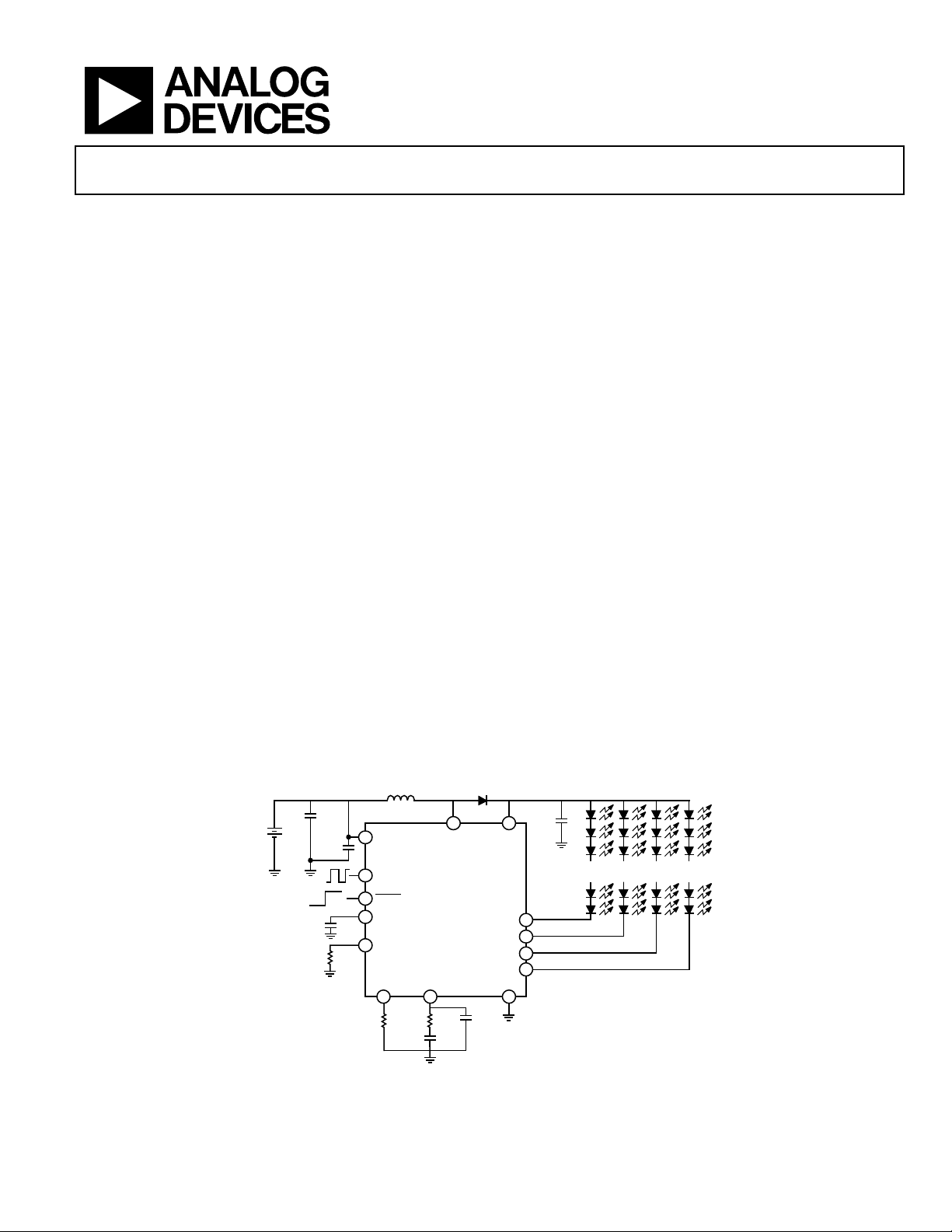
TYPICAL APPLICATION CIRCUIT
Figure 1.
One Technology Way, P.O. Box 9106, Norwood, MA 02062-9106, U.S.A.
Tel: 781.329.4700
www.analog.com

ADD5207 Data Sheet
TABLE OF CONTENTS
Features .............................................................................................. 1
Applications ....................................................................................... 1
General Description ......................................................................... 1
Typical Application Circuit ............................................................. 1
Revision History ............................................................................... 2
Functional Block Diagram .............................................................. 3
Specifications ..................................................................................... 4
Step-Up Switching Regulator Specifications ............................. 4
LED Current Regulation Specifications .................................... 5
General Specifications ................................................................. 6
Absolute Maximum Ratings ............................................................ 7
Thermal Resistance ...................................................................... 7
ESD Caution .................................................................................. 7
Pin Configuration and Function Descriptions ............................. 8
Typical Performance Characteristics ..............................................9
Theory of Operation ...................................................................... 11
Current Mode, Step-Up Switching Regulator Operation ..... 11
Internal 3.3 V Regulator ............................................................ 11
Boost Converter Switching Frequency .................................... 11
Dimming Frequency (f
Current Source ............................................................................ 11
PWM Dimming Mode .............................................................. 11
Safety Features ............................................................................ 11
External Component Selection Guide ..................................... 12
Layout Guidelines....................................................................... 13
Typical Application Circuits ......................................................... 15
Outline Dimensions ....................................................................... 16
Ordering Guide .......................................................................... 16
) ...................................................... 11
PWM
REVISION HISTORY
2/12—Rev. Sp0 to Rev. A
Replaced Block Diagram with Typical Application Circuit ........ 1
Changes to Features Section and General Description Section . 1
Changes to Current Mode, Step-Up Switching Regulator
Operation Section, Boost Converter Switching Frequency
Section, PWM Dimming Mode Section, Phase Shift PWM
Dimming Section, and Safety Features Section .......................... 11
Changes to Overvoltage Protection (OVP) Section .................. 11
Changes to Open-Loop Protection (OLP) Section,
Undervoltage Lockout (UVLO) Section, and Thermal
Protection Section .......................................................................... 12
Changes to Layout Guidelines Section ........................................ 13
7/09—Revision Sp0: Initial Version
Rev. A | Page 2 of 16

Data Sheet ADD5207
ADD5207
VIN VDD SHDN OVP
VOUT_FB
SW
LINEAR
REGULATOR
VOLTAGE
REFERENCE
SHUTDOWN
ERROR
AMP
UVP
COMP
PWM
COMP
UVP
REF
g
m
LL
REF
VOUT_FB
LL COMP
DCOMP
HEADROOM CO NTROL
CURRENT SOURCE 1
CURRENT SOURCE 2
CURRENT SOURCE 3
CURRENT SOURCE 4
PWM
500kΩ
ISET
REF
VDD
GND
500kΩ
GND
COMP
PWM
DUTY
EXTRACTOR
SOFT START
CURRENT SENSE
OSC
LED OPEN/SHORT
FAULT DETECTOR
DREF
OVP
REF
GND
THERMAL
SHUTDOWN
R
S
Q
FSLCT
GND
FB1
FB2
CURRENT SOURCE DRIVER
FPWM OSCILLATOR
1 108 13 14
2
12
4
5
FB3
6
FB4
7
9
3
11
08350-002
+
+
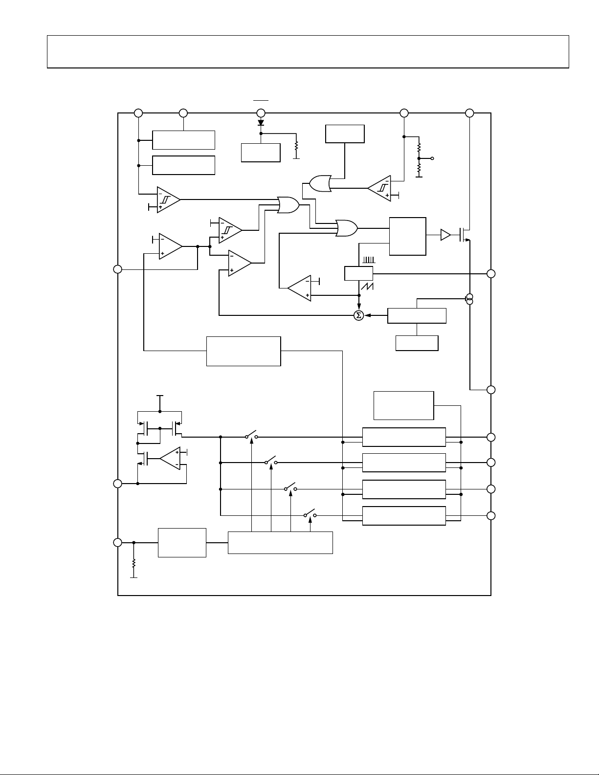
FUNCTIONAL BLOCK DIAGRAM
Figure 2. Functional Block Diagram
Rev. A | Page 3 of 16

ADD5207 Data Sheet
Parameter
Symbol
Test Conditions/Comments
Min
Typ
Max
Unit
SPECIFICATIONS
STEP-UP SWITCHING REGULATOR SPECIFICATIONS
VIN = 12 V,
Table 1.
SUPPLY
Input Voltage Range VIN 6 21 V
BOOST OUTPUT
Output Voltage V
SWITCH
On Resistance R
Leakage Current I
Peak Current Limit ICL Duty cycle (D) = D
OSCILLATOR
Switching Frequency fSW RF = 97 kΩ 800 1000 1200 kHz
Maximum Duty Cycle D
SOFT START
Soft Start Time tSS 1.1 ms
OVERVOLTAGE PROTECTION
Overvoltage Rising Threshold on OVP Pin V
Overvoltage Hysteresis on OVP Pin V
SHDN
= high, TA = −25°C to +85°C, unless otherwise noted. Typical values are at TA = +25°C.
36 V
OUT
DS(ON)
1 µA
LKG
RF = 97 kΩ 84 90 %
MAX
36.5 39 40 V
OVPR
OVP_HYS
VIN = 12 V, ISW = 100 mA 150 300 mΩ
MAX
0.1 0.7 1.4 V
1.5 A
Rev. A | Page 4 of 16

Data Sheet ADD5207
Current Matching Between Strings2
R
= 180 kΩ
−1.5 +1.5
%
LED CURRENT REGULATION SPECIFICATIONS
VIN = 12 V,
Table 2.
Parameter Symbol Test Conditions/Comments Min Typ Max Unit
CURRENT SOURCE
ISET Pin Voltage V
Adjustable LED Current1 I
Constant Current Sink of 20 mA2 I
Minimum Headroom Voltage2 V
LED Current Accuracy2 R
Current Source Leakage Current 1 µA
FPWM GENERATOR
Dimming Frequency f
LED FAULT DETECTION
Open Fault Delay1 t
1
This electrical specification is guaranteed by design.
2
Tested at TA = +25°C.
SHDN
= high, TA = −25°C to +85°C, unless otherwise noted. Typical values are at TA = +25°C.
6 V ≤ VIN ≤ 21 V 1.14 1.18 1.22 V
SET
0 25 mA
LED
R
LED20
R
HR20
PWM
D_OPENFAULT
6.5 µs
= 180 kΩ 19.4 20 20.6 mA
SET
= 180 kΩ 0.66 0.9 V
SET
SET
= 180 kΩ −3 +3 %
SET
6.8 8.0 9.2 kHz
Rev. A | Page 5 of 16
 Loading...