

Rail-to-Rail, Very Fast, 2.5 V to 5.5 V,
V
V
www.BDTIC.com/ADI
FEATURES
Fully specified rail to rail at V
Input common-mode voltage from −0.2 V to V
CML-compatible output stage
1.25 ns propagation delay
50 mW @ 2.5 V power supply
Shutdown pin
Single-pin control for programmable hysteresis and latch
(
ADCMP607 only)
Power supply rejection > 60 dB
−40°C to +125°C operation
APPLICATIONS
High speed instrumentation
Clock and data signal restoration
Logic level shifting or translation
Pulse spectroscopy
High speed line receivers
Threshold detection
Peak and zero-crossing detectors
High speed trigger circuitry
Pulse-width modulators
Current-/voltage-controlled oscillators
Automatic test equipment (ATE)
= 2.5 V to 5.5 V
CCI
+ 0.2 V
CCI
Single-Supply CML Comparators
ADCMP606/ADCMP607
GENERAL DESCRIPTION
The ADCMP606 and ADCMP607 are very fast comparators
fabricated on XFCB2, an Analog Devices, Inc., proprietary
process. These comparators are exceptionally versatile and easy
to use. Features include an input range from V
V
+ 0.2 V, low noise, CML-compatible output drivers, and
CCI
TTL-/CMOS-compatible latch inputs with adjustable hysteresis
and/or shutdown inputs.
The devices offer 1.25 ns propagation delay with 2.5 ps rms
ra
ndom jitter (RJ). Overdrive and slew rate dispersion are
typically less than 50 ps.
A flexible power supply scheme allows the devices to operate
th a single +2.5 V positive supply and a −0.5 V to +2.7 V
wi
input signal range up to a +5.5 V positive supply with a −0.5 V
to +5.7 V input signal range. The ADCMP607 features split
input/output supplies with no sequencing restrictions to
support a wide input signal range with independent output
swing control and power savings.
The CML-compatible output stage is fully back-matched for
erior performance. The comparator input stage offers robust
sup
protection against large input overdrive, and the outputs do not
phase reverse when the valid input signal range is exceeded. On
the ADCMP607, latch and programmable hysteresis features are
also provided with a unique single-pin control option.
The ADCMP606 is available in a 6-lead SC70 package and the
ADCMP607 is available in a 12-lead LFCSP package.
− 0.5 V to
EE
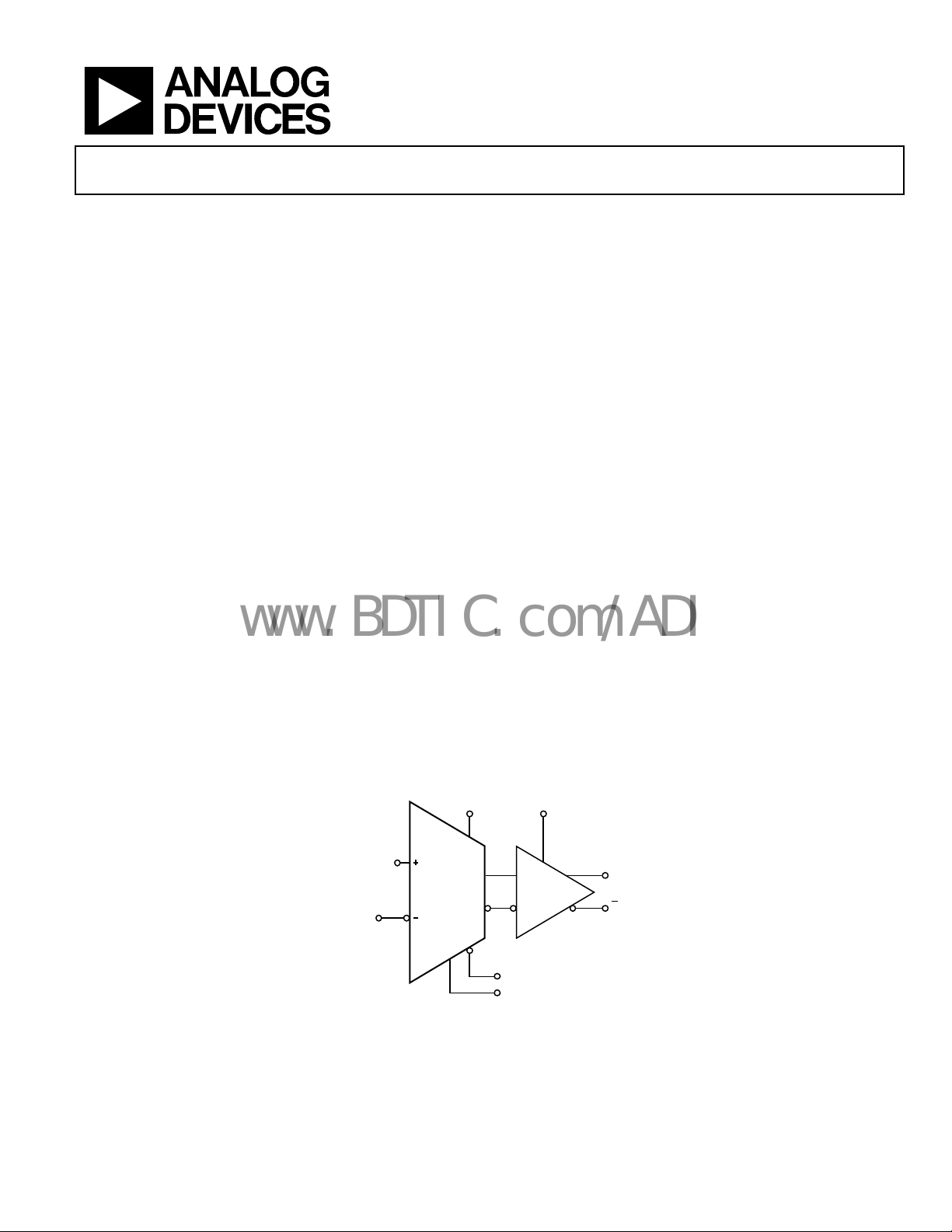
FUNCTIONAL BLOCK DIAGRAM
V
NONINVERTING
P
V
N
Rev. A
Information furnished by Analog Devices is believed to be accurate and reliable. However, no
responsibility is assumed by Anal og Devices for its use, nor for any infringements of patents or ot her
rights of third parties that may result from its use. Specifications subject to change without notice. No
license is granted by implication or otherwise under any patent or patent rights of Analog Devices.
Trademarks and registered trademarks are the property of their respective owners.
INVERTING
INPUT
INPUT
ADCMP606/
ADCMP607
CCO
(ADCMP607 ONLY )
CCI
CML
LE/HYS I NPUT (ADCMP 607 ONLY)
S
INPUT (ADCMP607 O NLY)
DN
Figure 1.
One Technology Way, P.O. Box 9106, Norwood, MA 02062-9106, U.S.A.
Tel: 781.329.4700 www.analog.com
Fax: 781.461.3113 ©2006–2007 Analog Devices, Inc. All rights reserved.
Q OUTPUT
Q OUTPUT
05917-001

ADCMP606/ADCMP607
www.BDTIC.com/ADI
TABLE OF CONTENTS
Features.............................................................................................. 1
Applications....................................................................................... 1
General Description ......................................................................... 1
Functional Block Diagram .............................................................. 1
Revision History ............................................................................... 2
Specifications..................................................................................... 3
Electrical Characteristics ............................................................. 3
Timing Information..................................................................... 5
Absolute Maximum Ratings............................................................ 6
Thermal Resistance ...................................................................... 6
ESD Caution.................................................................................. 6
Pin Configurations and Function Descriptions ........................... 7
Typical Performance Characteristics ............................................. 8
REVISION HISTORY
8/07—Rev. 0 to Rev. A
Changes to Specifications Section.................................................. 3
Changes to Table 3............................................................................ 6
Changes to Ordering Guide.......................................................... 14
10/06—Revision 0: Initial Version
Application Information................................................................ 10
Power/Ground Layout and Bypassing..................................... 10
CML-Compatible Output Stage ............................................... 10
Using/Disabling the Latch Feature........................................... 10
Optimizing Performance........................................................... 10
Comparator Propagation Delay Dispersion ........................... 11
Comparator Hysteresis .............................................................. 11
Crossover Bias Points................................................................. 12
Minimum Input Slew Rate Requirement................................ 12
Typical Application Circuits ......................................................... 13
Outline Dimensions....................................................................... 14
Ordering Guide .......................................................................... 14
Rev. A | Page 2 of 16
ADCMP606/ADCMP607
www.BDTIC.com/ADI
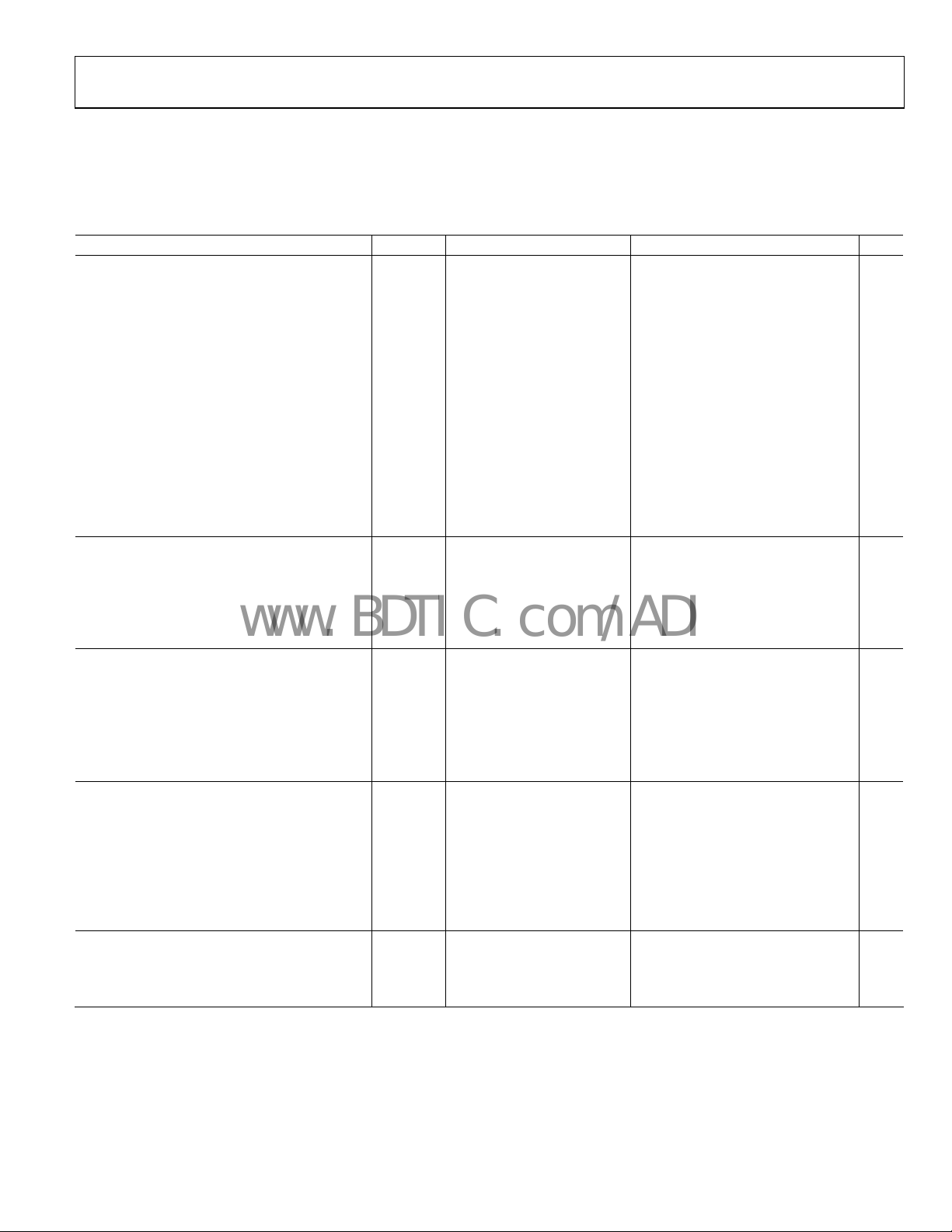
SPECIFICATIONS
ELECTRICAL CHARACTERISTICS
V
= V
CCI
Table 1.
Parameter Symbol Conditions Min Typ Max Unit
DC INPUT CHARACTERISTICS
Voltage Range VP, VN V
Common-Mode Range V
Differential Voltage V
Offset Voltage VOS −5.0 +5.0 mV
Bias Current IP, IN −5.0 ±2 +5.0 µA
Offset Current −2.0 2.0 µA
Capacitance CP, CN 1 pF
Resistance, Differential Mode −0.1 V to V
Resistance, Common Mode −0.5 V to V
Active Gain AV 85 dB
Hysteresis R
LATCH ENABLE PIN CHARACTERISTICS
(ADCMP607 Only)
VIH Hysteresis is shut off 2.0 V
VIL Latch mode guaranteed −0.2 +0.4 +0.8 V
IIH V
IIL V
HYSTERESIS MODE AND TIMING
Hysteresis Mode Bias Voltage Current sink 0 A 1.145 1.25 1.35 V
Minimum Resistor Value Hysteresis = 120 mV 55 75 110 kΩ
Latch Setup Time tS V
Latch Hold Time tH V
Latch-to-Output Delay t
Latch Minimum Pulse Width tPL V
SHUTDOWN PIN CHARACTERISTICS
(ADCMP607 Only)
VIH Comparator is operating 2.0 V
VIL Shutdown guaranteed −0.2 +0.4 +0.6 V
IIH V
IIL V
Sleep Time tSD 10% output swing <1 ns
Wake-Up Time tH V
DC OUTPUT CHARACTERISTICS V
Output Voltage High Level VOH 50 Ω terminate to V
Output Voltage Low Level VOL 50 Ω terminate to V
Output Voltage Differential 50 Ω terminate to V
= 2.5 V, TA = −40°C to +125°C, typical at TA = 25°C, unless otherwise noted.
CCO
= 2.5 V to 5.5 V −0.5 V
CCI
= 2.5 V to 5.5 V −0.2 V
CCI
= 2.5 V to 5.5 V V
CCI
200 700 kΩ
CCI
+ 0.5 V 100 350 kΩ
CCI
V
= 2.5 V, V
CCI
V
= −0.2 V to +2.7 V
CM
= 2..5 V, V
V
CCI
= ∞ <0.1 mV
HYS
= 2.5 V,
CCO
= 5.5 V 50 dB
CCO
= V
−6 +6 µA
IH
CCO
= 0.4 V −0.1 +0.1 mA
IL
= 50 mV −1.5 ns
OD
= 50 mV 2.3 ns
OD
, t
PLOH
VOD = 50 mV 30 ns
PLOL
= 50 mV 25 ns
OD
= V
−6 +6 µA
IH
CCO
= 0 V −0.1 mA
IL
= 100 mV, output valid 35 ns
OD
= 2.5 V to 5.5 V
CCO
+ 0.2 V
CCI
+ 0.2 V
CCI
V
CCI
50 dB Common-Mode Rejection Ratio CMRR
V
CCO
V
CCO
V
CCO
V
CCO
300 400 500 mV
CCO
− 0.1 V
CCO
− 0.6 V
CCO
− 0.05 V
CCO
− 0.45 V
CCO
V
CCO
− 0.3 V
CCO
Rev. A | Page 3 of 16
ADCMP606/ADCMP607
www.BDTIC.com/ADI
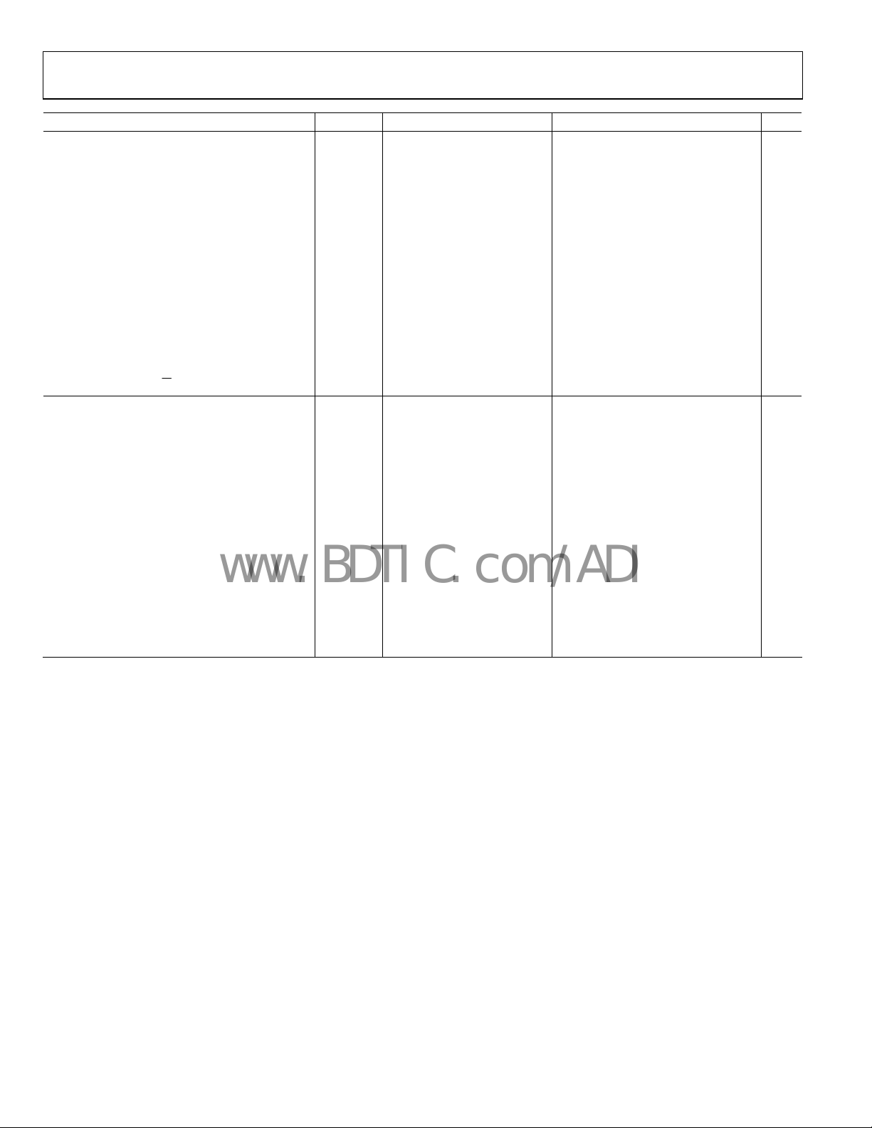
Parameter Symbol Conditions Min Typ Max Unit
AC PERFORMANCE
Rise Time/Fall time tR/tF
Propagation Delay tPD
Propagation Delay Skew—Rising to
Falling Transition
Overdrive Dispersion 10 mV < VOD < 125 mV 2.3 ns
Common-Mode Dispersion −0.2 V < VCM < VCC + 0.2 V 150 ps
Input Stage Bandwidth 750 MHz
RMS Random Jitter RJ VOD = 200 mV, 0.5 V/ns 2 ps
Minimum Pulse Width PW
Output Skew Q to Q
POWER SUPPLY
Input Supply Voltage Range V
Output Supply Voltage Range V
Positive Supply Differential (ADCMP607) V
V
Positive Supply Current (ADCMP606) I
V
Input Section Supply Current (ADCMP607) I
Output Section Supply Current (ADCMP607) I
I
Power Dissipation PD V
P
Power Supply Rejection Ratio PSRR V
Shutdown Mode I
Shutdown Mode I
1
VIN = 100 mV square input at 50 MHz, VCM = 2.5 V, V
1
10% to 90%,
= V
V
CCI
V
CCI
V
OD
V
CCI
V
OD
T
PINSKEW
MIN
VOD = 50 mV 40 ps
V
CCI
PW
T
DIFFSKEW
2.5 5.5 V
CCI
2.5 5.5 V
CCO
− V
CCI
− V
CCI
VCCI/V CCO
V
VCCI
V
VCCO
V
VCCO
V
D
V
CCI
V
CCO
= V
= 2.5 V, unless otherwise noted.
CCI
CCO
50%
Operating −3.0 +3.0 V
CCO
Nonoperating −6 +6 V
CCO
V
CCI
CCI
CCI
CCO
CCO
CCI
CCI
CCI
CCI
CCI
= 2.5 V to 5.5 V
CCO
= V
= 2.5 V to 5.5 V,
CCO
= 50 mV
= V
= 2.5 V,
CCO
= 10 mV
= V
= 5.5 V,
CCO
= 90% of PWIN
OUT
= V
= 2.5 V 11 17.5 21 mA
CCO
= V
= 5.5 V 16 20.5 26 mA
CCO
= 2.5 V 0.5 1.1 1.5 mA
= 2.5 V 10 15.8 18 mA
= 5.5 V 16 18 25 mA
= V
= 2.5 V 30 46 55 mW
CCO
= V
= 5.5 V 90 110 150 mW
CCO
= 2.5 V to 5 V −50 dB
= V
= 2.5 V to 5 V 200 240 800 µA
CCO
= V
= 2.5 V to 5 V −30 30 µA
CCO
160 ps
1.2 ns
2.1 ns
1.1 ns
20 ps
Rev. A | Page 4 of 16
ADCMP606/ADCMP607
www.BDTIC.com/ADI
TIMING INFORMATION
Figure 2 illustrates the ADCMP606/ADCMP607 latch timing relationships. Tabl e 2 provides definitions of the terms shown in Figure 2.
1.1V
LATCH ENABLE
DIFFERENTIAL
INPUT VOLTAGE
Q OUTPUT
Q OUTPUT
t
S
t
H
V
IN
V
OD
t
PDL
t
PDH
Figure 2. System Timing Diagram
t
t
R
t
PL
t
PLOH
F
t
PLOL
Table 2. Timing Descriptions
Symbol Timing Description
tF Output fall time
tH Minimum hold time
Amount of time required to transition from a high to a low output as measured at the 20%
and 80% poin
ts.
Minimum time after the negative transition of the la
must remain unchanged to be acquired and held at the outputs.
t
Input to output high delay
PDH
Propagation delay measured from the time the i
input offset voltage) to the 50% point of an output low-to-high transition.
t
Input to output low delay
PDL
Propagation delay measured from the time the i
input offset voltage) to the 50% point of an output high-to-low transition.
tPL Minimum latch enable pulse width
t
Latch enable to output high delay
PLOH
t
Latch enable to output low delay
PLOL
tR Output rise time
Minimum time that the latch enable signal must be high to acquire an input signal
.
change
Propagation delay measured from the 50% point of the latch enable signal low-to-high
transition to the
50% point of an output low-to-high transition.
Propagation delay measured from the 50% point of the latch enable signal low-to-high
ansition to the 50% point of an output high-to-low transition.
tr
Amount of time required to transition from a
low to a high output as measured at the 20%
and 80% points.
tS Minimum setup time
Minimum time before the negative transition of
input signal change must be present to be acquired and held at the outputs.
VOD Voltage overdrive Difference between the input voltages VA and VB.
V
± V
N
OS
50%
50%
05917-025
tch enable signal that the input signal
nput signal crosses the reference (± the
nput signal crosses the reference (± the
the latch enable signal occurs that an
Rev. A | Page 5 of 16
ADCMP606/ADCMP607
www.BDTIC.com/ADI
ABSOLUTE MAXIMUM RATINGS
Table 3.
Parameter Rating
Supply Voltages
Input Supply Voltage (V
Output Supply Voltage
to GND)
(V
CCO
Positive Supply Differential
− V
CCO
)
(V
CCI
Input Voltages
Input Voltage −0.5 V to V
Differential Input Voltage ±( V
Maximum Input/Output Current ±50 mA
Shutdown Control Pin
Applied Voltage (SDN to GND) −0.5 V to V
Maximum Input/Output Current ±50 mA
Latch/Hysteresis Control Pin
Applied Voltage (HYS to GND) −0.5 V to V
Maximum Input/Output Current ±50 mA
Output Current ±50 mA
Temperature
Operating Temperature, Ambient −40°C to +125°C
Operating Temperature, Junction 150°C
Storage Temperature Range −65°C to +150°C
to GND) −0.5 V to +6.0 V
CCI
−0.5 V to +6.0 V
−6.0 V to +6.0 V
+ 0.5 V
CCI
+ 0.5 V)
CCI
+ 0.5 V
CCO
+ 0.5 V
CCO
Stresses above those listed under Absolute Maximum Ratings
may cause permanent damage to the device. This is a stress
rating only; functional operation of the device at these or any
other conditions above those indicated in the operational
section of this specification is not implied. Exposure to absolute
maximum rating conditions for extended periods may affect
device reliability.
THERMAL RESISTANCE
θJA is specified for the worst-case conditions, that is, a device
soldered in a circuit board for surface-mount packages.
Table 4. Thermal Resistance
Package Type θ
ADCMP606 6-Lead SC70 426 °C/W
ADCMP607 12-Lead LFCSP 62 °C/W
1
Measurement in still air.
1
Unit
JA
ESD CAUTION
Rev. A | Page 6 of 16

ADCMP606/ADCMP607
www.BDTIC.com/ADI
PIN CONFIGURATIONS AND FUNCTION DESCRIPTIONS
12 Q
11 VEE10 Q
1
Q
ADCMP606
2
V
EE
V
P
TOP VIEW
(Not to Scale)
3
Figure 3. ADCMP606 Pin Configuration Figure 4. ADCMP607 Pin Configuration
Table 5. ADCMP606 (6-Lead SC70) Pin Function Descriptions
Pin No. Mnemonic Description
1 Q
2 VEE Negative Supply Voltage.
3 V
4 V
5 V
6
Noninverting Analog Input.
P
Inverting Analog Input.
N
Input Section Supply/Output Section Supply. Shared pin.
CCI/VCCO
Q Inverting Output. Q is at logic low if the analog voltage at the noninverting input, VP, is greater than the
6
Q
5
V
CCI/VCCO
4
V
N
05917-002
Noninverting Output. Q is at logic high if the analog
the analog voltage at the inverting input, V
.
N
analog voltage at the inverting input, VIN.
PIN 1
1
2
3
INDICATOR
ADCMP607
TOP VIEW
(Not to Scal e)
4
5
P
V
V
V
CCO
V
CCI
V
EE
9 V
EE
8 LE/HYS
7 S
DN
6
N
EE
V
voltage at the noninverting input, V
05917-003
, is greater than
P
Table 6. ADCMP607 (12-Lead LFCSP) Pin F
unction Descriptions
Pin No. Mnemonic Description
1 V
2 V
3 V
4 V
5 V
6 V
7 S
8 LE/HYS
9 V
10
Output Section Supply.
CCO
Input Section Supply.
CCI
Negative Supply Voltage.
EE
Noninverting Analog Input.
P
Negative Supply Voltage.
EE
Inverting Analog Input.
N
Shutdown. Drive this pin low to shut down the device.
DN
Latch/Hysteresis Control. Bias with resistor or current for hysteresis adjustment; drive low to latch.
Negative Supply Voltage.
EE
Q Inverting Output. Q is at logic low if the analog voltage at the noninverting input, VP, is greater than the
analog voltage at the inverting input, VN, if the comparator is in compare mode.
11 VEE Negative Supply Voltage.
12 Q
Noninverting Output. Q is at logic high if the analog voltage at the noninverting input, V
the analog voltage at the inverting input, V
V
Heat Sink
P
addle
EE
The metallic back surface of the package is electrically connected to VEE. It can be left floating because
in 3, Pin 5, Pin 9, and Pin 11 provide adequate electrical connection. It can also be soldered to the
P
application board if improved thermal and/or mechanical stability is desired.
, if the comparator is in compare mode.
N
, is greater than
P
Rev. A | Page 7 of 16

ADCMP606/ADCMP607
www.BDTIC.com/ADI
TYPICAL PERFORMANCE CHARACTERISTICS
V
= V
CCI
= 2.5 V, TA = 25°C, unless otherwise noted.
CCO
800
600
400
200
0
–200
CURRENT (µA)
–400
–600
–800
–101 23 456 7
LE/HYS PIN (V)
VCC = 5.5VVCC = 2.5V
Figure 5. LE/HYS Pin Current vs. Voltage
250
200
150
100
HYSTERESIS (mV)
50
0
05917-026
0 –2 –4 –6 –8 –10 –12 –14 –16 –18
+25°C
+125°C
LE/HYS PI N CURRENT (µA)
–40°C
05917-004
Figure 8. Hysteresis vs. LE/HYS Pin Current
200
150
100
VCC = 5.5VVCC = 2.5V
50
0
CURRENT (µA)
–50
–100
–150
–1 0 1 2 3 4 5 6 7
Figure 6. S
10
8
6
4
2
0
(µA)
B
I
–2
–4
–6
–8
–10
–1.0 –0.5 0 0.5 1.0 1.5 2.0 2.5 3. 0 3.5
–40°C
+25°C
+125°C
SDN PIN (V)
Pin Current vs. Voltage
DN
VCM AT VCC = 2.5V
Figure 7. Input Bias Current vs. Input Common-Mode Voltage
400
350
300
250
200
150
HYSTERESIS (mV)
100
50
0
05917-007
50 100 150 200 250 300 35 0 400 450 500 550 600 650
Figure 9. Hysteresis vs. Hysteresis R
3.5
3.0
2.5
2.0
PROPAGATI ON DELAY (n s)
1.5
PROPAGATI ON DELAY RISE
1.0
05917-006
0 10 20 30 40 50 60 70 80 90 100 110 120 130 140
VCC = 2.5V
HYS RESISTOR (kΩ)
PROPAGATION DELAY FALL
OVERDRIVE (mV)
esistor
05917-005
05917-009
Figure 10. Propagation Delay vs. Input Overdrive
Rev. A | Page 8 of 16

ADCMP606/ADCMP607
www.BDTIC.com/ADI
1.4
PROPAGATI ON DELAY F ALL ns
1.3
1.2
PROPAGATI ON DELAY (n s)
PROPAGATI ON DELAY RI SE ns
5.550V
Q
1.1
–0.2 0.2 0.6 1.0 1.4 1.8 2.2 2.6 3.0
VCM AT VCC = 2.5V
Figure 11. Propagation Delay vs. Input Common-Mode Voltage
2.550V
2.050V 1.000ns/DI V
Figure 12 .Output Waveform at V
Q
Q
= 2.5 V
CC
Q
5.050V 1. 000ns/DIV
05917-010
Figure 13. Output Waveform at V
= 5.5 V
CC
5917-012
05917-011
Rev. A | Page 9 of 16

ADCMP606/ADCMP607
V
www.BDTIC.com/ADI
APPLICATION INFORMATION
POWER/GROUND LAYOUT AND BYPASSING
The ADCMP606/ADCMP607 comparators are very high speed
devices. Despite the low noise output stage, it is essential to use
proper high speed design techniques to achieve the specified
performance. Because comparators are uncompensated amplifiers,
feedback in any phase relationship is likely to cause oscillations
or undesired hysteresis. Of critical importance is the use of low
impedance supply planes, particularly the output supply plane
(V
) and the ground plane (GND). Individual supply planes
CCO
are recommended as part of a multilayer board. Providing the
lowest inductance return path for switching currents ensures
the best possible performance in the target application.
It is also important to adequately bypass the input and output
upplies. Multiple high quality 0.01 μF bypass capacitors should
s
be placed as close as possible to each of the V
CCI
and V
CCO
supply
pins and should be connected to the GND plane with redundant
vias. At least one of these should be placed to provide a physically
short return path for output currents flowing back from ground
to the V
CCI
and V
pins. High frequency bypass capacitors
CCO
should be carefully selected for minimum inductance and ESR.
Parasitic layout inductance should also be strictly controlled to
maximize the effectiveness of the bypass at high frequencies.
CML-COMPATIBLE OUTPUT STAGE
Specified propagation delay dispersion performance can be
achieved by using proper transmission line terminations. The
outputs of the ADCMP606 and ADCMP607 are designed to drive
400 mV directly into a 50 Ω cable or into transmission lines
terminated using either microstrip or strip line techniques with
50 Ω referenced to V
simplified schematic diagram in Figure 14. Each output is backt
erminated with 50 Ω for best transmission line matching.
Figure 14. Simplified Schematic Diagram of
. The CML output stage is shown in the
CCO
CCO
50Ω
Q
Q
16mA
CML-Comp
GND
atible Output Stage
05917-013
If these high speed signals must be routed more than a centimeter,
then either microstrip or strip line techniques are required to
ensure proper transition times and to prevent excessive output
ringing and pulse width dependent propagation delay
dispersion.
It is also possible to operate the outputs with the internal
t
ermination only if greater output swing is desired. This can be
especially useful for driving inputs on CMOS devices intended
for full swing ECL and PECL, or for generating pseudo PECL
levels. To avoid deep saturation of the outputs and resulting
pulse dispersion, V
must be kept above the specified
CCO
minimum output low level (see the Electrical Characteristics
ection). The line length driven should be kept as short as
s
possible.
USING/DISABLING THE LATCH FEATURE
The latch input is designed for maximum versatility. It can
safely be left floating or it can be driven low by any standard
TTL/CMOS device as a high speed latch.
In addition, the pin can be operated as a hysteresis control pin
th a bias voltage of 1.25 V nominal and an input resistance of
wi
approximately 70 kΩ. This allows the comparator hysteresis to
be easily controlled by either a resistor or an inexpensive CMOS
DAC. Driving this pin high or floating the pin removes all
hysteresis.
Hysteresis control and latch mode can be used together if an
o
pen-drain, an open-collector, or a three-state driver is con-
nected parallel to the hysteresis control resistor or current source.
Due to the programmable hysteresis feature, the logic threshold
the latch pin is approximately 1.1 V regardless of V
of
CCO
.
OPTIMIZING PERFORMANCE
As with any high speed comparator, proper design and layout
techniques are essential for obtaining the specified performance.
Stray capacitance, inductance, inductive power and ground
impedances, or other layout issues can severely limit performance
and often cause oscillation. Large discontinuities along input
and output transmission lines can also limit the specified pulse
width dispersion performance. The source impedance should
be minimized as much as is practicable. High source impedance,
in combination with the parasitic input capacitance of the
comparator, causes an undesirable degradation in bandwidth at
the input, thus degrading the overall response. Thermal noise
from large resistances can easily cause extra jitter with slowly
slewing input signals; higher impedances encourage undesired
coupling.
Rev. A | Page 10 of 16

ADCMP606/ADCMP607
www.BDTIC.com/ADI
COMPARATOR PROPAGATION DELAY DISPERSION
The ADCMP606/ADCMP607 comparators are designed to
reduce propagation delay dispersion over a wide input overdrive
range of 5 mV to V
variation in propagation delay that results from a change in the
degree of overdrive or slew rate (that is, how far or how fast the
input signal exceeds the switching threshold).
Propagation delay dispersion is a specification that becomes
i
mportant in high speed, time-critical applications, such as data
communication, automatic test and measurement, and instrumentation. It is also important in event-driven applications, such
as pulse spectroscopy, nuclear instrumentation, and medical
imaging. Dispersion is defined as the variation in propagation
delay as the input overdrive conditions are changed (
a
nd Figure 16).
The device dispersion is typically 2.3 ns as the overdrive varies
f
rom 10 mV to 125 mV. This specification applies to both
positive and negative signals because each device has very closely
matched delays for positive-going and negative-going inputs as
well as very low output skews.
INPUT VOLTAG E
Q/Q OUTPUT
Figure 15. Propagation Delay—Overdrive Dispersion
INPUT VOLTAGE
− 1 V. Propagation delay dispersion is the
CCI
Figure 15
500mV OVERDRIVE
10mV OVERDRIVE
V
± V
N
OS
DISPERSION
05917-014
1V/ns
± V
V
N
10V/ns
OS
switching threshold becomes −V
the high state until the new threshold, −V
below the threshold region in a negative direction. In this manner,
noise or feedback output signals centered on 0 V input cannot
cause the comparator to switch states unless it exceeds the region
bounded by ±V
/2.
H
OUTPUT
–V
H
2
Figure 17. Comparator Hysteresis Transfer Function
The customary technique for introducing hysteresis into a
comparator uses positive feedback from the output back to
the input. One limitation of this approach is that the amount
of hysteresis varies with the output logic levels, resulting in
hysteresis that is not symmetric about the threshold. The
external feedback network can also introduce significant
parasitics that reduce high speed performance and induce
oscillation in some cases.
This ADCMP607 comparator offers a programmable hysteresis
ature that can significantly improve accuracy and stability.
fe
Connecting an external pull-down resistor or a current source
from the LE/HYS pin to GND, varies the amount of hysteresis
in a predictable, stable manner. Leaving the LE/HYS pin disconnected or driving this pin high removes hysteresis. The maximum
hysteresis that can be applied using this pin is approximately
160 mV.
fun
typ
Figure 18 illustrates typical hysteresis applied as a
ction of the external resistor value, and Figure 7 illustrates
ical hysteresis as a function of the current.
400
/2. The comparator remains in
H
/2, is crossed from
H
V
OH
V
OL
0
INPUT
+V
H
2
05917-016
DISPERSIO N
Q/Q OUTPUT
Figure 16. Propagation Delay—Slew Rate Dispersion
05917-015
COMPARATOR HYSTERESIS
The addition of hysteresis to a comparator is often desirable in
a noisy environment, or when the differential input amplitudes
are relatively small or slow moving. Figure 17 shows the transfer
f
unction for a comparator with hysteresis. As the input voltage
approaches the threshold (0 V, in this example) from below the
threshold region in a positive direction, the comparator switches
from low to high when the input crosses +V
/2, and the new
H
Rev. A | Page 11 of 16
350
300
250
200
150
HYSTERESIS (mV)
100
50
0
50 100 150 200 250 300 35 0 400 450 500 550 600 650
Figure 18. Hysteresis vs. R
VCC = 2.5V
HYS RESISTOR (kΩ)
Control Resistor
HYS
05917-017

ADCMP606/ADCMP607
www.BDTIC.com/ADI
The hysteresis control pin appears as a 1.25 V bias voltage seen
through a series resistance of 70 kΩ ± 20% throughout the
hysteresis control range. The advantages of applying hysteresis in
this manner are improved accuracy, improved stability, reduced
component count, and maximum versatility. An external bypass
capacitor is not recommended on the LE/HYS pin because it
impairs the latch function and often degrades the jitter performance of the device. As described in the
tch Feature section, hysteresis control need not compromise
La
th
e latch function.
Using/Disabling the
CROSSOVER BIAS POINTS
In both op amps and comparators, rail-to-rail inputs of this type
have a dual front-end design. Certain devices are active near the
V
rail and others are active near the VEE rail. At some predeter-
CCI
mined point in the common-mode range, a crossover occurs. At
this point, normally VCCI/2, the direction of the bias current
reverses and the measured offset voltages and currents change.
The ADCMP606/ADCMP607 comparators slightly elaborate
o
n this scheme. Crossover points are found at approximately
0.6 V and 1.6 V common mode.
MINIMUM INPUT SLEW RATE REQUIREMENT
With the rated load capacitance and normal good PCB design
practice, as discussed in the Optimizing Performance section,
hese comparators should be stable at any input slew rate with
t
no hysteresis. Broadband noise from the input stage is observed
in place of the violent chattering seen with most other high
speed comparators. With additional capacitive loading or poor
bypassing, oscillation is observed. This oscillation is due to the
high gain bandwidth of the comparator in combination with
feedback parasitics in the package and PC board. In many
applications, chattering is not harmful.
Rev. A | Page 12 of 16
ADCMP606/ADCMP607
V
V
V
C
V
±
V
V
V
V
V
www.BDTIC.com/ADI
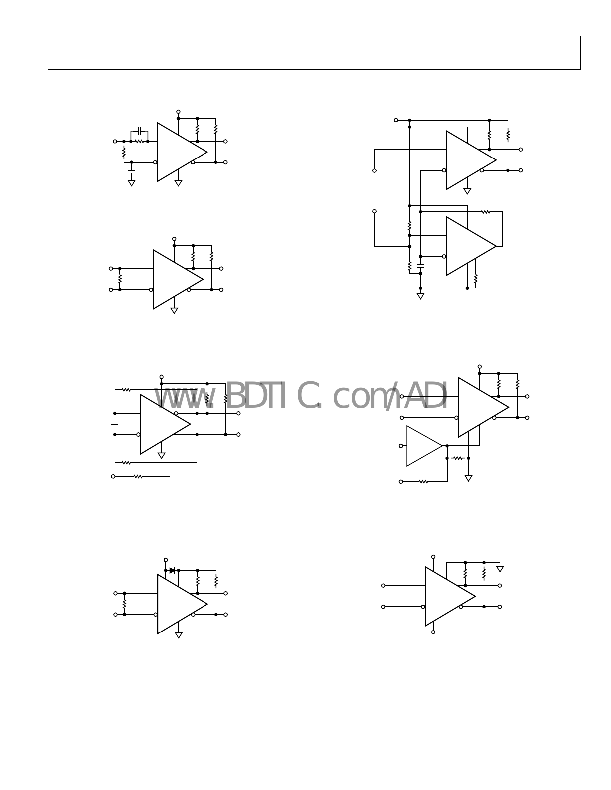
TYPICAL APPLICATION CIRCUITS
2.5V TO 5
5
ADCMP606
2.5V
2.5V
REF
10kΩ
10kΩ
ADCMP601
10kΩ
150pF
LE/HYS
100kΩ
Figure 23. Oscillator and Pulse-Width Modulator
50Ω 50Ω
CML
PWM
OUTPUT
05917-022
INPUT
LVDS
0.1µF
2kΩ
2kΩ
ADCMP606
0.1µF
Figure 19. Self-Biased, 50% Slicer
3.3
100Ω
ADCMP606
Figure 20. LVDS to CML
50Ω 50Ω
50Ω 50Ω
CML
OUTPUT
CML
OUTPUT
INPUT
05917-018
05917-019
50m
INPUT
5
10kΩ
82pF
ADCMP607
LE/HYS
ONTROL
CURRENT
10kΩ
10kΩ
Figure 21. Current-Controlled Oscillator
3.3
1N4001
V
CCO
50Ω 50Ω
LVDS
100Ω
V
CCI
ADCMP607
Figure 22. Fake PECL Levels Using a Series Diode
50Ω 50Ω
3.3V
PECL
CML
OUTPUT
05917-021
2.5V TO 5
50Ω 50Ω
ADCMP607
DIGITAL
CONTROL
05917-020
VOLTAGE
0V TO 2. 5
INPUT
74 VHC
1G07
150kΩ
150kΩ
LE/HYS
05917-023
Figure 24. Hysteresis Adjustment with Latch
+2.5V – 3
V
CCI
ADCMP607
–2.5V
V
EE
V
CCO
50Ω 50Ω
OUTPUT
05917-024
Figure 25. Ground-Referenced CML with ±3 V Input Range
Rev. A | Page 13 of 16

ADCMP606/ADCMP607
www.BDTIC.com/ADI
OUTLINE DIMENSIONS
2.20
2.00
1.80
2.40
1.35
1.25
1.15
PIN 1
1.30 BSC
1.00
0.90
0.70
0.10 MAX
0.10 COPLANARITY
COMPLIANT TO JEDEC STANDARDS MO-203-AB
Figure 26. 6-Lead Thin Shrink Small Outline Transistor Package [SC70]
3.00
BSC SQ
PIN 1
INDICATOR
1.00
0.85
0.80
SEATING
PLANE
12° MAX
TOP
VIEW
0.80 MAX
0.65 TYP
0.30
0.23
0.18
*
COMPLIANT TO JEDEC STANDARDS MO-220-VEED-1
EXCEPT FO R EXPOSED PAD DI MENSION.
Figure 27. 12-Lead Lead Frame Chip Scale Package [LFCSP_VQ]
4 5 6
2.10
3 2 1
1.80
0.65 BSC
0.40
0.10
0.30
0.15
1.10
0.80
SEATING
PLANE
(K
S-6)
Dimensions shown in millimeters
0.60 MAX
0.45
2.75
BSC SQ
EXPOSED PAD
(BOTTOM VIEW )
0.05 MAX
0.02 NOM
0.20 REF
3
mm × 3 mm Body, Very Thin Quad
9
8
7
0.50
BSC
COPLANARITY
0.08
(CP-12-1)
Dimensions shown in millimeters
0.22
0.08
10
0.46
0.36
0.26
0.75
0.55
0.35
11
12
1
2
3
6
5
4
PIN 1
INDICATOR
*
1.45
1.30 SQ
1.15
0.25 MIN
ORDERING GUIDE
Model Temperature Range Package Description
ADCMP606BKSZ-R2
ADCMP606BKSZ-RL
ADCMP606BKSZ-REEL71−40°C to +125°C 6-Lead Thin Shrink Small Outline Transistor Package [SC70] KS-6 G0S
ADCMP607BCPZ-R2
ADCMP607BCPZ-R7
ADCMP607BCPZ-WP
1
Z = RoHS Compliant Part.
1
1
−40°C to +125°C 6-Lead Thin Shrink Small Outline Transistor Package [SC70] KS-6 G0S
−40°C to +125°C 6-Lead Thin Shrink Small Outline Transistor Package [SC70] KS-6 G0S
1
−40°C to +125°C 12-Lead Lead Frame Chip Scale Package [LFCSP_VQ] CP-12-1 G0H
1
−40°C to +125°C 12-Lead Lead Frame Chip Scale Package [LFCSP_VQ] CP-12-1 G0H
1
−40°C to +125°C 12-Lead Lead Frame Chip Scale Package [LFCSP_VQ] CP-12-1 G0H
Rev. A | Page 14 of 16
Package
Op
tion Branding

ADCMP606/ADCMP607
www.BDTIC.com/ADI
NOTES
Rev. A | Page 15 of 16

ADCMP606/ADCMP607
www.BDTIC.com/ADI
NOTES
©2006–2007 Analog Devices, Inc. All rights reserved. Trademarks and
registered trademarks are the property of their respective owners.
D05917-0-8/07(A)
Rev. A | Page 16 of 16
 Loading...